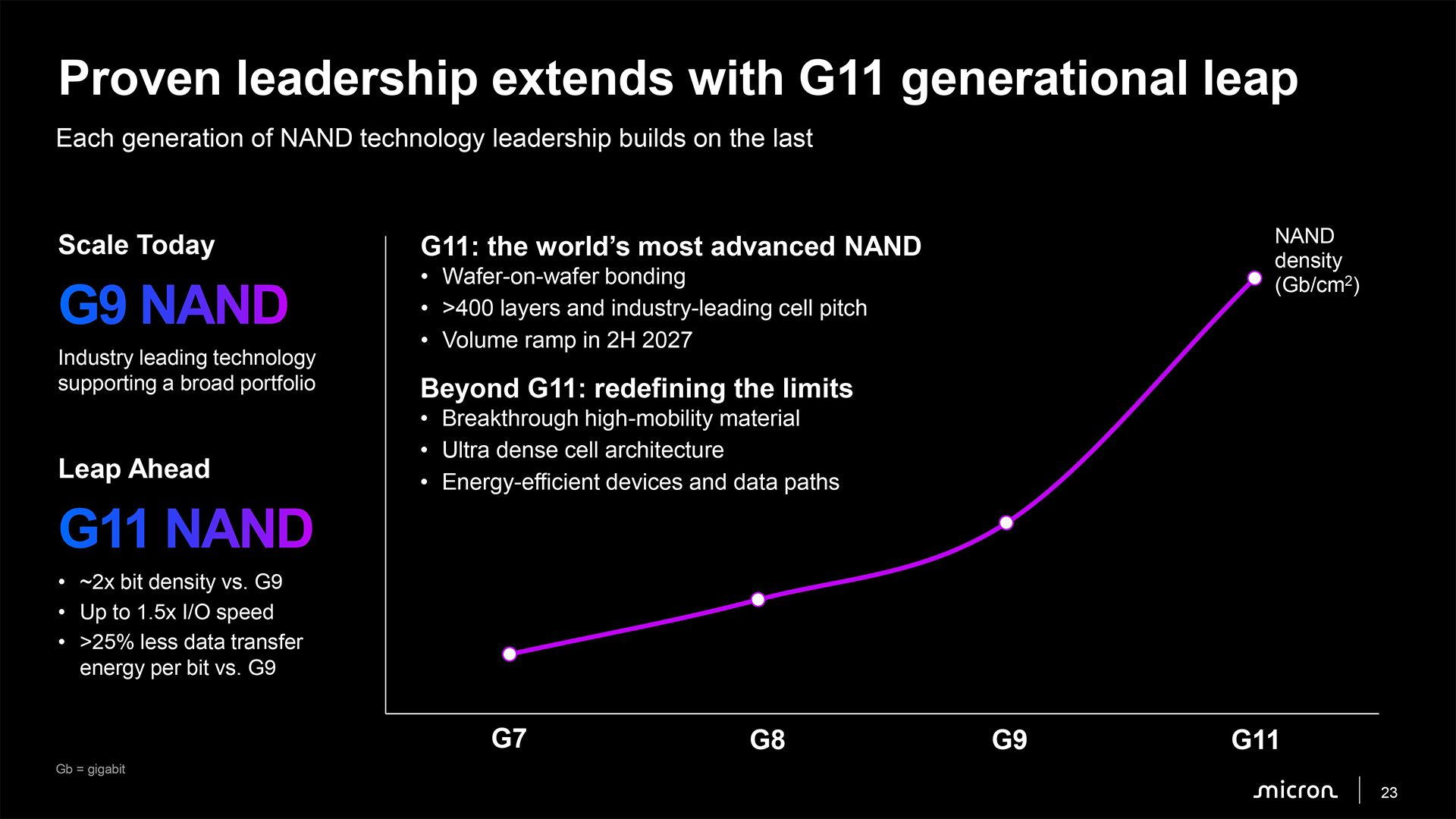
Micron's next-generation 3D NAND, which will enter mass production in 2H 2027, is set to offer three significant advantages: it will double storage density, increase I/O performance by 50% compared to the company's current-generation NAND memory, and decrease power consumption, the company revealed at an event this week. To achieve these aggressive goals, Micron plans to take a page from YMTC's book and adopt wafer-on-wafer bonding. Meanwhile, Micron is also developing new materials and denser memory cell architectures to extend 3D NAND scaling beyond G11.
"We had mentioned we will bring in wafer-on-wafer bonding technology at the right time when it’s cost-effective, and it brings in capability that is important for the product specs at the time, and this is the right timing for that technology," said Scott DeBoer, president and chief technology and products officer at Micron, during the company's event this week. "So this G11 technology is the world's most advanced NAND. It will ramp in the second half of next year, [and] it is based on wafer-on-wafer bonding technology."
G11: Over 400 layers and wafer bonding
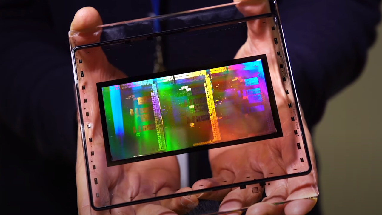
Micron's G11 3D NAND represents a substantial advancement over its current G9 (N160) generation. The company expects the new memory to achieve approximately twice the bit density of G9 (3D TLC 21 Gb/mm2 => 3D TLC 42 Gb/mm2?), which means a dramatic increase compared to Kioxia's BiCS10 or Samsung's V10; increase I/O speeds by up to 50% (3,600 MT/s => 5,400 MT/s?); and reduce data transfer energy consumption per bit by more than 25%.
These improvements should benefit both conventional high-capacity SSDs for client and data center applications and emerging AI-oriented storage devices, which require greater bandwidth and energy efficiency.
(Image credit: Micron)
One of the key changes introduced with G11 is wafer-on-wafer bonding, which enables Micron to manufacture different parts of its NAND device on separate wafers using different process technologies — a new 3D NAND node to build a NAND array and a logic fabrication process to make peripheral circuits and I/O — and subsequently bond them together. The company has used CMOS-under-array architectures for several generations. Still, wafer bonding provides additional flexibility to optimize memory arrays and peripheral logic independently, which means more capacity and performance if all goes as planned.
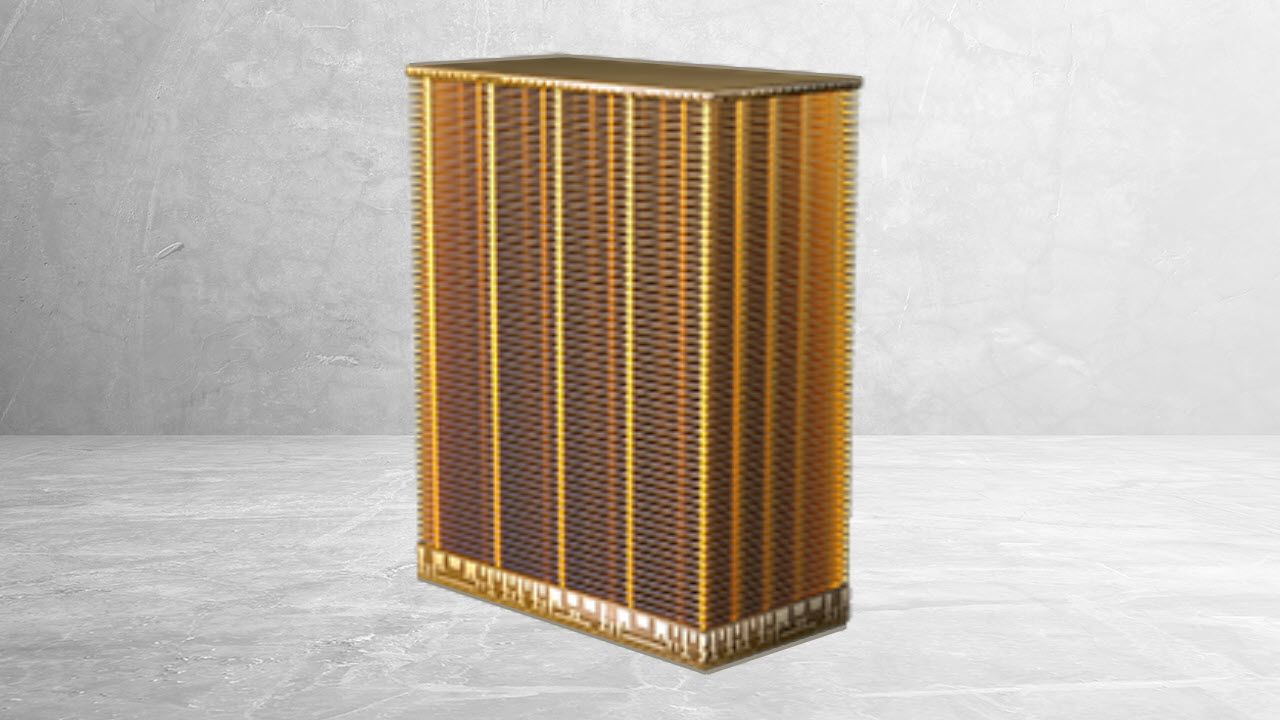
Another important innovation is the transition to more than 400 NAND layers. Micron has not disclosed the exact number of active wordline layers or the number of memory decks used by G11, but the company says the technology will feature an industry-leading memory cell pitch, which suggests that its density improvements will come from both additional layers and smaller cell dimensions.
Micron expects to disclose more technical details about G11 in 2027, closer to the start of high-volume manufacturing in the second half of next year.
Beyond G11: New materials and denser memory cells
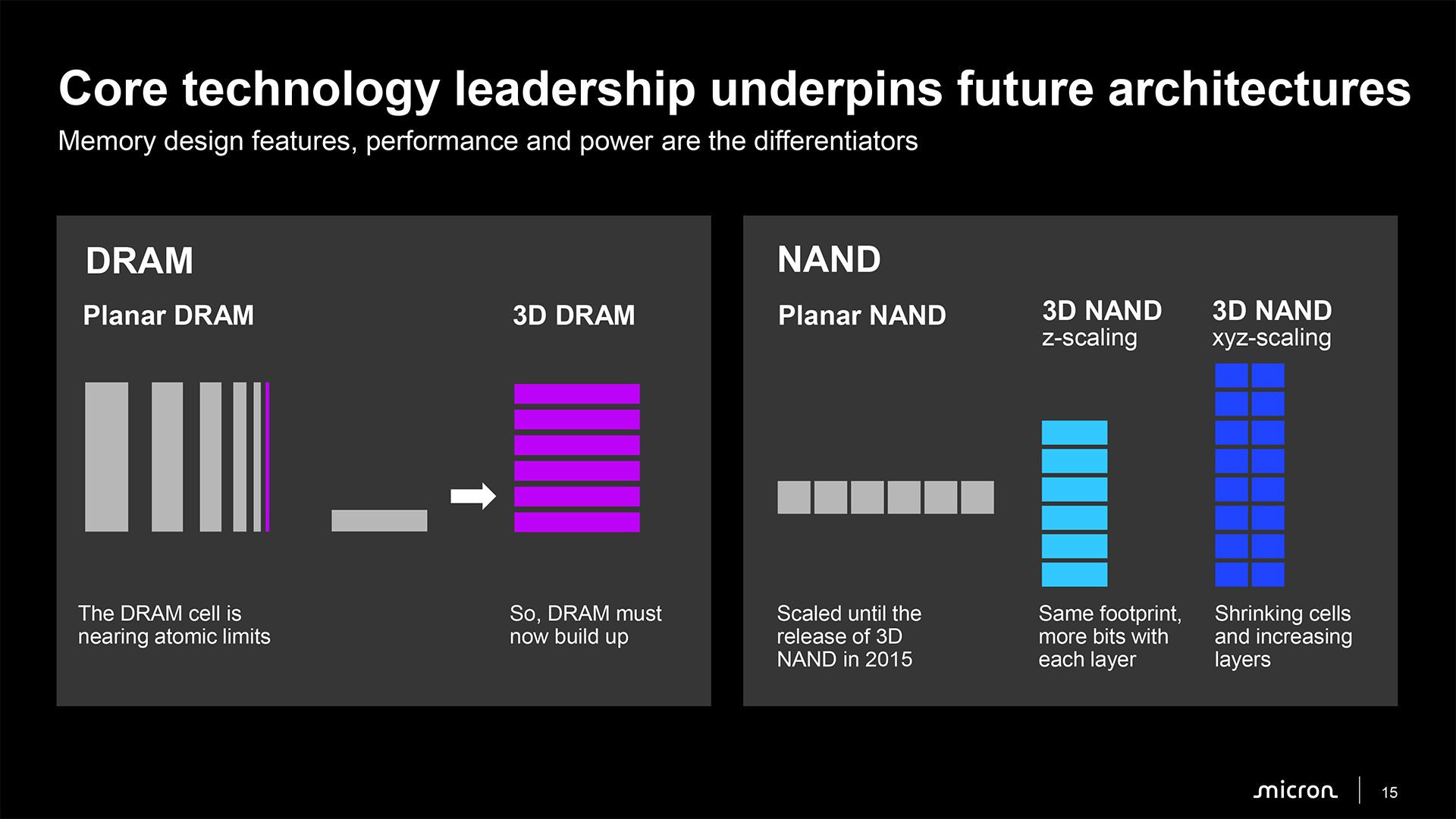
Without any doubt, Micron will continue scaling 3D NAND along all three dimensions rather than simply increasing the number of layers going forward. While conventional 3D NAND scaling initially relied primarily on adding more memory layers, future generations will also require reductions in cell dimensions along the X and Y axes to improve bit density while keeping manufacturing complexity in check.
(Image credit: Micron)
To achieve this, Micron is developing what it describes as breakthrough high-mobility materials, ultra-dense cell architectures, and more energy-efficient devices and data paths. These technologies could improve transistor characteristics, enable further reductions in memory cell dimensions, and reduce the energy required to move data within NAND devices.
"Beyond G11, we have a strong roadmap, not going to go into great detail on it today, but really focused on new materials densifying the cell architecture, and continuing to focus on that XYZ scaling going forward," said DeBoer. "[…] The current industry direction and Micron’s direction is scaling both by adding layers [and] also by shrinking the cell dimensions."
The company has not disclosed specific architectural details, density targets, or production schedules for its post-G11 generations, though its roadmap suggests that future NAND scaling will increasingly depend on innovations in materials, cell architecture, and peripheral circuitry rather than layer-count increases alone. Meanwhile, since the number of active layers is arguably the easiest way to increase storage density, we would not expect the race towards the highest layer count to slow down substantially in the coming years, especially given strong demand for 3D NAND-based storage.
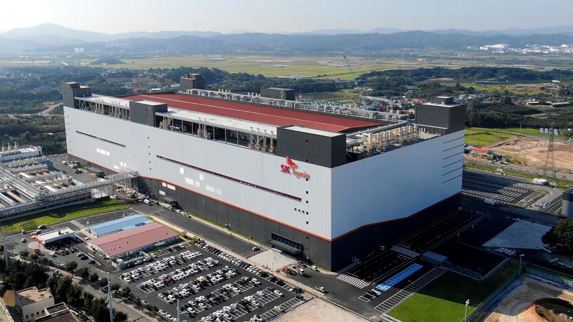
SK hynix early on Friday announced that it had decided to abandon plans for a potential initial public offering (IPO) of Solidigm, its U.S.-based enterprise SSD subsidiary, citing unfavorable stock market conditions and semiconductor share price trends. At the same time, SK hynix confirmed it plans to build a new fab for Solidigm in the U.S. to address growing demand for enterprise SSDs. Although an IPO could have helped finance a new fab in the U.S., SK hynix claims that its subsidiary’s expansion remains a priority.
Solidigm specializes in high-capacity data center SSDs based on floating gate 3D QLC NAND memory. As AI infrastructure deployments accelerate, demand for high-capacity storage increases, whereas Solidigm's existing manufacturing capacity is barely sufficient to address its projected needs. Consequently, SK hynix believes that Solidigm requires additional production facilities in the U.S., although it has yet to disclose the planned fab's capacity, investment requirements, or construction schedule. Such a facility could also strengthen SK hynix's American manufacturing footprint, which is important, given the current environment and on-shoring trends.
SK hynix had considered multiple options — including direct investment, a pre-IPO funding round, and IPO of Solidigm — to finance capacity expansion. An IPO would have enabled SK hynix to raise capital from outside investors without taking on more debt. Furthermore, it could have revealed the true value of the subsidiary, which SK hynix believes is not properly reflected in its own market capitalization. In addition to financing the expansion, the proceeds could have been used for dividends, share repurchases, and share cancellations.
However, SK hynix says that increased market volatility and the ongoing correction in semiconductor stocks have made an IPO less attractive. As a result, the company believes that current market conditions would prevent Solidigm from achieving a valuation that adequately reflects its growth prospects. Consequently, it has discontinued its review of both pre-IPO financing and an IPO, even though it will continue to evaluate alternative funding mechanisms.
The cancellation of the IPO raises an obvious question: why would SK hynix abandon a financing mechanism that could provide billions of dollars for Solidigm's expansion just as demand for enterprise SSDs is at a record high and set to increase further over the next couple of years? After all, constructing a modern 3D NAND fab requires tens of billions of dollars, and external financing could reduce the burden on SK hynix's balance sheet and preserve capital for other projects (e.g., new capacity elsewhere).
One possible explanation is Solidigm's exceptionally strong profitability. Micron's enterprise storage division recently reported a non-GAAP gross margin of 90%, and given Solidigm's unique position in the market (it controls 21.1% of the enterprise SSD market together with its parent company), its margins may well be higher as it sells exclusive products. If extraordinary margins are sustainable over the next two or three years, its operations could substantially boost SK hynix’s consolidated profitability and generate considerable cash for future investments. Given these circumstances, SK hynix could potentially finance Solidigm's U.S. manufacturing expansion through a combination of internally generated cash and debt even without diluting its ownership. Financing the entire project with cash alone may also be possible, even though such an approach would be less likely given the massive capital requirements of advanced semiconductor production facilities nowadays. In any case, it is natural for SK hynix to prefer retaining full ownership of a highly profitable subsidiary to selling part of it at a valuation it considers inadequate.
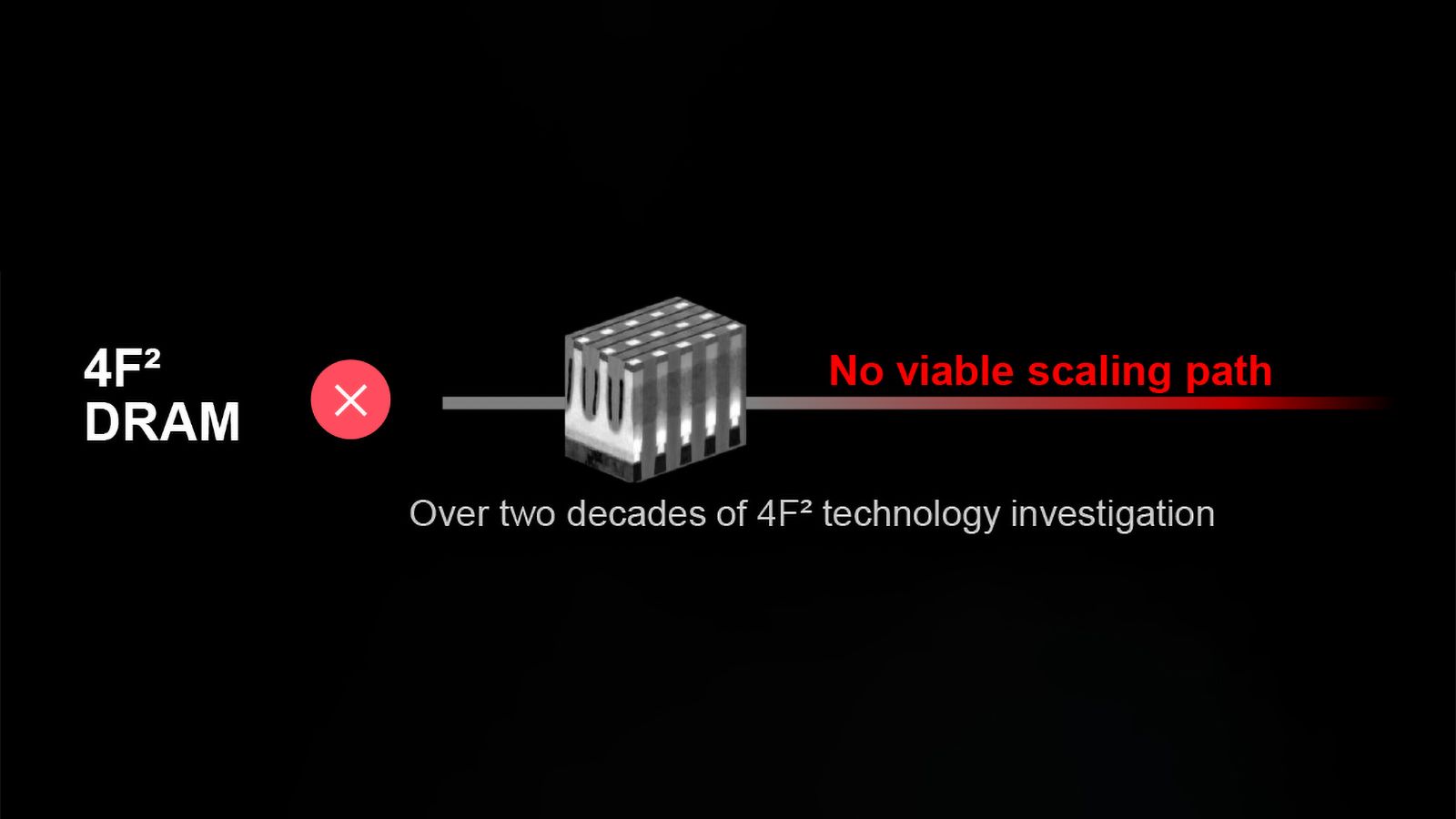
DRAM featuring 4F² memory cells has long been considered one of the holy grails of the DRAM industry, as they promise to reduce cell area by 33% compared with conventional 6F² designs and therefore enable building DRAMs with more memory cells in the same area. However, after working on 4F² memory cells for a couple of decades, Micron has concluded that the architecture offers no meaningful density advantages, increases manufacturing complexity and costs, and has fundamental scaling limitations. This has a dramatic impact on Micron's future plans.
"Micron invented 4F² DRAM," said Scott DeBoer, president and chief technology and products officer at Micron, during the company's event on Wednesday. "The path with 4F² DRAM is always been an option through time, and we have evaluated it and not pursued it due to increased complexity and cost through this past two-decade period of time."
Interestingly, both Samsung and SK hynix still have 4F² memory cells in their roadmaps (according to TechInsights), so Micron's rejection of the technology puts the company on a unique trajectory. Several years ago, the company delayed integration of EUV lithography into its manufacturing flow, contrary to what its rivals did, and still managed to retain competitive positions both in terms of costs and in terms of performance. Therefore, skipping 4F² memory cells is not completely surprising.
4F² is not the future of Micron's DRAM
The main attraction of 4F² DRAM is its theoretically smaller memory cell. The 4F² naming refers to a cell area equivalent to four times the square of the minimum lithographic feature size (F), compared with six times F² for conventional DRAM.
At identical feature dimensions, a 4F² cell occupies approximately 33% less area than a 6F² cell, which could theoretically increase the number of memory cells per wafer by 50%. Such an improvement would reduce manufacturing costs per bit and increase per-device memory capacity even without an equivalent reduction in feature dimensions. However, to make these advantages possible, DRAM makers must develop a suitable transistor architecture and a sufficiently compact capacitor arrangement. This is not easy at all.
(Image credit: Micron)
The CTO of Micron says that the theoretical advantages of 4F² DRAM do not necessarily translate into higher memory density in practice. DeBoer explained that dimensions and pitch of DRAM capacitors, rather than the nominal area of DRAM transistors, ultimately determine how many memory cells can fit on a wafer. Both 4F² and 6F² transistor structures must fit beneath the capacitors, which means that reducing transistor area alone does not guarantee a corresponding reduction in overall cell size because transistors need a capacitor. Furthermore, Micron believes that 4F² introduces additional manufacturing steps and complexity that increase costs without delivering sufficient benefits.
"It is important to understand the capacitor pitch, the capacitor size, and dimensions, is what sets the DRAM bit density, not whether it is 6F², 4F², 8F²," DeBoer said. "From our investigation of this technology over the past couple of decades, it is a bit of a myth that 4F² actually provides anything versus 6F². It is capacitor pitch that defines the DRAM. You can build the cells, the transistors underlying them in different ways, but they still have to fit under the capacitor pitch, which sets the DRAM [cell size]. So, some of that is just smoke and mirrors in terms of talking about 6F² versus 4F²."
4F² memory cells may curb new process technologies
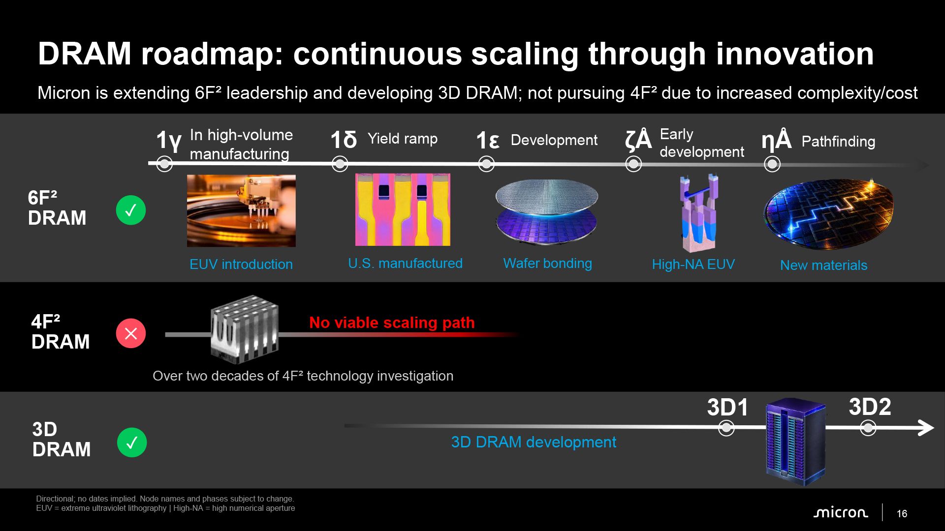
Instead of adopting the 4F² DRAM cell architecture, Micron plans to continue scaling conventional 6F² DRAM. The company believes it can increase bit density by reducing capacitor pitch and shrinking process technologies even without introducing a fundamentally different transistor architecture.
Advanced lithography, new materials, and wafer bonding should allow Micron to extend planar DRAM scaling for several more generations, according to the company. For example, its upcoming 1δ process technology, scheduled to enter volume production in the second half of 2027, promises a mid-20% improvement in bit density compared with its predecessor. Micron also plans to adopt High-NA EUV lithography for future DRAM generations.
(Image credit: Micron)
Interestingly, DeBoer fully acknowledges that 4F² DRAM is technically feasible and that Micron itself has manufactured experimental devices based on the architecture. However, its manufacturing complexity and costs become increasingly problematic as feature dimensions shrink, so essentially Micron claims that it can either adopt 4F² or use more sophisticated process technologies, a claim that perhaps implies why China-based CXMT recently praised 4F². Although DeBoer did not identify any specific physical limitations involved, he stated that 4F² has no sustainable scaling path beyond a certain point. This suggests that Micron sees little value in introducing an intermediate architecture that would eventually require another major transition.
"When you look at a scaling path, you can go back a few nodes and absolutely, 4F² can be built back a few nodes, no question about it," DeBoer noted. "It is more complicated, it is more complex, it is more costly, but you can do that. When we look at scaling 4F² beyond where we are sitting today, there it is; it is physics. There are fundamental problems with 4F² scaling that ultimately will lead to 3D DRAM coming in instead of 4F²."
3D DRAM is the future
Indeed, Micron's preferred long-term solution is 3D DRAM, which would increase memory density by stacking memory cells vertically rather than relying exclusively on reductions in their lateral dimensions. Alongside development of multiple next-generation planar DRAM process technologies, the company is already developing multiple generations of 3D DRAM production nodes (which is not surprising, as 3D NAND nodes will rely on fundamental innovations developed for planar processes), although it has not disclosed when the new architecture will enter commercial production. DeBoer indicated that Micron will make the transition when 3D DRAM offers the right combination of density, manufacturing complexity, and cost.
Although both Samsung and SK hynix have 4F² DRAM products in their roadmaps, Micron believes that the assumption that reducing the nominal footprint of DRAM cells improves manufacturing economics is wrong and that extending 6F² scaling and eventually adopting 3D DRAM offers a better long-term strategy.
In a world where SSDs with up to 256TB capacity are about to enter the scene to compete against hard disk drives that store over 40TB, magnetic tape storage may seem archaic. However, the 25-year-old Linear Tape-Open (LTO) format continues to evolve at a rather impressive pace.
The current LTO-10 generation stores up to 40TB of uncompressed data per cartridge, while HPE, IBM, and Quantum — the companies behind the LTO Program — now envision LTO-14 cartridges with up to 365TB of native capacity. But capacity is not the only advantage of LTO. In fact, the consortium has deliberately slowed its capacity roadmap in a bid to prioritize reliability, cost per terabyte, and manageable backup and recovery times over the previous goal of doubling capacity with every generation.
LTO began in 2000 with the LTO-1 format, which stored just 100GB of data natively and transferred it at 20 MB/s. Since then, capacity increased to 200GB with LTO-2, 400GB with LTO-3, 800GB with LTO-4, 1.5TB with LTO-5, 2.5TB with LTO-6, 6TB with LTO-7, 12TB with LTO-8, and 18TB with LTO-9.
The original LTO-10 media introduced in 2025 increased native capacity to 30TB, whereas an extended-length LTO-10 cartridge announced later increased it further to 40TB.
LTO cartridge capacity has increased by a factor of 400 in about 25 years without changing the form-factor itself. For comparison, the capacity of 3.5-inch hard drives increased by roughly 585 times over the same period, from around 75GB in 2000 to as much as 44 TB today, so tape has evolved at a slower pace. However, LTO has evolved without dramatic changes in internal complexity.
Two scaling vectors
The 40TB LTO-10 cartridge is noteworthy because its additional capacity is enabled by higher recording density and literally longer tape. The LTO-10 format uses 15,104 data tracks (enabled by the new barium ferrite recording layer), up 68.5% from 8,960 tracks with LTO-9, and combines them with higher linear density. To make this possible, LTO-10 uses a redesigned high-bandwidth servo system with a low-mass mechanism that enables the head to follow increasingly narrow tracks accurately, including in environments subject to shock and vibration.
Both 30TB and 40TB LTO-10 media use a strontium-doped barium ferrite (BaFe) recording layer, but the 40TB version uses a new Aramid base film that is thinner and smoother and therefore enables manufacturers to put more tape into the same cartridge. According to MagStor, the thinner substrate increases tape length from approximately 1,035 meters with the 30TB cartridge to around 1,335 meters with the 40TB version. Meanwhile, the 40TB cartridge works with the same LTO-10 drives as the existing 30TB media.
Therefore, modern LTO has at least two major scaling vectors: manufacturers can record more bits on a given area of tape, and can put more tape into a cartridge. Meanwhile, with LTO-10, the consortium had to drop backwards compatibility, which we will detail further within this article.
There appears to be plenty of room left on the tape front. Back in 2020, IBM and Fujifilm demonstrated a strontium ferrite tape technology with an areal density of 317 Gb/in², which they said could theoretically enable a cartridge capable of storing 580TB. The prototype used tracks only 56.2nm wide and a 29nm TMR read sensor, which proved that magnetic tape could reach capacities vastly beyond commercially available LTO products.
Capacity is not everything
Ironically, despite considerable technological headroom, the LTO Program has recently made its roadmap considerably less aggressive.
When HPE, IBM, and Quantum extended the roadmap through LTO-14 in 2022, they expected capacity to roughly double every generation. The plan envisioned 72TB for LTO-11, 144TB for LTO-12, 288TB for LTO-13, and a whopping 576TB native — or 1.44PB compressed — for LTO-14. But that changed in November 2025, when the three companies introduced the new roadmap for LTO that significantly slows down capacity scaling. The current roadmap targets 70TB native for LTO-11, 120TB for LTO-12, 210TB for LTO-13, and 365TB for LTO-14.
While the new roadmap is somewhat less impressive, it does not necessarily indicate that tape technology has encountered a physical scaling wall. The developers claim the revised targets are intended to prioritize reliability, affordability, efficiency, and cost per terabyte. The consortium also specifically says that lowering maximum cartridge capacities should help reduce the amount of time required to store and recover data, which is a legitimate argument even though it looks like an attempt to make a 'feature' out of a limitation.
"AI has turned archives into strategic assets," said Stephen Bacon, Vice President, Data Protection Solutions Product Management, HPE. "The new 40 TB LTO-10 cartridge will help enterprise-class organizations — across healthcare, financial services, media, research, manufacturing, the public sector and beyond — consolidate petabytes efficiently, strengthen cyber resiliency with true offline air-gapping, and keep long-term retention affordable and sustainable."
Bandwidth is becoming one of tape's more obvious limitations. LTO-8 offered 360 MB/s of native bandwidth, LTO-9 increased this to 400 MB/s, and LTO-10 remains at 400 MB/s, although hardware compression can boost effective throughput to as much as 1,200 MB/s when data can achieve the assumed 2.5:1 compression ratio.
As a result, while maximum native cartridge capacity increased from 12TB with LTO-8 to 40TB with LTO-10 — a 3.33X increase — native transfer performance improved by only around 11%. At 400 MB/s, writing 40TB sequentially would theoretically take around 28 hours (without the overheads). Future LTO generations will likely increase performance, but the consortium has not yet published transfer rate targets for LTO-11 and its successors.
No backwards compatibility
One thing to note about LTO-10 is that it has broken a long-standing LTO tradition, which is backward compatibility. Up until LTO-7, new drives could generally read cartridges from two generations earlier and write media from one generation earlier. LTO-8 and LTO-9 reduced compatibility to one previous generation. However, because LTO-10 redesigns its head, its backwards compatibility disappears completely: an LTO-10 drive reads and writes only LTO-10 media, although the 30TB and 40TB cartridges are of course interchangeable.
This creates a natural problem for operators that need to maintain archives for decades. Once they adopt LTO-10, they either must migrate all their archives to the new format from LTO-8 or LTO-9 cartridges, or keep the old drives in their fleet, which may be increasingly difficult.
Demand remains strong
Perhaps counterintuitively, the AI boom could strengthen demand for tape. AI infrastructure produces enormous datasets, but not every training dataset, checkpoint, model, log, or generated asset needs to remain indefinitely on expensive SSDs or HDDs.
LTO capacity shipments reached 160.3 exabytes in 2025, down 9% year-over-year. However, shipments in the first quarter of 2026 jumped 57% YoY, according to figures reported by the LTO consortium. The organization attributed the increase to AI-related data growth, traditional archival demand, cyber-resilient backups, continued LTO-9 adoption, and the beginning of the LTO-10 transition.
"We are seeing unprecedented data growth combined with increasing cost, energy, and cyber resilience pressures across the industry," said Hugues Meyrath, CEO, Quantum. "As organizations adapt to this new reality, tape is increasingly viewed as a strategic component of modern data infrastructure, delivering predictable economics and resilient long-term data retention at scale."
Indeed, tape has a number of fundamental advantages that are not going to disappear any time soon. Tape provides vast capacities at a low cost per terabyte, cartridges consume virtually no power while sitting offline, hardware encryption protects data, and physically removing a cartridge from a drive provides a genuine air gap against network-based attacks. LTO also supports the LTFS file system, which maintains indexing information on tape and makes archived files considerably easier to manage.
Meanwhile, tape's disadvantages are equally fundamental and are not going away: tape is sequential and therefore cannot provide anything resembling the random-access performance of HDDs or SSDs. Although nobody expects something similar from it.
LTO isn't going anywhere
25 years after LTO-1 offered 100GB per cartridge, LTO-10 can store as much as 40TB, and the roadmap calls for 365TB with LTO-14 several years down the road. Perhaps more importantly, laboratory demonstrations indicate that magnetic tape itself has considerable scaling potential beyond today's commercial products. Meanwhile, instead of pushing capacity as quickly as technologically possible, the LTO consortium is now deliberately balancing density with reliability, performance, and cost.
For a storage technology which demise has been predicted repeatedly for decades, LTO not only continues to evolve at a predictable pace, but its adoption is growing, while its relevance remains on a high level. Only time will tell whether it remains relevant for another quarter of a century, but its steady progress certainly increases this possibility.
Intel on Wednesday announced that it had started installing production tools at its Fab 62 in Arizona, and the fab is on track for mass production by late 2028. The company also reported progress on its Ohio One manufacturing complex and confirmed that it has integrated High-NA EUV lithography into high-volume manufacturing (HVM). Meanwhile, Intel continues to invest in its leading-edge process technology R&D, advanced packaging, and photomask production capabilities in the U.S., which puts the company ahead of the competition.
"There is an important difference between technologies made in America and technologies that are truly American-made," wrote Naga Chandrasekaran, executive vice president and chief technology and operations officer, Intel Foundry. "The difference lies in the research and development process that transforms ideas into manufacturable technologies."
Fab 62 to begin operations in 2028
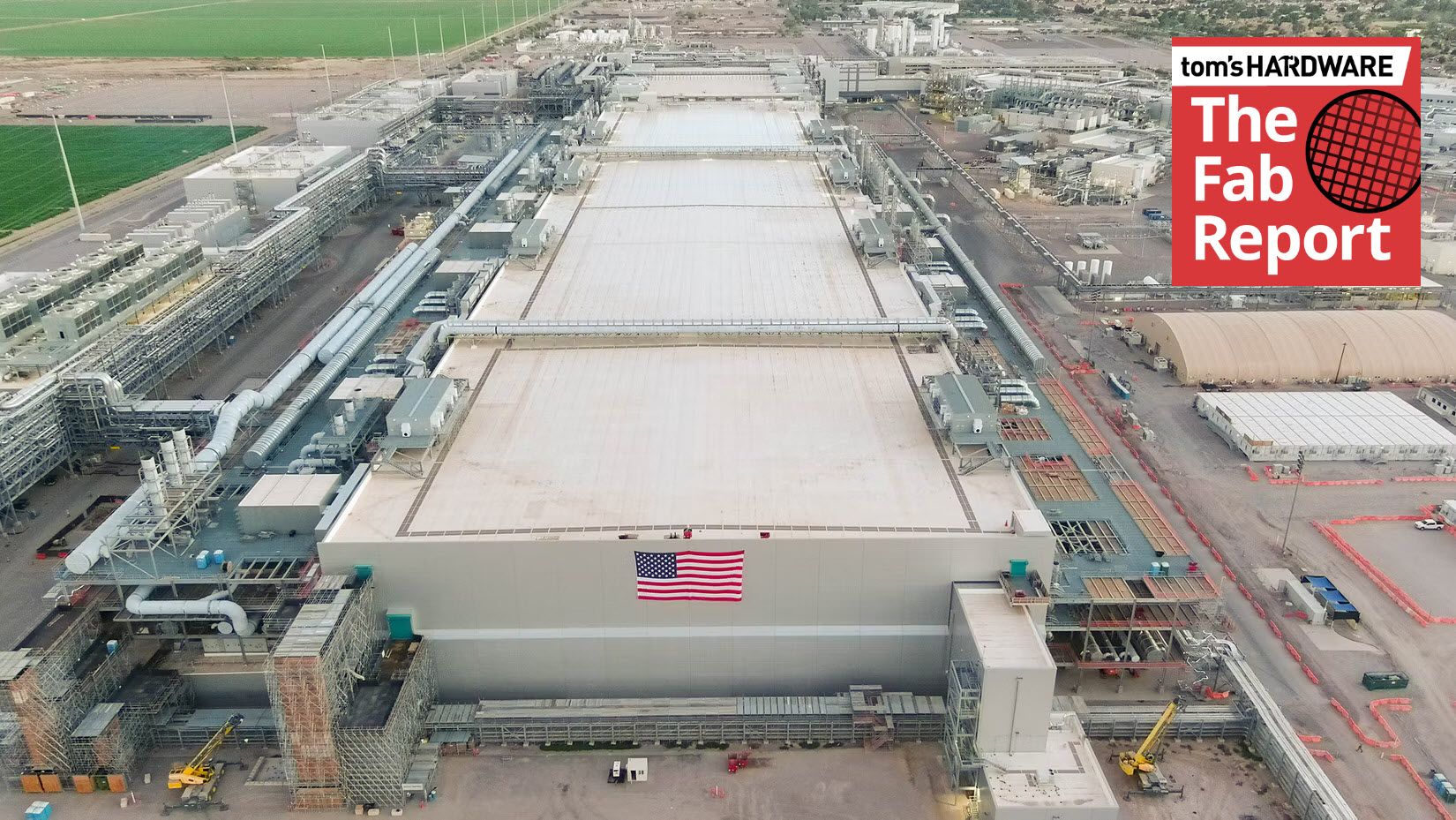
Intel completed construction of its Fab 62 shell some time ago; now it is time for the company to begin installing production tools, which is what it is doing now. Intel expects the new facility to become operational before the end of 2028, although it has not disclosed when it intends to begin high-volume production or which nodes it will produce.
(Image credit: Intel)
Intel has not officially assigned Intel 14A to Fab 62, although the facility has been discussed as a potential manufacturing site for the node. Meanwhile, there is an important distinction between Intel's original plans for Fab 62 and its current commitments. When Intel announced Fab 52 and Fab 62 in Arizona, it said the two facilities would manufacture its most advanced process technologies, including Intel 20A (2nm-class) and 18A (1.8nm-class). Intel subsequently designated Fab 52 for Intel 18A manufacturing. Yet, Fab 62 remains unassigned.
Given Intel's manufacturing process roadmap disclosed earlier this year, Fab 62 will be able to make chips on 18A, 18A-P, and 14A nodes. Intel currently manufactures Intel 18A chips at the neighboring Fab 52, whereas Fab 62 could potentially accommodate either additional Intel 18A capacity or the company’s next-generation Intel 14A process technology. However, Intel has yet to confirm its plans for the facility.
The facility will become Intel's Fab 62, the sixth high-volume semiconductor manufacturing fab at its Ocotillo campus, which has served as one of the company’s primary production sites for decades.
Intel has also not revealed Fab 62's planned wafer processing capacity, or the amount of capital expenditures required to complete the facility. Nevertheless, the installation of production equipment indicates that the project has progressed beyond construction of the building itself. The new fab will expand Intel’s manufacturing footprint in Arizona, where the company already produces leading-edge processors and operates advanced packaging, assembly, and testing facilities.
Intel confirms High-NA EUV insertion into mass production
Another noteworthy disclosure concerns Intel's deployment of High-NA EUV lithography. Intel was the first chipmaker to install a commercial High-NA EUV scanner at its D1X fab near Hillsboro, Oregon, and subsequently integrated the tool into high-volume manufacturing to produce its Panther Lake and other chips.
The Gordon Moore Park at Ronler Acres in Oregon is where Intel develops its most advanced logic process technologies and initiates volume production of the latest processors. Usage of High-NA EUV to produce select tiles for Panther Lake CPUs at D1X is a natural fit for the development fab, as it helps Intel to better understand how these lithography systems work. Meanwhile, it seems (though Intel has not explicitly confirmed) that, for now, High-NA EUV scanners are used to produce the same circuits as Low-NA EUV machines, so the use of next-generation lithography systems does not necessarily provide significant advantages over existing litho scanners.
Ohio One reaches another construction milestone
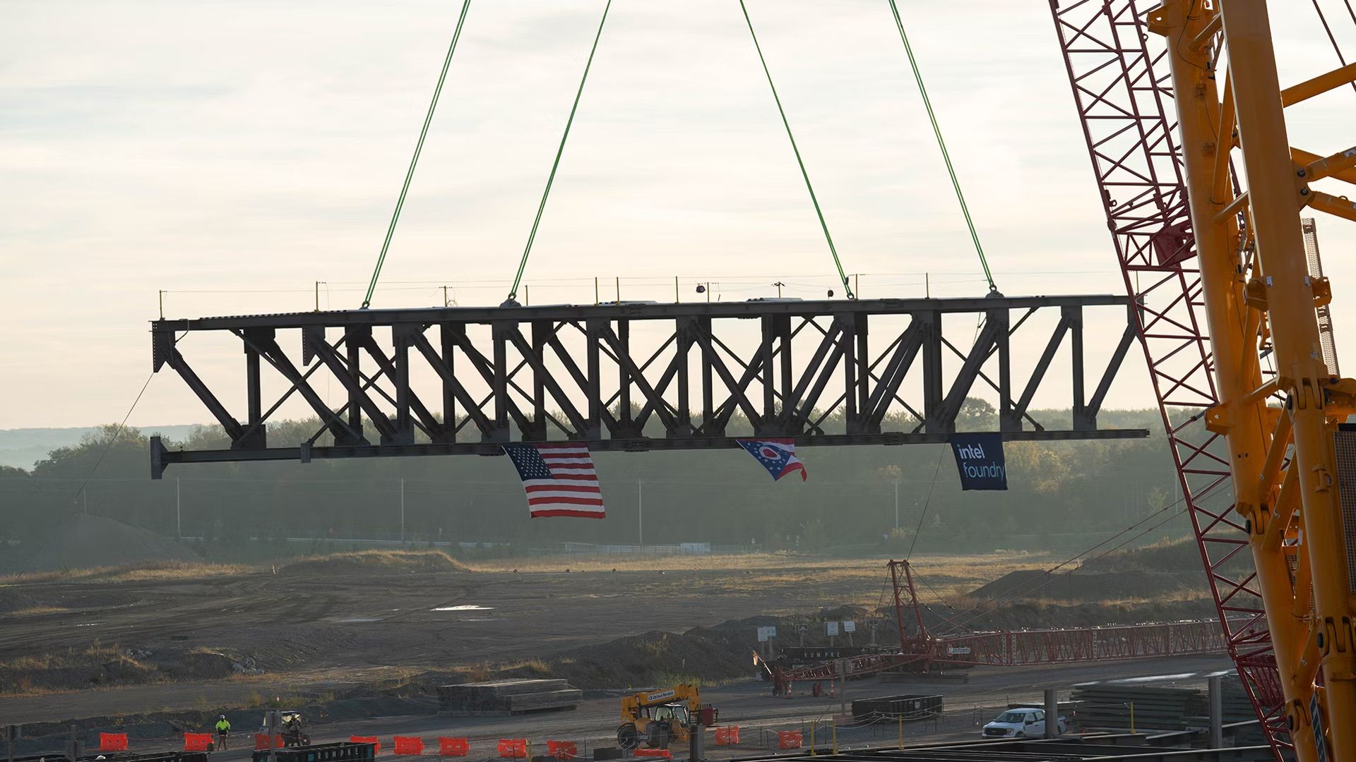
Intel has also made progress with its 'Ohio One' manufacturing complex in New Albany, Ohio. Construction workers recently installed the first major structural truss at the site's first semiconductor fab, which represents a milestone in the development of the company's manufacturing operations in the state. The project is clearly an important part of Intel's long-term strategy to expand domestic production of chips using leading-edge process technologies for years to come.
(Image credit: Intel)
Unfortunately, Intel did not provide an updated construction schedule for Ohio One or disclose when the first fab is expected to begin operations. Intel also did not reveal which process technology the facility will eventually use or the estimated manufacturing capacity it will provide. Therefore, while construction continues, which is good news, the announcement does not clarify exactly when Ohio One will contribute to Intel's output.
Other investments across the U.S.
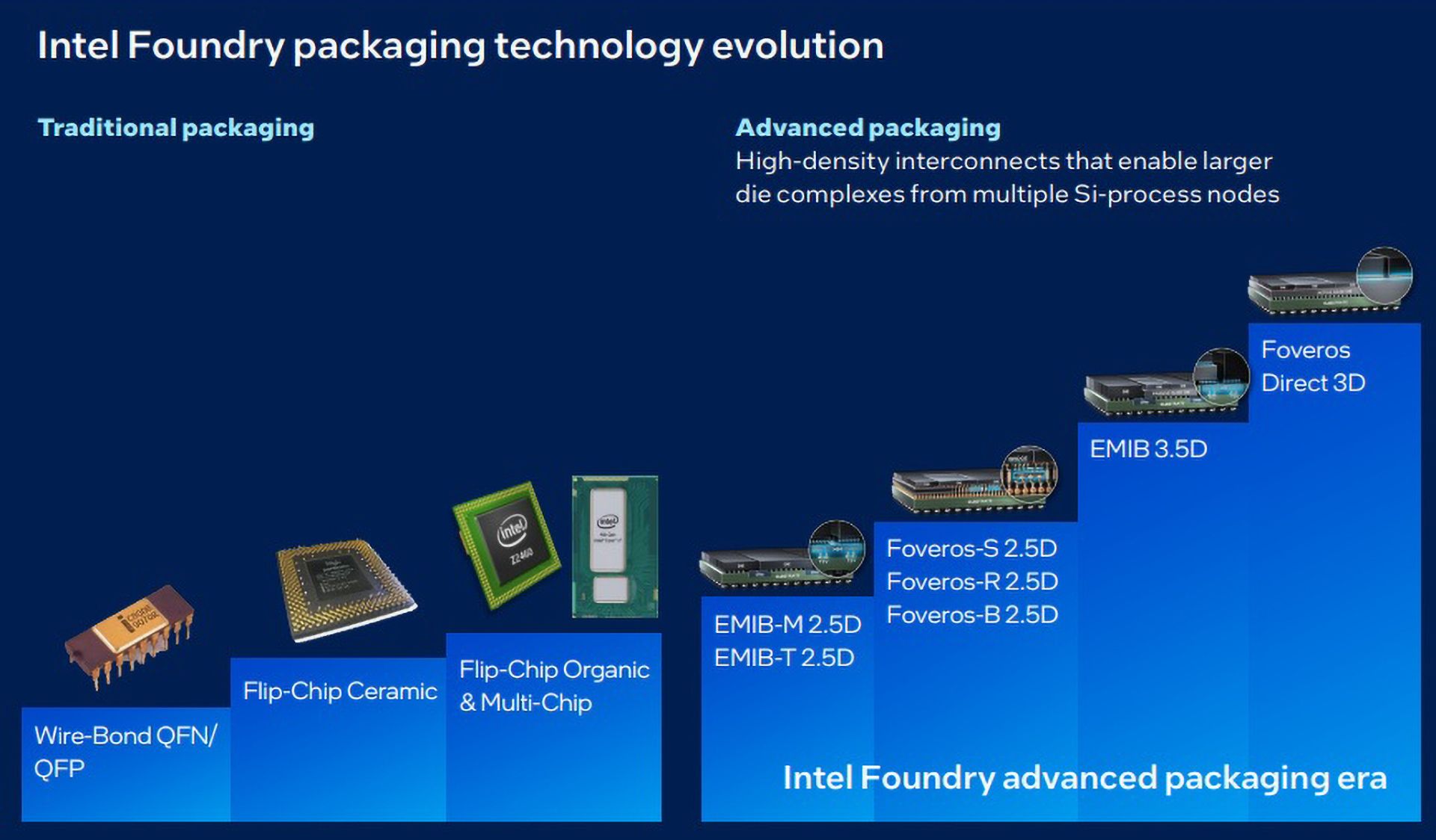
In addition to leading-edge manufacturing capacity in the U.S., Intel continues to invest in advanced packaging technologies. Oregon serves as the company's main research and development center for advanced logic and 3D interconnect technologies, while Arizona hosts advanced packaging R&D, assembly, and testing operations. Intel uses its site in New Mexico to produce its complex multi-chiplet processors relying on advanced packaging methods — starting with modest EMIB and all the way to next-generation EMIB-T and Foveros technologies.
(Image credit: Intel)
Also, Intel recently broke ground on a new photomask manufacturing facility in Santa Clara, California. The new facility will be an important part of Intel's supply chain in the U.S., as the company will be the only chipmaker in America to develop and produce chips using leading-edge nodes completely in the U.S. (both Samsung and TSMC currently lack leading-edge process R&D in America; they do not run their own photomask shops in the U.S., and Samsung has abandoned its plan to build an advanced packaging facility in Texas). Of course, Intel critically depends on tools from Europe and materials from Japan, but even as its major rivals invest hundreds of billions in their U.S. production capacity, Intel remains ahead.
To highlight its American supply chain, Intel disclosed that its U.S. operations involve more than 4,500 suppliers across 49 states, as its annual domestic expenditures exceed $29 billion. The company stressed that domestic semiconductor leadership requires not only wafer fabrication capacity but also research, process development, advanced packaging, and a comprehensive supply chain.
Micron faces a one-day labor stoppage at its Taoyuan operations in Taiwan on October 22, Reuters reports. Micron's employees are striking for concrete terms for this year's bonus and a clearer mechanism for sharing the company's future profits. The strike's teeth come from the resultant financial impact on Micron's operations, as semiconductor fabs are supposed to operate around the clock. The scheduled protest comes amid strong demand for memory chips and will have a minor impact on Micron's memory output.
The Taoyuan union wants Micron to present a specific proposal for this year's additional employee bonus and establish a transparent formula for distributing a portion of future profits. Previous negotiations between the company and the union ended unsuccessfully in September, which prompted employees to approve industrial action in early October. Nonetheless, the union stresses that the October 22 strike is intended to pressure Micron into reaching an agreement rather than terminate negotiations. The union is prepared to conclude a deal if the company presents terms acceptable to employees across its Taiwanese operations.
The situation could become more serious if employees at Micron's Taichung operations, its largest manufacturing site in Taiwan, decide to join the action. A separate labor organization that represents workers at that facility is scheduled to meet with Micron for mediation on October 22, the same day as the Taoyuan protest. However, the Taichung union has not yet authorized a strike.
Micron's fabs in Taiwan produce commodity DDR5 and LPDDR as well as expensive high-bandwidth memory (HBM) for AI accelerators. Amid record demand for memory of all types, even a one-day suspension of operations would have a material impact on Micron's output and earnings.
Modern semiconductor fabs are supposed to work 24/7/365, as many processes cannot be halted. However, if management has sufficient time and personnel to prepare, a one-day warning strike does not necessarily mean a complete shutdown of Micron's Taoyuan manufacturing operations, not to mention permanent damage to wafers or equipment. The actual consequences of the strike will depend on employee participation, which manufacturing operations are affected, and Micron's contingency plans. While it is likely that the output will drop, the decline will likely be negligible.
Micron employs approximately 15,000 people in Taiwan. The workers point to compensation arrangements at Samsung Electronics and SK hynix as examples of how semiconductor manufacturers can distribute profits among employees as AI-driven demand generates unprecedented cash flows for memory firms.
Nvidia has earned billions selling AI accelerators, but with the emergence of agentic AI, CPUs are going to play a considerably more significant role than before, which creates new opportunities for the company. Reutersreports that Nvidia has secured a major design win with its Vera CPUs with AI cloud provider Modal. According to Modal, preliminary evaluations showed that Vera could deliver twice the throughput of its existing AMD and Intel processors, although the company does not intend to cease using CPUs from its current suppliers.
Modal provides cloud infrastructure that enables AI developers to deploy AI agents that can perform complex operations autonomously over extended periods. Such workloads require substantial CPU resources for software execution, data processing, and other tasks that cannot be efficiently handled by GPUs. Modal currently relies exclusively on AMD and Intel processors for these operations, but its tests indicate that Nvidia's new Vera CPUs could significantly improve performance in its specific workloads. Of course, since Vera is based on an Arm instruction set architecture, Modal's decision to adopt Vera will require substantial modifications to its software. Nevertheless, Modal believes that the potential performance improvements justify the additional engineering effort.
The reported 2x throughput advantage is particularly interesting because agentic AI workloads can involve numerous independent tasks that compete for CPU cores, cache capacity, and memory bandwidth. However, Modal has not disclosed detailed benchmark configurations it used, specific AMD and Intel processor models, or performance-per-watt figures. Consequently, it remains unclear whether Vera's advantage is enabled by advantages of its Arm v9.2-based Olympus CPU cores that can decode and execute up to 10 instructions per cycle, its memory subsystem with 1.2 TB/s of bandwidth, or other architectural characteristics. Also note that tests compared Vera against currently available AMD and Intel processors rather than their upcoming generations that will compete against Vera in the coming years.
Since Modal cannot port all of its software to Arm ISA overnight, the company will continue using x86 CPUs from AMD and Intel, according to Modal chief executive Erik Bernhardsson. Rather than sticking to one ISA for everything, Modal intends to operate a heterogeneous server fleet and select the most suitable processors for each workload. Naturally, the company intends to evaluate upcoming AMD and Intel processors once they become available to make its choices in the future.
For Nvidia, the agreement represents a major step toward making Vera a standalone server processor that commands a major share of the server market. The company expects Vera sales to generate at least $20 billion during its current fiscal year and estimates the potential total available market for these CPUs is approximately $200 billion. The company is on track to sell at least four million Vera CPUs in fiscal 2026.
The announcement comes shortly after Modal secured $750 million in financing led by Accel, which valued the company at $15.75 billion. Modal expects its annual revenue to reach $1 billion within the next year. The company's service consumption has increased 3X in the last 12 months, while revenue has surged more than 15 times compared with the previous year, Reuters reports.
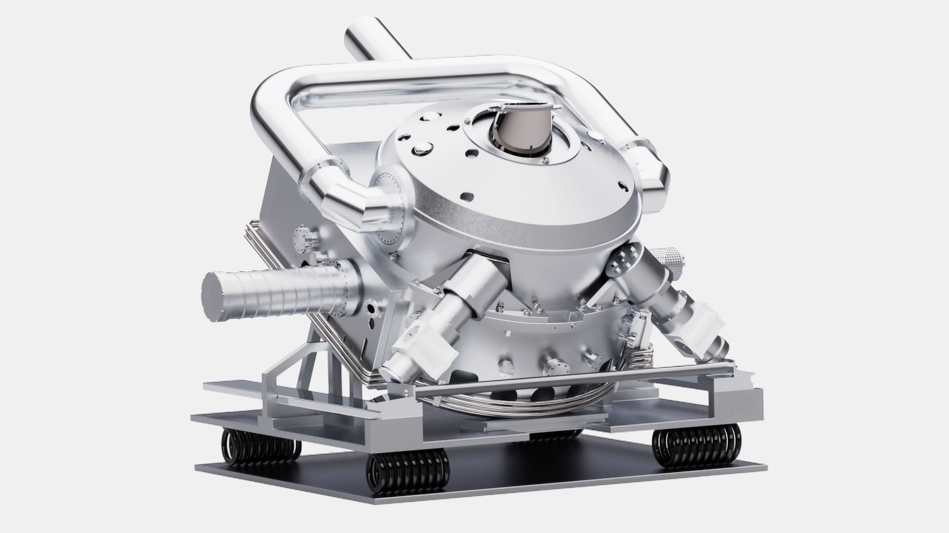
Being unable to procure EUV litho tools from ASML, China must develop such systems locally, so from time to time we learn about an EUV-related 'breakthrough' in China that will turn into an actual EUV scanner over the following several years. This week, Chinese startup Langdao Silex demonstrated a prototype extreme ultraviolet (EUV) light source with over 15W of output power, 90% domestic components, and decent uptime. The company will need another three to five years to commercialize its technology, reports TrendForce, citing various sources. Yet, a light source alone does not make an EUV scanner.
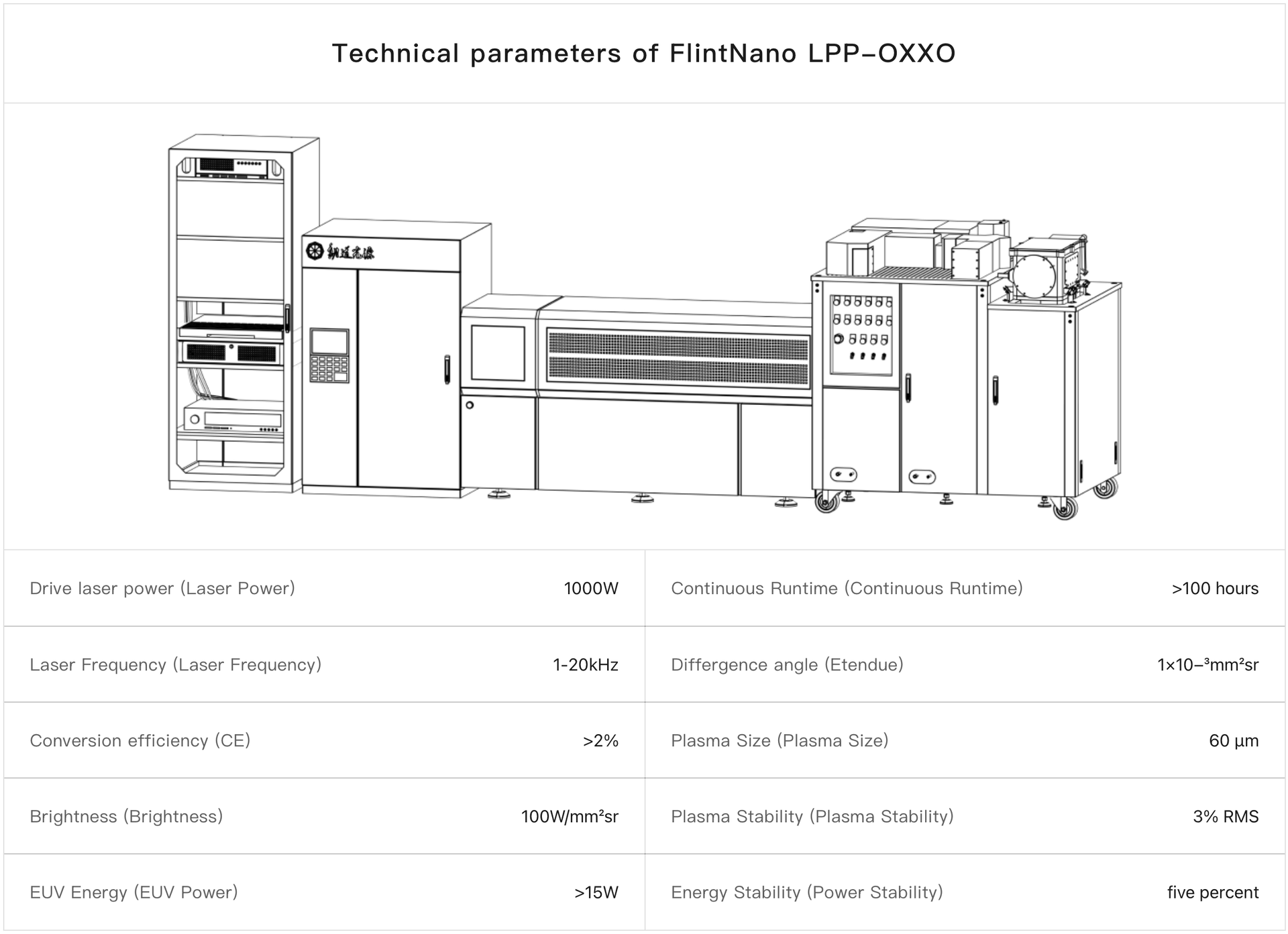
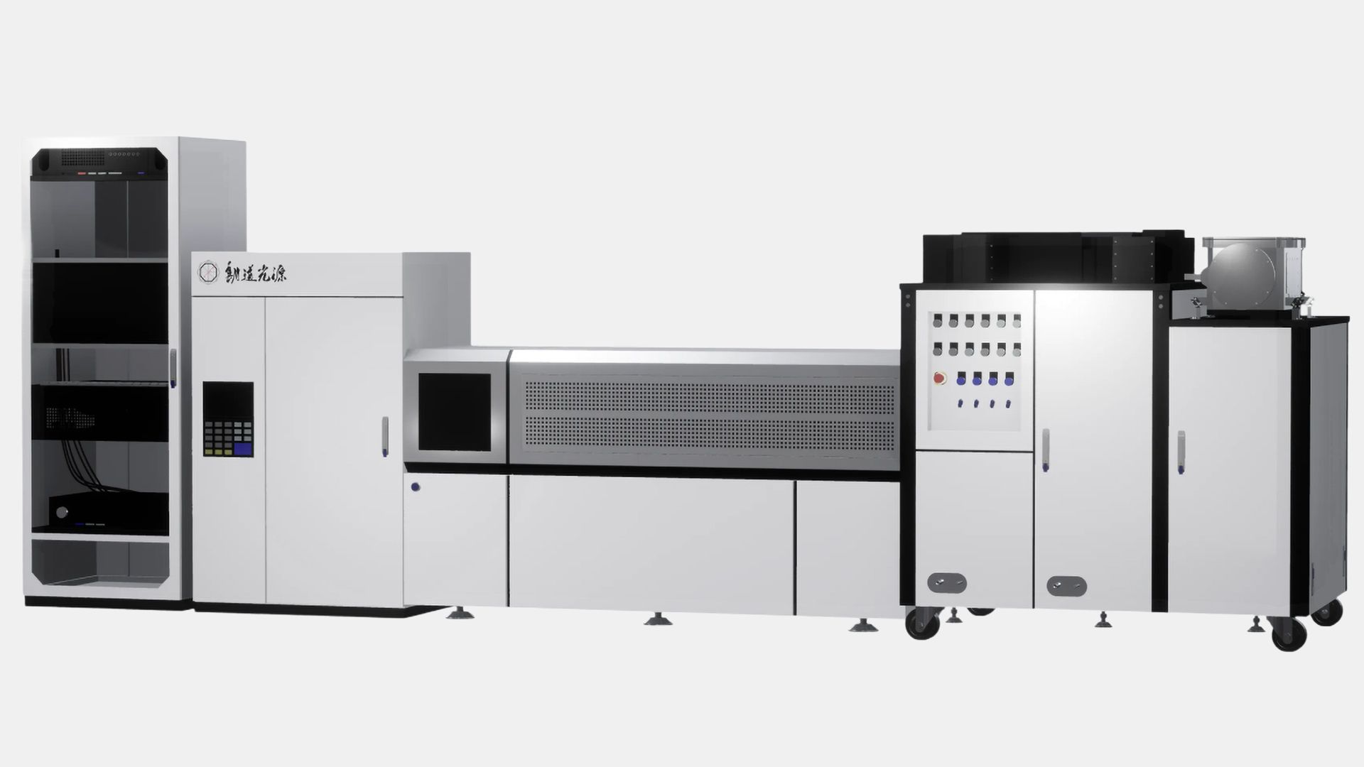
Langdao Silex, which was established in 2024 by Tsinghua University's Gas Discharge Plasma Laboratory alumni, demonstrated its EUV light source prototype at the 26th China International Industry Fair in Shanghai, for obvious reasons, without lighting it up. Just like modern light sources from ASML, the company's low-power FlintNano LPP-OXXO system uses laser-produced plasma (LPP) technology that produces EUV radiation by bombarding tiny heated metal droplets with high-energy laser pulses to create extremely hot plasma. The system features a 1,000W driving laser (presumably a CO2 one) with an operating frequency of 1 kHz – 20 kHz and conversion efficiency exceeding 2%. Its EUV output exceeds 15W (presumably measured at the plasma rather than at intermediate focus, as the company has not demonstrated a complete EUV collection system) while its brightness reaches 100 W/(mm²·sr). The source has an étendue of 1 × 10⁻³ mm²·sr and generates plasma with a diameter of 60 μm.
(Image credit: Langdao Silex)
According to Langdao's specifications, the FlintNano LPP-OXXO can operate continuously for over 100 hours with plasma stability of 3% RMS and EUV output power stability of 5%. These characteristics make the system suitable for semiconductor exposure experiments, although its output remains insufficient for high-volume chip production. Meanwhile, the 'over 100 hours' availability is very impressive for a pre-production light source, though we must admit that there is no way to verify the claim.
Langdao is also developing the FlintMicro-LPP high-power EUV source, which has completed proof-of-principle validation, according to reports. However, Langdao has not disclosed its output power, conversion efficiency, or operating lifetime.
On paper, Langdao's EUV source is comparable in output to some of the earliest EUV sources developed by Western and Japanese equipment makers, albeit with a major caveat: Langdao seems to measure EUV power at the plasma rather than after the collector or at intermediate focus as ASML does. ASML's early EUV demonstration equipment used approximately 10W at intermediate focus DPP sources in 2007, while Cymer's LPP sources installed in early NXE:3100 systems delivered up to 11W during wafer exposure in 2012 (note that ASML's machines are source agnostic, so some NXE:3100 prototypes used DPP sources, while others used LPP sources). By 2013, Cymer demonstrated approximately 40W at intermediate focus over extended operating periods. Meanwhile, Japan's Gigaphoton targeted 25W with its first prototype in 2013 and demonstrated 43W in early 2014. By late 2014, Gigaphoton had achieved 118W during a 10-minute test. However, since these historical figures involve different measurement conditions and operating durations, direct comparisons are vastly inaccurate.
Not quite there
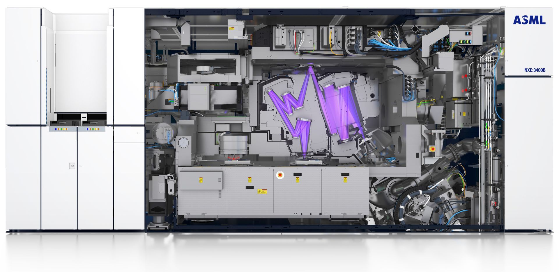
Langdao Silex has not demonstrated its EUV light source in action, so all we know about it comes from the company itself. As noted, 15W power looks comparable to early EUV sources developed by Philips Extreme UV (DPP) and Cymer (LPP). Meanwhile, early NXE:3400-series machines came with 125W – 150W at intermediate focus sources, which was far from enough for high-volume manufacturing (HVM).
(Image credit: Langdao Silex)
Modern EUV lithography equipment comes with considerably more powerful sources. ASML introduced 250W-class EUV sources for commercial production in 2018 – 2019 and has since achieved substantially higher output levels. Increasing output requires more powerful CO₂ lasers, highly accurate tin-droplet generators, effective debris mitigation, durable collector mirrors, and considerably better long-term reliability.
Langdao claims that 90% of its prototype's components are domestically sourced and that most critical parts were developed in China. However, the company has not explained whether the localization figure reflects component count, value, or another metric. Furthermore, its representatives reportedly acknowledged that increasing EUV output and improving long-term operational stability are the targets to be achieved in a bid to commercialize the source.
Not an EUV scanner
Yet, even without complete EUV scanners, Langdao's source could support EUV photoresist development, mask inspection research, development of EUV collection and illumination optics, and eventually experimental exposure testing.
Developing a complete EUV lithography scanner will require further advances in EUV collection and illumination systems, high-precision multilayer mirrors, wafer and reticle stages, overlay accuracy, and system integration. Meanwhile, all of these devices require a separate supply chain that hardly exists in China today.
Therefore, even if Langdao successfully develops its EUV source and increases its output to levels suitable for high-volume manufacturing, this would not necessarily mean that China could manufacture its own EUV lithography machines any time soon. Moreover, while Langdao's progress is impressive, it took ASML/Cymer approximately six years to increase the output of its LPP EUV source from 11W to 125W – 150W at intermediate focus, so there is no way that Langdao's LPP source could be used for anything beyond development tools in the next three to five years.
Meanwhile, Langdao has not disclosed where its reported 15W of EUV output is measured. If this figure represents radiation generated at the plasma rather than power delivered at intermediate focus, the source's usable output would be considerably lower than 15W when measured according to industry-standard practices. That said, it does not look like China got significantly closer to building its own EUV lithography scanners with the current announcement.
Reports that Solidigm was considering building a 3D NAND fab in the U.S. came as a surprise last month, as no company has manufactured NAND flash memory in America for years. However, the potential investment now appears to be part of a calculated move by Solidigm's parent, SK hynix, which is reportedly asking the U.S. government to authorize additional semiconductor manufacturing equipment shipments to its Dalian facility in China in exchange for a commitment to build a new NAND fab in the U.S., according toReuters.
The Dalian fab is the world's only facility to produce 192-layer floating gate 3D NAND for Solidigm's data center-grade SSDs for AI, enterprise, and hyperscale data centers. Its manufacturing operations rely on equipment from major American suppliers, including Applied Materials, KLA, and Lam Research, whose exports to China require a license from the U.S. government. Although the U.S. authorities tend to authorize shipments of some tools to semiconductor facilities in the People's Republic that are operated by multinational companies like Samsung or SK hynix, they only want to keep the fabs running, as they are against expansions of capacity of fabs in China or introducing new manufacturing technologies to these facilities.
Solidigm has requested U.S. export licenses for additional tools, but the U.S. government has yet to authorize the shipments. Last December, the U.S. Commerce Department granted SK hynix a limited authorization for equipment deliveries to Dalian for 2026, but it has not issued a similar equipment export authorization for 2027, according to Reuters. In a bid to persuade the U.S. government to authorize shipments of necessary tools to its Dalian facility, SK hynix proposes to build a 3D NAND facility in America. This would fill an important gap in the Trump administration’s efforts to bring semiconductor manufacturing back to the U.S.
SK hynix's Solidigm subsidiary wants to install additional manufacturing equipment in the unused portions of its Dalian Mod B facility, which was completed in 2023. The company never fully equipped the building because of the memory market downturn at the time, so while some production tools are installed, substantial space remains unused and is available for additional tools. Given that Solidigm sells every single SSD it produces, unused capacity means lost revenue. Meanwhile, because the building was completed in 2023, installation of tools into that facility does not constitute a capacity expansion.
Additional NAND production in China could generate profits that Solidigm could use to finance its proposed American fab and support its operations until domestic manufacturing capacity becomes available. The company is also considering an initial public offering as early as 2027 to raise additional capital.
Solidigm has previously confirmed its commitment to further development of floating-gate 3D NAND technology. In aninterview with Tom's Hardware at Computex 2026, Avi Shetty, who leads Solidigm's AI solutions and ecosystem business, said that the company intended to develop 5th and 6th Generation floating-gate NAND beyond its existing 192-layer technology. He also emphasized the importance of maximizing factory utilization and profitability. However, he did not disclose plans to expand manufacturing output at the company's Dalian facility, not to mention a new fab in the U.S.
Nonetheless, the new reports about SK hynix's intentions clearly indicate that the company not only intends to keep developing new generations of Solidigm's floating-gate NAND, but also to expand its production in China and the U.S.
ASML this week reported record quarterly revenue of $13.06 billion (€11.66 billion) and profitability of nearly $5.79 billion (€5 billion) as demand for advanced semiconductor manufacturing equipment continues to accelerate and investments in AI infrastructure continue to increase. The company now expects demand for its lithography systems to exceed its production capacity in 2027 and 2028, despite plans to increase output substantially. Some clients are already interested in placing orders for equipment as far ahead as 2030, which makes ASML consider further capacity expansions beyond its previously announced intentions.
Record financial results
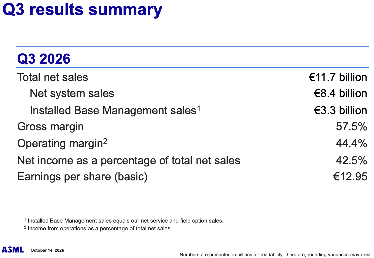
ASML reported third-quarter 2026 revenue of $13.06 billion USD (€11.66 billion), up 55% year-over-year and 25% sequentially. The company's gross margin reached a record 57.5%, up from 51.6% a year earlier, while operating income rose to $5.79 billion (€5.17 billion). Net income reached $5.56 billion USD (€4.96 billion) , although this figure includes approximately $570 million (€510 million) from the re-evaluation of the company's investment in Mistral AI.
(Image credit: ASML)
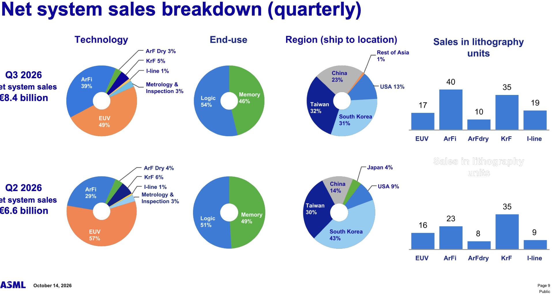
During the quarter, ASML sold 121 lithography systems, including 113 new and eight refurbished machines, up from 91 systems in Q2 2026. The company generated $4.59 billion USD (€4.1 billion) from 17 EUV lithography systems and $4.82 billion USD (€4.3 billion) from 85 DUV (including 45 ArFi scanners) and 19 i-line litho tools. In addition, ASML recognized revenue from one High-NA EUV system in Q2. Of total equipment revenue, 54% came from logic chipmakers and 46% from memory manufacturers.
(Image credit: ASML)
Taiwan accounted for 32% of ASML's equipment sales in Q3 2026, followed closely by South Korea at 31%. China represented another 23%, while the United States accounted for 13% and the rest of Asia contributed just 1%. Combined, Taiwan and South Korea generated 63% of ASML's equipment revenue, which reflects substantial investments in advanced logic and memory manufacturing capacity that by far exceed those in the U.S. and Japan.
(Image credit: ASML)
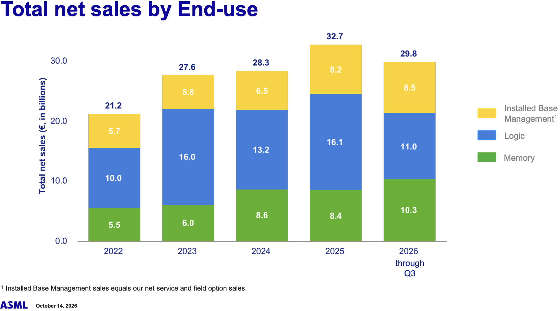
ASML’s Installed Base Management business generated $3.68 billion (€3.29 billion), approximately $450 million (€400 million) above guidance, largely due to strong demand for productivity upgrades (more on this later), which contributed to the company’s record profitability.
For the fourth quarter, ASML expects revenue of $15.9 billion to $17.0 billion (€14.2 billion to €15.2 billion) and gross margin of approximately 57%. Full-year revenue should reach $49.3 billion to $50.4 billion (€44 billion to €45 billion), up approximately 36% YoY. The company projects EUV revenue should increase by more than 45% year-over-year, while memory-related equipment sales are expected to rise by approximately 75%, which indicates growing demand from DRAM producers.
Demand for litho tools spans to 2030
One of the biggest learnings from these results and accompanying statements is that semiconductor manufacturers are increasingly interested in securing lithography equipment years before they actually need it. According to ASML CEO Christophe Fouquet, customers expect demand for its products to exceed available supply through at least 2028, which encourages them to accelerate construction of new fabs as well as expand their existing capacity.
"Our leading-edge high-volume customers are sharing very good visibility as a result of the increasing number of long-term commitments they are securing with their customers," Fouquet said during the company's conference call with analysts and investors. "This extended visibility has led them to conclude that demand for their products will outpace supply through at least 2028. As a result, customers are accelerating capacity build-out plans and preparing for further expansion beyond 2028 in order to better meet the anticipated level of demand."
(Image credit: ASML)
ASML is already receiving orders that are to be delivered in 2028, while some customers have expressed interest in equipment for 2029 and even 2030.
"As customers shift focus to their needs beyond 2027, our order momentum continues to build," Fouquet added. "We are increasingly receiving orders for 2028, and customers are also expressing interest in placing orders for 2029 and even 2030."
To address this demand, ASML plans to manufacture approximately 65 Low-NA EUV systems in 2026, up from 44 scanners shipped in 2025. Production of immersion DUV systems should remain approximately at last year's level, even though proveiously the company expected shipments of DUV tools to decline.
The company previously announced plans to increase production capacity for both Low-NA EUV and immersion DUV systems by 30% in 2027, followed by another potential 30% increase in 2028. Based on its 2026 EUV production target, this implies capacity for approximately 85 Low-NA EUV systems in 2027 and roughly 110 in 2028, assuming both increases materialize.
However, ASML now believes even this level of output will be insufficient and is investigating ways to expand its 2028 capacity beyond the previously planned 30% increase. However, the company has not disclosed revised production targets.
"Looking further ahead, we shared our intent last quarter to increase our capacity in 2027 by 30% for both Low NA EUV and DUV immersion systems, as well as to investigate adding a further 30% in 2028," explained Roger Dassen, Chief Financial Officer at ASML. "However, given the dynamics of this quarter, we now anticipate that our current planned levels of output in 2027 and 2028 will not fully meet the demand of our customers."
High-NA EUV adoption
Meanwhile, High-NA EUV adoption is progressing. Intel has already exposed more than one million wafers using High-NA systems and plans to start using High-NA EUV with its 14A process technology in 2028. Samsung plans to introduce High-NA EUV into high-volume manufacturing (HVM) in 2028 for DRAM and for logic later, while TSMC plans to use High-NA EUV scanners by 2030 – 2031. ASML says availability across its installed High-NA fleet is approaching 90%, which suggests that the tools are becoming mature enough for HVM deployment.
(Image credit: ASML)
Interestingly, Samsung's planned 2028 introduction may create additional demand for High-NA equipment from memory manufacturers, as they will need to compete against their larger rival. However, ASML has not disclosed specific shipment targets for these tools.
New tools, more capacity
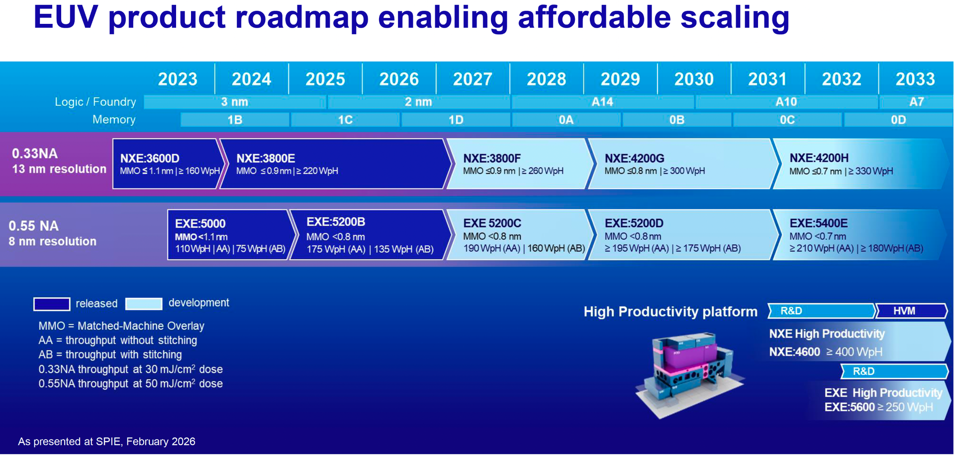
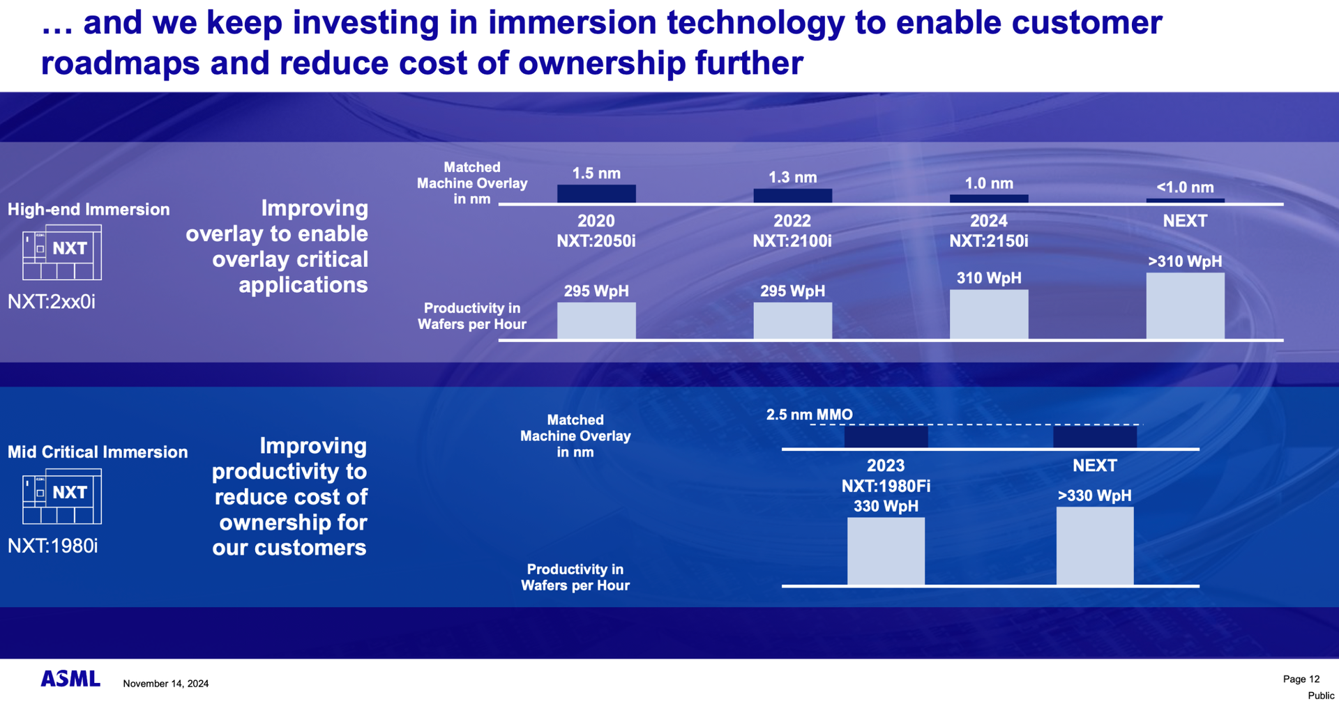
ASML also intends to increase semiconductor production capacity by introducing more productive lithography systems. Its upcoming Twinscan NXE:3800F, scheduled for introduction in early 2027, will process up to 260 wafers per hour, compared with 230 wafers per hour for the existing NXE:3800E. While this represents 'only' approximately 13% higher throughput, this translates to 21,600 extra EUV exposures per month without corresponding increases in cleanroom space. Three such tools per fab enable 90 additional EUV exposures per hour, 2,160 per day, or 64,800 per month. The company also plans to introduce a new critical-layer immersion DUV system capable of processing 330 wafers per hour.
(Image credit: ASML)
Keep in mind that the actual fab capacity improvements depend on the number of lithography exposures required per wafer on a particular node, as well as the capabilities of other manufacturing equipment.
ASMLASML
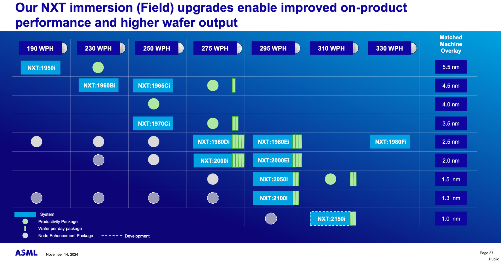
Another important element of ASML's strategy is its growing portfolio of productivity upgrade packages for existing EUV and DUV systems. Such upgrades enable chipmakers to increase wafer throughput without purchasing additional scanners, which can provide additional capacity considerably faster than procuring new tools or constructing new fabs.
Value-based pricing is a go
One of the controversial things that ASML discussed back in early Q2 was its value-based pricing, which many thought was a blanket price hike. This is not and CFO Roger Dassen this week confirmed that negotiations with major customers have been completed, although the financial benefits for ASML will not become visible immediately.
(Image credit: ASML)
The company expects the first effects of higher pricing to appear during 2027, with the full impact becoming apparent in 2028 and beyond, which essentially means that the company is not setting new prices on its backlog, but generally setting new prices on new tools.
"We completed those conversations," said Dassen. "So that has been done with the key customers. The effect of that is not really visible in 2026. It will start to become visible partly in the course of 2027. The full impact of that you will start to see in 2028 and beyond."
This strategy could further improve ASML's already substantial gross margins, particularly as customers have no alternatives for advanced lithography equipment.
China remains important
Despite export restrictions that prevent Chinese chipmakers from acquiring EUV scanners and advanced DUV systems, China remains a substantial market for ASML. The company expects China to account for approximately 20% of its total revenue in 2026, which implies annual sales of roughly €8.8 billion to €9 billion based on current guidance.
(Image credit: ASML)
Although China's share of ASML's business has declined from its levels in 2023 - 2025, the country's semiconductor manufacturers continue to invest in mature node capacity and equipment that remains available under existing export regulations. Meanwhile, it is impossible to predict what is going to happen if the U.S. lawmakers approve the MATCH Act.
Yet, ASML management emphasizes that its key growth opportunities lie with advanced logic and memory manufacturers, which are accelerating their investment in advanced lithography tools, including sophisticated DUV systems, Low-NA EUV machines, and High-NA EUV scanners.
The future of ASML
Thanks to gaining momentum in AI infrastructure investments, ASML reported record quarterly revenue of $13.06 billion (€11.7 billion) as demand for advanced lithography equipment continued to accelerate. The company expects demand to persist for years as its customers are interested in placing orders for tools to be delivered as far ahead as 2030. To meet growing demand, the company plans to expand production capacity beyond its previous targets for 2028. ASML also intends to introduce new EUV and DUV systems with higher productivity, offer productivity upgrades, and raise equipment prices to capitalize on unprecedented demand.
C.C. Wei, chief executive and chairman of TSMC, confirmed on Thursday that the company is considering expansion of its American production capacity beyond Arizona and Texas is one of the options it is evaluating. The head of the world's largest contract chipmaker also confirmed negotiations with Elon Musk regarding usage of Terafab, but stressed that to be a part of it, the fab must be managed by TSMC, which automatically excludes burgers and cigars in the cleanroom.
"We expanded our capacity consideration to see outside Arizona, whether we can get another chance to expand our capacity," said C.C. Wei during the company's earnings call with financial analysts and investors. "Texas is one [of our options]. We sent the teams to Texas to do all the evaluation. We also talked to one of our customers, who is trying to build a fab, Terafab, let me be more specific."
"We are discussing with them to see whether we can be utilizing that actual capacity also," Wei added. "So, we are still in discussion. If we have any solid conclusion, we will share with you."
The information about negotiations between Elon Musk's Terafab and TSMC immediately triggered chatter that the parties are set to adopt TSMC's typical business model it uses for ESMC and JASM facilities under which it operates fabs co-owned with other investors. However, Musk then said that Terafab's facility would be operated by Terafab and TSMC could only sub-lease part of its cleanroom. Now, C.C. Wei said that if TSMC joins the project, it will insist on operating the fab.
"We are still in discussion," Wei replied when asked whether TSMC is not becoming a part of the Terafab project. "Let me say that. […] Either way, it will be possible, but the fab has to be run by TSMC."
The key question now is whether Musk and TSMC can agree on an arrangement that satisfies both parties. Musk wants Terafab to retain control of its manufacturing complex, whereas TSMC insists on operating any fab it uses. One potential compromise would be for Terafab to own the facility and lease a portion of it to TSMC, which would independently operate its production lines. Such an arrangement would allow Musk to retain ownership of the whole complex while giving TSMC control over select manufacturing lines. However, if Terafab itself uses Intel's 14A process technology at the facility, TSMC's presence there will be extremely complicated, if possible at all. In any case, so far the parties have not come to any agreement.
TSMC on Thursday reported revenue of $46.72 billion for the third quarter of 2026, up 41.2% year-over-year and 16.2% sequentially. The foundry's net income reached approximately $23.9 billion, an increase of 68.7% from the same quarter a year earlier, driven by elevated demand for chips used by AI infrastructure. The company's gross margin was 66.4%, which is below gross margins reported by DRAM makers, but still a historic record.
For the fourth quarter of 2026, TSMC expects revenue between $52.3 billion and $54.3 billion, which represents approximately 14% sequential growth at the midpoint. The company projects gross margin between 65% and 67%, up both sequentially and YoY.
Elon Musk has criticized memory makers for what he calls 'extortionate' pricing amid an unprecedented shortage of both conventional DRAM and high-bandwidth memory (HBM). Although Musk did not identify the companies he criticized, his remarks seem to be directed at Samsung Electronics and SK hynix, as he praised Micron for its more 'reasonable' approach at the same time. Interestingly, Micron also enjoys exceptionally high profitability: its latest quarterly gross margin reached 81%.
"Micron has been reasonable regarding future memory prices, while others have been extortionate, which is something today's customers will not forget," Musk wrote in a post on X. "Micron is making the smart move for long-term customer loyalty."
Musk did not provide specific details of said extortionate pricing or disclose terms offered by different memory suppliers (which tend to be confidential). Consequently, it is impossible to determine whether Samsung and SK hynix charge substantially more than does Micron for comparable products. Nevertheless, Musk's remarks suggest considerable frustration with the pricing policies of South Korean memory manufacturers.
Over the past several quarters, memory has transformed from an easy-to-obtain commodity to a strategic asset, and makers of 3D NAND and DRAM have certainly benefitted massively from this shift. Historically, memory makers have responded to strong demand and rising prices with aggressive capacity expansions, which eventually led to oversupply and falling prices. This time around, however, manufacturers have raised memory prices severalfold without comparable increases in production capacity. As a result, supply still lags behind demand and will continue to do so for years to come, which puts further upward pressure on memory prices.
What makes Musk's praise of Micron particularly interesting is the company's financial performance, which clearly suggests that the company is taking advantage of the situation in the market. In its fourth quarter of fiscal 2026, Micron reported revenue of $54.23 billion and a GAAP gross margin of 81%, up from 40% a year earlier. The company's cloud memory unit earned $16.283 billion, and its non-GAAP gross margin totaled 83%; its core data center storage business sold goods worth $18.002 billion with a 90% gross margin; while sales of the automotive and embedded units totaled $6.824 billion with gross margins reaching 84%.
Perhaps the most surprising part of Micron's last quarter report was its mobile and client revenue of $13.114 billion and non-GAAP gross margin of 90%, which means that Micron earned higher profit selling memory and storage for client devices than it did for selling memory solutions for data centers. Such results clearly indicate that even supposedly reasonable memory prices can generate extraordinary profits in the current market.
Memory manufacturers are increasingly shifting toward long-term supply agreements (LTAs) that guarantee future supply and provide customers with predictable prices of DRAM, HBM, and NAND. So far, Micron has signed 26 strategic customer agreements that cover more than 35% of its expected revenue through 2030. These contracts include $32 billion in customer financial commitments, most of which consist of cash deposits. The company acknowledges that its new agreements reflect higher prevailing memory prices, and it by no means is trying to sell memory at a discount.
Samsung has reportedly secured long-term contracts covering 75% – 80% of its planned memory output in 2027, according to South Korea's Korea Economic Daily (via @Jukan05). SK hynix is reportedly pursuing similar arrangements as AI infrastructure investments continue to absorb available memory capacity.
Market insiders and analysts expect memory supply shortages to persist through at least 2028, and that gives manufacturers considerable leverage in contract negotiations. Memory suppliers have little incentive to reduce prices and are eager to enjoy their position, but Musk's warning suggests that today’s pricing policies could influence customer relationships once supply and demand eventually return to balance.
Advanced packaging technologies have become integral parts of advanced CPU and GPU designs, and virtually all of Intel's high-end client and data center CPUs rely on its Embedded Multi-die Interconnect Bridge (EMIB) and Foveros technologies. But what's next for these two advanced packaging methods? Before we try to see where both technologies are going, let's first take stock of where we are today.
(Image credit: Intel)
Although Intel's advanced packaging saga began in 2017 with the Kaby Lake-G CPUs and Stratix 10 FPGAs, packaging technologies weren't quite the hot topic they are today. However, both Intel and its industry peers were working relentlessly to advance these technologies, so Intel was among the first companies to outline a detailed roadmap for multi-chiplet processors featuring its 2.5D and 3D integration technologies — EMIB and Foveros — back in 2020. Following the fiasco with its initial 10nm process technology, the company made it clear that its multi-chiplet strategy is a sustainable way to deliver performance and feature enhancements cost-efficiently and at a predictable cadence. While we certainly cannot say that all of Intel's multi-chiplet projects were a success, it is safe to say that the majority of Intel's client and data center CPU products launched in recent years use multiple chiplets and rely on EMIB and Foveros advanced packaging technology.
In fact, as Intel's advanced packaging roadmap evolves, EMIB and Foveros not only become more sophisticated to address the demands, but they also become simpler to cover cost-sensitive products. Another peculiarity about Intel's packaging duo is that they no longer seem to be two mostly separate technologies. In many cases, they complement each other and Intel's upcoming process technologies, thereby becoming key building blocks of the company's future products. The ultimate goal is to build system-in-packages (SiPs) the size of 12 reticles using both EMIB and Foveros Direct 3D, but Intel is not quite there yet, so let's take a look at where we are today and what's on the horizon.
EMIB: Fantastic bridges and where to find them
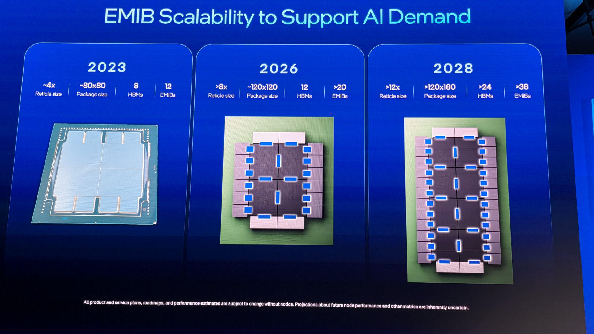
Intel's EMIB has evolved dramatically since entering high-volume manufacturing in 2017. What started as a relatively straightforward way to connect adjacent chiplets without using an expensive silicon interposer has become a sophisticated packaging technology used for data center processors and is set to enable massive AI accelerators 12 times the size of a reticle with dozens of silicon bridges, more than 24 HBM stacks, and advanced power delivery.
(Image credit: Tom's Hardware)
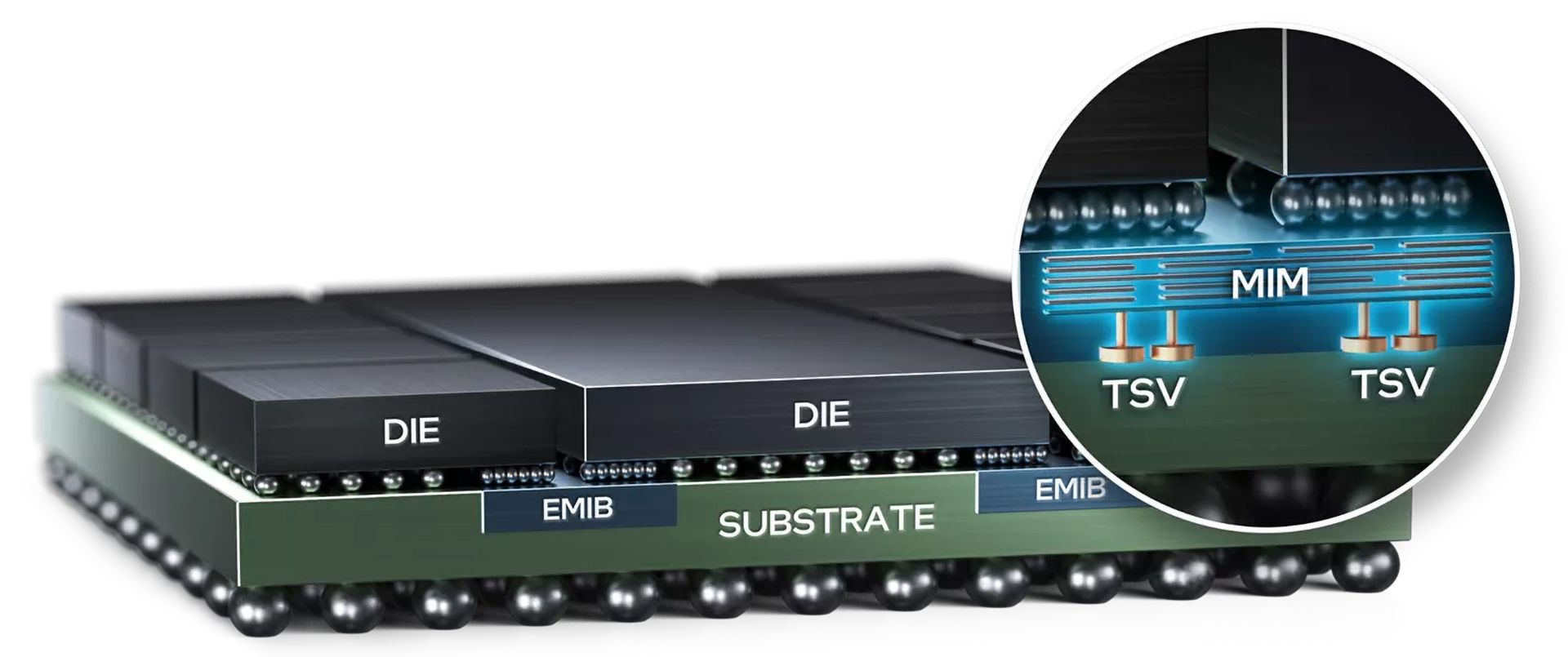
The basic idea behind EMIB remains unchanged almost a decade after its first introduction. Instead of placing compute and memory dies on a large silicon interposer, Intel embeds tiny silicon bridges into an organic package substrate only where high-density die-to-die connectivity is required (try to find those bridges!). This reduces silicon usage and allows the rest of the package to use conventional substrate wiring and relaxed bump pitches. Early EMIB implementations used a 55-µm first-layer-interconnect (FLI) bump pitch, which Intel subsequently reduced to 45 µm. Intel's recent roadmaps indicate further reductions to around 36 µm and ultimately 25 µm, which dramatically increases the number of connections that can fit along a chiplet's edge (shoreline density).
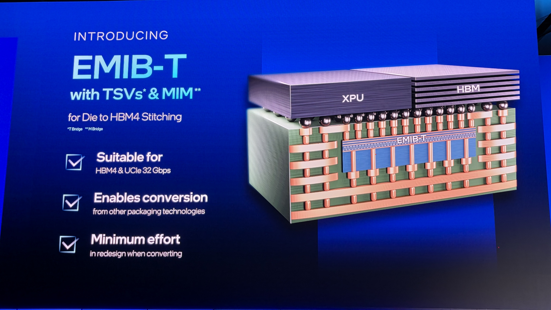
In addition to shrinking FLI bump pitches and increasing connection density, Intel is also adding functionality to the bridges themselves. EMIB-M incorporates metal-insulator-metal (MIM) capacitors into the bridge to improve power delivery and suppress voltage fluctuations close to compute dies. The newer EMIB-T takes this concept considerably further by adding through-silicon vias (TSVs), which enable power to travel vertically through the bridge instead of taking longer paths around it. This becomes increasingly important for multi-kilowatt system-in-packages (SiPs) and HBM4-class memory subsystems, where both current density and power integrity are major packaging constraints.
EMIB roadmap
EMIB 1st Gen
EMIB 2nd Gen
EMIB-M
EMIB-T
EMIB-T evo
EMIB-T glass
Bump Pitch
55 µm
45 µm
45 µm ~ 36 µm
45 µm ~ 36 µm
25 µm
Number of Bridges
6
12
>20
>38
?
?
Bump Density
330 mm^2
494 mm^2
494 => 772 mm^2
494 => 772 mm^2
1600 mm^2
1600 mm^2
C2C Power
0.5 pJ/bit
0.3 - 0.5 pJ/bit
0.25 pJ/bit
0.25 pJ/bit
?
?
TSV
-
-
-
+
+
+
Die Complex
2X reticles
4X reticles
8X reticles
12X reticles
?
panel
HBM Stacks
4
8
12
24
?
?
Capacitor
-
-
MIM
MIM
MIM (?)
MIM (?)
Substrate
organic
organic
organic
organic
organic
glass
Package size (mm)
50 × 50
80 × 80
120 × 120
120 × 180
?
240 × 240 (?)
Year
2017 - 2023
2023
2024 - 2026
2028
?
2030+
Such SiPs are not only complex, but they are physically large, so Intel's EMIB has evolved to support larger designs. Firstly, a finer FLI pitch increases the interconnect density required to build bigger SiPs. Secondly, EMIB-M addresses the power-integrity problem created by big processors, such as Intel's Xeon 6 'Granite Rapids.' Thirdly, EMIB-T simplifies power routing, lowers impedance, and reduces noise, which will get more important when faster versions of UCIe (32 GT/s and higher) become commonplace. Intel's consistent EMIB technology development has enabled the company to move from an SiP of 4X reticle size on an 80×80 mm package earlier this decade, to something closer to 8X reticles on a 120×120 mm package today, and even larger 12X SiPs on a 120×180 mm package in the future.
Eventually, Intel plans to combine finer-pitch EMIB technology with glass-core substrates. Glass offers better stability and reduced warpage compared with organic materials, which becomes increasingly important as packages grow to enormous sizes. Glass will likely be one of EMIB's biggest advancements, as it will enable improvements in multiple directions, including performance and dimensions.
(Image credit: Tom's Hardware)
Intel says EMIB-T is on track for mass production in 2027 and its yields and reliability are meeting its targets. If those ramps proceed as planned, EMIB will have evolved from an alternative to a silicon interposer into one of Intel Foundry's key technologies for building massive AI systems.
"Customer interest in EMIB-T continues to be very high – the technology is compelling, providing capabilities for advanced AI silicon solutions which are not possible with today's mainstream offerings," said Lip Bu Tan, chief executive of Intel, in an August 2026 earnings call. "We continue to have a growing EMIB-T backlog, yield and reliability are hitting targets, and we are focused on ramping the technology into high volume and high quality to support customer ramps in 2027."
EMIB-T with MIM (Image credit: Intel)
Intel is scaling EMIB along several directions simultaneously: finer interconnect pitch, more bridges, larger substrates, denser power delivery, faster memory interfaces, and dramatically larger SiPs. Intel formally positions EMIB as a cost-effective advanced packaging technology that uses local silicon bridges for logic-to-logic and logic-to-HBM connections in an organic substrate instead of large silicon interposers used by solutions like TSMC's CoWoS-S. Meanwhile, there are applications that can benefit from large, rigid interposers or flexible organic redistribution layer interposers. To address these applications, Intel's Foveros portfolio includes Foveros-S, Foveros-R, and Foveros-B, which more directly mirror TSMC's CoWoS-S, CoWoS-R, and CoWoS-L packaging technologies, respectively.
Foveros 2.5D: A fistful of packages
Intel's Foveros packaging technology is evolving from its original chip-on-wafer implementation that emerged in 2019 with the Lakefield processor into a broad family of 2.5D and 3D integration technologies designed to address everything from cost-sensitive client processors to large HPC and AI systems.
(Image credit: Tom's Hardware)
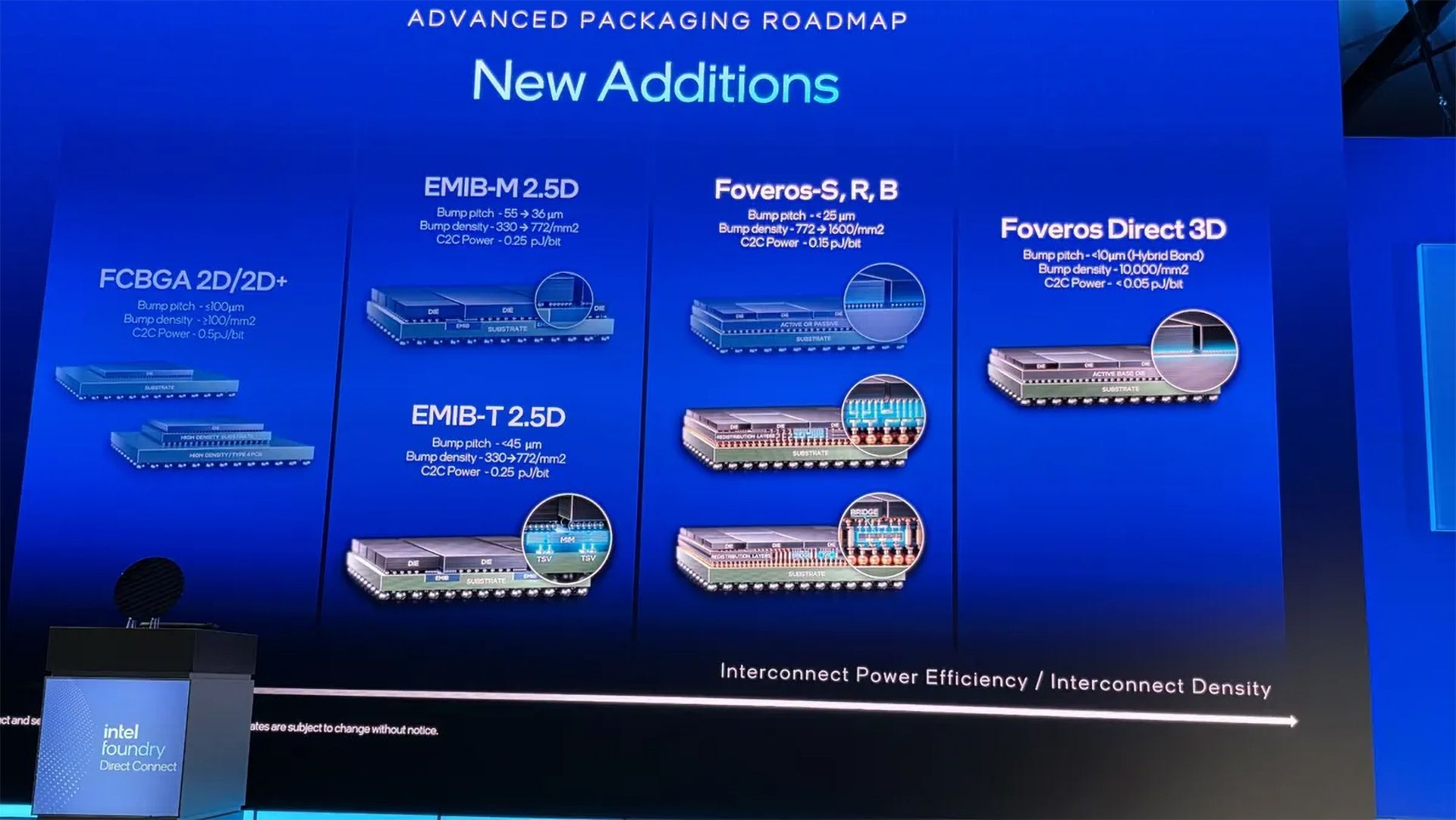
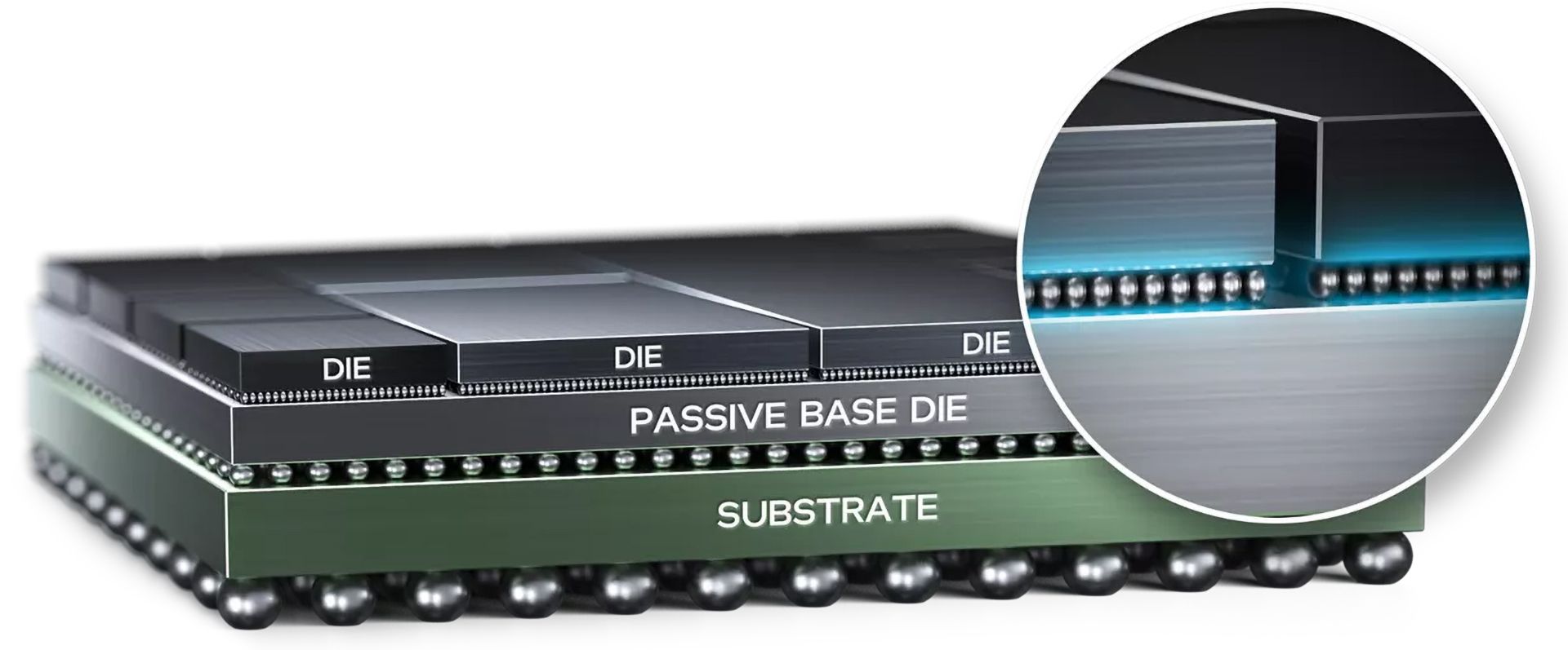
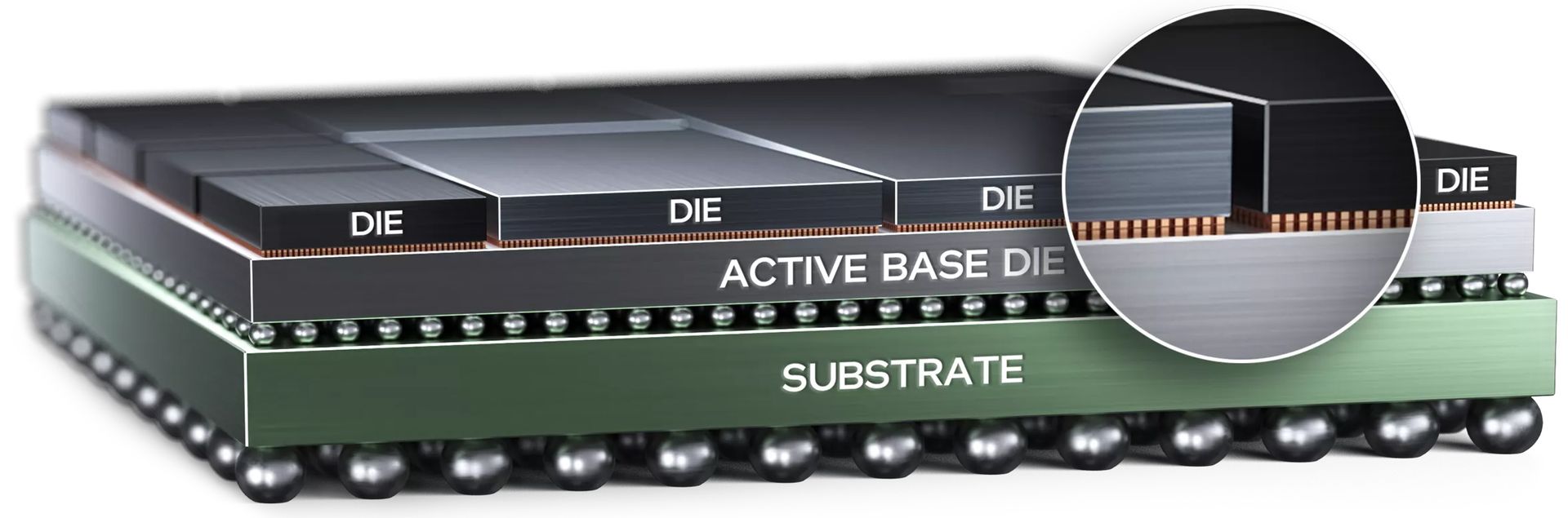
The original Foveros technology used an active 22FFL-based silicon base die, or interposer, with through-silicon vias (TSVs) and active dies attached using face-to-face bonding. Intel's Lakefield and Ponte Vecchio used active base dies and 36 µm microbump pitches, whereas Meteor Lake, Arrow Lake, and Panther Lake implementations use a passive base with a 36 µm microbump pitch. Since the introduction of Foveros with active and passive base dies in 2019 – 2023, Intel has also diversified Foveros to address different cost and integration requirements. The latest Foveros 2.5D roadmap — which mentions -S, -R, and -B variants with similar characteristics — presented in mid-2025, takes Foveros considerably further from its original capabilities: it targets pitches below 25 µm, bump density increase from 772 to 1,600 connections per mm², and chip-to-chip interconnect power of 0.15 pJ/bit.
Foveros roadmap
Foveros-S
Foveros-R
Foveros-B
Bump Pitch
36µm => 25µm =>
36µm => 25µm =>
36µm => 25µm =>
Hybrid Bonding
-
-
-
Local Bridges
-
-
Yes
Bump Density
772-> 1600/mm^2
772-> 1600/mm^2
772-> 1600/mm^2
C2C Power
0.15 pJ/bit
0.15 pJ/bit
0.15 pJ/bit
TSV
-
-
?
Die Complex
4X reticle
RDL limited
Bridge limited
HBM Stacks
8 (?)
Dependant upon interposer size
Dependant upon interposer size
Capacitor
-
?
Substrate
Organic
Organic
Organic
Package size (mm)
?
?
?
Year
2019
2027
?
For now, the most advanced and yet production-proven Foveros 2.5D technology is Foveros-S. This packaging technology places multiple chiplets on a silicon interposer and currently supports packages up to four reticles in size, which is below what TSMC offers with CoWoS-S (up to 5.5X reticles). Since Foveros-S is essentially an evolution of the original Foveros from 2019, Intel legitimately says that it has been in volume production since 2019. Yet, going forward, Foveros-S will be evolving in multiple directions, which includes larger package sizes, interconnect density, and interconnect power efficiency.
Foveros-S (Image credit: Intel)
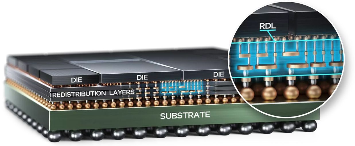
Foveros-R removes the silicon interposer altogether and uses fan-out RDL technology to optimize cost and interconnect density. Intel says the implementation can use up to three redistribution layers. The method is designed to offer a balance between cost and interconnect density and enable heterogeneous integration of chiplets from different sources through UCIe. Like the other members of Intel's current Foveros 2.5D family, the technology uses 36 µm microbump pitches, but is designed to support pitches below 25 µm as well as bump density scaling from 772 to 1,600/mm² and chip-to-chip interconnect power of 0.15 pJ/bit. Intel says Foveros-R will be production-ready in 2027.
Foveros-R (Image credit: Intel)
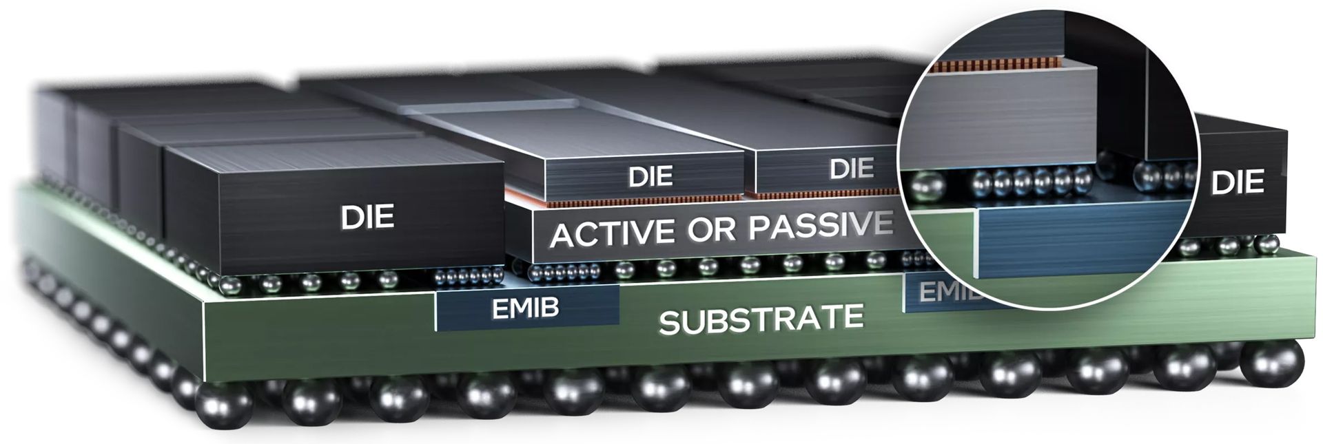
Foveros-B extends the concept toward larger and more complex AI/HPC designs. Instead of relying on a full silicon interposer, the technology combines RDLs with local active or passive silicon bridges that provide high-density connections only where they are needed. This potentially gives Intel an intermediate option between an RDL-only implementation and a large silicon interposer, as well as a direct competitor for TSMC's CoWoS-R.
Note that Intel does not explicitly say that Foveros-B uses EMIB bridges, though given similar microbump pitch sizes and the plan to use active local bridges in the future, Foveros-B's bridges are likely to closely resemble EMIB-M and EMIB-T bridges. If Foveros-B can indeed use EMIB bridges, future Foveros-B designs could also incorporate cache disaggregation, integrated voltage regulators (IVRs), or MIM capacitors.
As for interconnection densities and power, Foveros-B is listed as designed to support pitches below 25 µm, bump density scaling up to 1,600/mm², and chip-to-chip interconnect power of 0.15 pJ/bit. Meanwhile, Intel has not disclosed when Foveros-B will be ready for commercial production, so its actual specifications remain to be seen.
With EMIB and the Foveros 2.5D portfolio, Intel can address a broad range of applications, but Intel's scaling is not stopping. In addition to 2.5D lateral scaling enabled by EMIB or Foveros 2.5D, it can stack chiplets on top of each other using its Foveros 3D and EMIB 3.5D packaging technologies.
Foveros Direct 3D: There will be copper (and no bumps)
Unlike simple package-on-package stacking, which has existed for decades, densely interconnected 3D stacking essentially turns separate dies into parts of the same tightly coupled chip, increasing bandwidth, reducing latency, cutting interconnect power, and shrinking footprint. The challenge is manufacturing thousands of extremely fine connections between dies while maintaining yield, power delivery, signal integrity, and — perhaps most importantly — removing heat from chips buried inside the stack.
Foveros Direct 3D (Image credit: Intel)
The biggest architectural step in Intel's Foveros roadmap is Foveros Direct 3D, which moves from microbump-based connections toward direct copper-to-copper hybrid bonding. Conventional microbumps cannot shrink forever, as solder bumps need sufficient dimensions to maintain manufacturing yield and reliability, while the solder itself introduces additional resistance and parasitic effects. Foveros Direct 3D eliminates solder altogether and directly bonds copper pads on one die to those on another, which enables an interconnect pitch below 10 µm — up to 10 times finer than conventional microbump technology.
Foveros Direct 3D 1st Gen
Foveros Direct 3D 2nd Gen
Joint
Cu–Cu hybrid bond (no solder)
Cu–Cu hybrid bond (no solder)
Pitch
9 µm (public “sub-10 µm”)
3 µm
Pad Density
~12,300/mm^2 (Intel: >10,000)
Over 100,000/mm^2
C2C Power
Not published (same class or lower)
Base die
Active
Active
TSV
+ (in base; 18A-PT adds pass-through TSV)
+
Capacitor/Extras in Base
MIM; Clearwater Fores adds LLC + IVR
MIM; Clearwater Fores adds LLC + IVR
HBM Stacks
No direct limit — attached via EMIB 3.5D
No direct limit — attached via EMIB 3.5D
Die Complex
Set by EMIB 3.5D when used together
Set by EMIB 3.5D when used together
Substrate
Organic (glass later if EMIB-T glass)
Organic (glass later if EMIB-T glass)
Package Size
Follows EMIB 3.5D (~80×80 → 120×180)
Follows EMIB 3.5D (~80×80 → 120×180)
Year
2026
Later
Intel claims that Foveros Direct 3D can offer bonding pitch of sub-10 µm, interconnect density of up to 10,000 connections per mm², and chip-to-chip interconnect power below 0.05 pJ/bit. Such dense connectivity shortens signal paths between stacked dies, increases bandwidth, reduces latency, and cuts the energy required to move data. In addition to electrical advantages, direct bonding creates more continuous thermal paths between dies, which Intel says improves heat dissipation compared with conventional packaging, which is crucially important as vertically stacked logic pushes power density dramatically higher.
Intel's Foveros Direct 3D bonding interface supports both face-to-back and face-to-face stacking. In addition, Intel has described chip-to-wafer as well as wafer-to-wafer bonding.
As Intel's schematic drawing of a Foveros Direct 3D-based system-in-package shows (and Intel confirms), the technology is much more flexible than simply placing one logic die on top of another. The method can support different die sizes, multiple stacking levels, and can combine dies manufactured using different process technologies in one SiP.
Intel's Xeon 6+ 'Clearwater Forest' processor is the first product to use Foveros Direct 3D copper bonding in volume to attach Intel 18A compute chiplets to active base dies. The CPU uses the 1st Generation Foveros Direct 3D with 9 µm copper bonding pitch. Meanwhile, Intel plans to shrink bonding pitch to 3 µm with its 2nd Gen Foveros Direct 3D. To put these numbers into perspective, TSMC's 1st Gen SoIC from 2023 supports pitches of 9 µm (AMD's 2nd Gen 3D V-Cache uses this version), whereas the latest generation that entered volume production in 2025 features bonding pitches of 6 µm. TSMC expects to shrink SoIC's interconnection pitch to 4.5 µm by 2029.
EMIB 3.5D: Everything everywhere all at once
Finally, Foveros and EMIB do not have to operate independently. Intel can combine Foveros 2.5D or Foveros Direct 3D with substrate-embedded EMIB bridges to create what it calls EMIB 3.5D in a bid to build its ultimate products. In this architecture, Foveros provides dense local 2.5D or 3D connectivity within individual chiplet assemblies, while EMIB provides high-bandwidth horizontal connections between these modules, essentially building a massive system-in-package out of smaller SiPs. Intel says the individual SiPs can be identical to scale performance, or distinctive, to enable different functionality.
EMIB 3.5D (Image credit: Intel)
The combination of EMIB and Foveros is particularly useful because it enables Intel to scale both horizontally and vertically without placing the entire system on one massive silicon interposer. Intel says EMIB 3.5D can achieve a total silicon surface area considerably larger than what its existing silicon-interposer-based technologies can accommodate. Intel first used EMIB 3.5D to build its Ponte Vecchio compute GPU that integrated 47 active tiles manufactured on five process nodes and contained more than 100 billion transistors. Although Intel's Data Center GPU Max can hardly be called a smashing success, it certainly demonstrated what Intel can do with its advanced packaging technologies.
EMIB 3.5D roadmap
EMIB 3.5D (Foveros)
EMIB 3.5D (Direct 1st Gen)
EMIB 3.5D (Direct 2nd Gen + EMIB-T)
Vertical Joint
solder microbump
Cu–Cu hybrid
Cu–Cu hybrid
Vertical Pitch
36 µm
9 µm
3 µm
Vertical Density
828 /mm² (Intel)
>10,000 /mm² (Intel)
Not published
Energy
~0.15 pJ/bit
Not published
Lateral Joint
EMIB 1st gen
EMIB 2nd gen
EMIB-T
Lateral Pitch
55 µm
45 µm
45 → 36 → 25 µm
Lateral Energy
~0.5 pJ/bit
0.25 pJ/bit
0.25 pJ/bit
Base Die
Active
Active
Active
TSV
Foveros base
Foveros base
Base + EMIB-T
HBM
via EMIB (PVC: 8)
Optional (CWF: DDR)
via EMIB-T (12 → >24)
Bridges (example)
11 (PVC)
12 (CWF)
>20 → >38
Package
~80 × 80 mm
Xeon module
120 × 120 → 120 × 180 mm
Product
Ponte Vecchio
Clearwater Forest
TBC
Year
2022
2026
Later
Going forward, the EMIB 3.5D architecture becomes considerably more promising when combined with Foveros Direct 3D. Using both will enable Intel to build tightly coupled compute modules using ultra-dense vertical copper-to-copper connections, and then link multiple modules laterally using EMIB, essentially scaling complex processors both vertically and horizontally. However, surprisingly, Intel decided not to use EMIB 3.5D for its next-generation Xeon 'Diamond Rapids' processor: while the CPU uses Foveros Direct 3D for vertical integration, UCIe-S connections are used for lateral interconnects.
Multi-die another day
While Intel's EMIB and Foveros technologies emerged to serve different kinds of scaling, the company is evolving them into a complementary platform that can scale complex processors both horizontally and vertically.
(Image credit: Intel)
EMIB is progressing toward finer interconnect pitches, vertical power delivery, glass substrates, and packages exceeding 12 reticles with more than 24 HBM stacks, while the expanding Foveros family spans from 2.5D integration all the way to ultra-dense Foveros Direct 3D hybrid bonding. In fact, Foveros Direct 3D already enables sub-10-µm copper-to-copper connections and is headed toward even finer pitches.
Meanwhile, EMIB 3.5D combines vertically stacked modules with lateral EMIB links to create large heterogeneous system-in-packages for ultimate AI and HPC applications without using enormous silicon interposers.
What is perhaps interesting to note is that, for now, Intel lacks a system-on-wafer platform to enable Cerebras WSE and Tesla Dojo-like wafer-scale processors, though this is explainable, as demand for such technologies is too limited today and may not pick up significantly tomorrow.
Elon Musk's Terafab will get its first EUV lithography tool in the middle of next year, reports Tim Culpan, citing sources with knowledge of the matter. But considering that the shell of the firm's development fab will not be completed until late 2027 and that tools will only begin to be moved in later that year, according to SemiAnalysis, the scanner will sit idle for some time.
Tesla broke ground on its research fab on the north campus of Giga Texas near Austin this past April. SemiAnalysis expects the building to be completed in 15 months and predicts it will take Tesla a further six months to install equipment and production tools, after which it will be able to start processing wafers, or rather experimenting with chip production to get the team prepared for completion of the Terafab volume fab phase 1.
Given how hard it is to get an ASML Twinscan NXE EUV lithography tool these days, storing it for several months before putting it to use may sound like an expensive slack period, but it's not the significant financial problem for Terafab that it would be for a traditional chipmaker.
The projected delivery of a conventional EUV lithography system to Terafab also indicates that while Elon Musk has praised free electron laser (FEL) light sources for lithography tools, the first-generation efforts of his semiconductor production company will rely on more traditional equipment. This is not particularly surprising, as Terafab is set to use Intel's 14A manufacturing technology. 14A will use not only existing Low-NA EUV scanners, but also next-generation High-NA EUV machines.
Using lithography systems with unconventional and largely untested light sources would require substantial modifications to the manufacturing process, extensive equipment qualification, and potentially changes to photomasks and photoresists, which would complicate the transfer of Intel’s 14A technology and delay Terafab's production ramp.
But usage of standard lithography equipment does not mean that Musk's company has no plans to use tools that are different from those used by Intel, though for now it is too early to make guesses about what Terafab engineers might change in terms of fab configuration.
SpaceX announced that it had selected Grimes County for Terafab in early August 2026. By now, there is evidence that work has progressed beyond clearing land, as drone footage published by Joe Tegtmeyer in mid-September showed foundation excavation and rebar cage installation at the northwestern part of the site. This suggests that contractors had begun structural construction by early September, although the precise purpose of the foundation is unknown.
Right now, SemiAnalysis reports that project Terafab Grimes phase 1 will be built in 20 months, equipped in 17 months, and ramped to volume in six months. Analysts project that the fab will begin operation in late 2029 and then ramped to volume by mid-2030.
An interesting note about Terafab's volume fab is that SpaceX reportedly ordered semiconductor manufacturing equipment in April 2026, several months before officially announcing the Grimes County location. This indicates that the company committed to its manufacturing plans well before the public groundbreaking. In addition, this makes the mid-2028 equipment installation forecast plausible, given the long lead times associated with advanced semiconductor manufacturing equipment.
Intel plans to begin risk production using its 14A (1.4nm-class) fabrication process in the second half of 2027 and initiate high-volume manufacturing (HVM) in the second half of 2028 if everything goes as planned. This puts Intel's ramp into HVM at least 1.5 years ahead of SpaceX’s Terafab Grimes Phase 1.
This means that while Terafab will get a proven advanced manufacturing technology, presumably with decent yields, it will not be the absolute best production node at the time, as TSMC intends to start volume production of chips using its A12 fabrication process in late 2029. A12 is a 1.2nm-class process with TSMC's second-generation nanosheet GAA transistors and backside power delivery. Intel will be close to unveiling its 14A-P node at the same time.
Nonetheless, since Terafab will likely exclusively serve SpaceX, Tesla, and xAI, a slightly less advanced node will not be a big problem for the company, as the potential cost increases incurred by using a more sophisticated manufacturing technology will be offset by using an in-house production facility.
Following its win against Arm in its licensing dispute around CPU cores developed by Nuvia, Qualcomm sued Arm in the U.S. early this year, accusing its partner of breaching the terms of their contract and causing damages to the company. This week a federal jury in Delaware has ruled that Arm indeed breached its contractual obligations with Qualcomm and intentionally interfered with the chipmaker's business relationship with Meta. However, the jury awarded Qualcomm only $2 in nominal damages and rejected several other claims against Arm. As a result, both companies declared victory in the latest round of their legal dispute, which could still have massive financial consequences.
The verdict followed a five-day trial in Wilmington, Delaware, during which Qualcomm accused Arm of violating the Architecture License Agreement (ALA), withholding software patches and processor verification tools, and refusing to offer commercially reasonable licensing terms. In particular, Qualcomm alleged that Arm deliberately withheld Arm Compliance Kit (ACK) verification materials and software patches necessary to validate its custom CPUs. Qualcomm also claimed that Arm refused to renew licenses for Cortex-A720, Cortex-A520, and Cortex-M55 processor cores under its Technology License Agreement (TLA).
Qualcomm further alleged that Arm deliberately undermined its relationships with customers by threatening to terminate its architecture license and leaking the corresponding notice to the media in October 2024. The company said that Arm's actions disrupted its negotiations with Meta and other customers, which caused financial losses as the company failed to land contracts with certain clients. Arm denied any wrongdoing and argued that Qualcomm had failed to demonstrate substantial financial losses. The company also indicated that Qualcomm intended to use the litigation to obtain more favorable licensing terms and avoid billions of dollars in royalty payments.
The jury sided with Qualcomm on two issues. First, it determined that Arm had breached its longstanding ALA, which allows Qualcomm to develop and sell custom processors compatible with Arm's instruction set architecture. Second, it found that Arm had intentionally interfered with Qualcomm's business relationship with Meta. Qualcomm welcomed the verdict and maintained that it exposed Arm's efforts to undermine its business and eventually become a Meta supplier.
"We are gratified that the jury found Arm breached its long-standing Architectural License Agreement (ALA) with Qualcomm, failed to honor its commitments, and intentionally acted to disrupt Qualcomm's businesses," a statement by Qualcomm reads. "Together with Qualcomm's prior court victory, this outcome further exposes Arm’s broader intentions to harm Qualcomm and its ecosystem. This outcome is a victory for innovation and competition, and we remain focused on developing and delivering industry-leading semiconductor products including our Oryon CPUs to customers and consumers worldwide."
However, Arm prevailed on four of Qualcomm's six claims submitted to the jury and was ordered to pay just $1 in damages on each of the aforementioned two. The original complaint included allegations of breaches of the ALA and TLA, violations of the implied covenant of good faith and fair dealing, intentional and negligent interference with prospective economic advantage, and unfair competition. The precise findings on the individual allegations have yet to be revealed, as at press time the jury rulings were not available. Arm claims that the outcome supports its position that it had acted in good faith under its technology license agreement.
"We are pleased with the jury’s decision today finding for Arm on four claims and awarding only one dollar in damages on each of Qualcomm’s other two claims," a spokesperson for Arm said. "Despite Qualcomm's pursuit of this case in an attempt to deprive Arm of billions of dollars under our license agreements, the jury's verdict confirms that Arm operated in good faith under its technology license agreement and its award of only two dollars confirms the merit of Arm’s arguments in the case."
Qualcomm’s complaint
Details of the allegation
Outcome
I
Breach of the Architecture License Agreement (ALA)
Arm allegedly violated provisions of Qualcomm’s ALA, including its obligations concerning the agreement’s validity and Qualcomm’s licensing rights.
Not separately confirmed
II
Breach of the ALA — failure to deliver technical resources
Arm allegedly withheld Arm Compliance Kit (ACK) verification materials, out-of-band (OOB) test lists, and software patches needed to validate Qualcomm’s custom processors.
Qualcomm prevailed on an ALA breach claim, but the exact count requires confirmation.
III
Breach of the implied covenant of good faith and fair dealing
Arm allegedly acted in bad faith by withholding technical resources, threatening license termination, interfering with customers, and refusing to negotiate future licensing terms.
Exact disposition unconfirmed. A related good-faith negotiation issue was considered separately by the judge.
IV
Intentional interference with prospective economic advantage
Arm allegedly deliberately disrupted Qualcomm’s relationships with customers, including Meta, through its license-termination threats and communications.
Qualcomm prevailed on intentional interference concerning Meta.
V
Negligent interference with prospective economic advantage
Arm allegedly failed to exercise reasonable care when its actions disrupted Qualcomm’s existing and prospective customer relationships.
Not separately confirmed
VI
Violation of California’s Unfair Competition Law
Arm allegedly engaged in unfair business practices intended to prevent Qualcomm from competing with Arm’s processor designs.
Not separately confirmed
VII
Breach of the Technology License Agreement (TLA)
Arm allegedly failed to offer commercially reasonable licensing terms for processor IP, including Cortex-A720, Cortex-A520, and Cortex-M55.
Arm prevailed on TLA-related claims, but the exact count requires confirmation.
VIII
Breach of another TLA provision
Arm allegedly violated additional contractual protections concerning the terms offered for processor IP.
Arm prevailed on TLA-related claims, but the exact count requires confirmation.
Despite the nominal $2 damages award, the legal battle between Qualcomm and Arm is not over. U.S. District Judge Maryellen Noreika must still determine whether Arm's breach of its Architecture License Agreement entitles Qualcomm to suspend royalty payments for five years, potentially costing Arm hundreds of millions, or even billions, in revenue. The judge must also decide whether Arm violated its obligation to negotiate future architecture licensing terms in good faith. Both decisions could have substantially greater financial and commercial consequences than the jury's verdict, and either company could appeal an unfavorable ruling.
When GlobalFoundries abandoned development of leading-edge nodes in 2018, it also canceled the development of its 7nm-class FinFET fabrication technology that it co-developed with IBM. Almost exactly eight years later, GlobalFoundries is back with a 7nm-class manufacturing process, only this time the node relies on planar transistors and fully-depleted silicon-on-insulator (FD-SOI). It is aimed at automotive, edge AI, industrial, robotics, sensors, and other devices that prioritize low power consumption, high integration, and cost efficiency over maximum performance.
"We are delighted that GlobalFoundries has announced its next-generation 'single-digit FD-SOI; node, building on technology that CEA-Leti has been advancing for decades," said Sébastien Dauvé, chief executive of CEA Leti. "Through the FAMES pilot line, CEA-Leti continues to shape the future European roadmap for FD-SOI and works every day to promote its adoption in a wide range of applications."
FDX Fusion enters the scene
The new fabrication technology from GlobalFoundries is called FDX Fusion, and it promises 7nm-class 'digital performance' (an ambiguous claim; we will try to interpret it later) and more than twice the transistor density of its original 22FDX process introduced circa 2015. To achieve its target goals, the first generation of FDX Fusion will combine innovations in SOI substrates, transistor structures, and back-end interconnects, though keep in mind that GF has not disclosed transistor dimensions, contacted gate pitch, minimum metal pitch, or actual transistor density. GF plans to launch production of chips on FDX Fusion at its Dresden, Germany, facility in 2028, which will mark its return to the development of substantially more advanced FD-SOI fabrication processes after years of efforts to enhance its existing 22nm-class platform.
In addition to improved 'digital performance,' FDX Fusion will support RF transistors with fT/fmax of up to 0.5 THz, analog and mixed-signal circuitry, embedded nonvolatile memory, and in-memory computing capabilities. The combination is intended to enable highly integrated chips that can process information from sensors, execute AI inference workloads, control external devices, and communicate wirelessly without the need for numerous separate ICs. GF also intends to provide processor IP based on MIPS, ARC, and RISC-V architectures to accelerate the development of such products.
That being said, the main selling point of FDX Fusion is not necessarily its 7nm-class 'digital performance' and high-performance processor IP, but rather its ability to combine relatively powerful digital logic with RF, analog and mixed-signal circuitry, embedded nonvolatile memory, and in-memory computing capabilities on a single chip. This combination — which is why GloFo calls the process technology FDX Fusion — could enable highly integrated SoCs that would otherwise require multiple chips manufactured on different process technologies, which means additional tapeout costs as well as power consumption.
GlobalFoundries said it plans to deliver initial demo silicon for customer evaluation in early 2027, followed by the first process design kit (PDK) in mid-2027. The company is already collaborating with several customers on the technology, although it has not identified specific products or committed production volumes. Specifically, GF mentioned in its press release that BMW, Bosch, Infineon, NXP, Siemens, and Tesla have expressed interest in FDX Fusion, though only Infineon specifically confirmed collaboration on future 7nm-class technologies for radar and wireless communications.
Significant development
The GlobalFoundries announcement represents a significant development for GF's FD-SOI roadmap. The company introduced 22FDX in 2015 and announced its 12FDX successor in 2016, which promised performance comparable to 10nm FinFET, full-node density improvements, and up to 50% lower power consumption. Initial 12FDX customer tape-outs were expected in 2019, but the technology has never been adopted for commercial products. Instead, GF focused on enhancements to 22FDX and eventually the introduction of 22FDX+ (around the time when Samsung unveiled its 18FDS+), with additional capabilities for RF, embedded memory, and low-power applications. Interestingly, 12FDX was still a part of GF's investor roadmap in 2022.
FDX Fusion could therefore represent the realization of GF's original ambitions to scale FD-SOI beyond 22nm-class, although the company has not explained whether the new technology incorporates developments from its earlier 12FDX program. Meanwhile, CEA-Leti, which has conducted research into advanced FD-SOI technologies for years, describes FDX Fusion as a single-digit FD-SOI node. Nonetheless, GF's claim of 7nm-class 'digital performance' does not necessarily imply comparable transistor dimensions or integration density.
From an industry perspective, FDX Fusion could provide an alternative to advanced FinFET and perhaps even gate-all-around processes for applications that require reasonably powerful digital logic alongside RF, analog, and embedded memory. Such integration could reduce system complexity and power consumption, particularly in edge AI devices where energy efficiency and real-time responsiveness are critical.
Perhaps more importantly, the technology could give European semiconductor developers access to a more advanced locally manufactured process without dependence on leading-edge foundries in Asia or the U.S.
Questions remain
However, the commercial success of FDX Fusion will depend on its actual performance, density, production costs, and the availability of a competitive design ecosystem, the latter arguably being the hardest part given the lack of any comments from leading electronic design automation (EDA) and IP developers.
When GlobalFoundries claims 2X 'digital performance' comparable to that of 7nm-class technologies, it doesn't reveal whether it means transistor switching speed, standard cell performance, achievable operating frequency, or something else. In addition, the company promises more than twice the logic density of its first-generation FDX technology, although the firm does not reveal any actual numbers. Consequently, it is unclear how FDX Fusion will compare with established 7nm-class FinFET technologies, which offer mature defect density and yields, plenty of supply, an established design ecosystem, and predictable pricing among other things, in terms of transistor density, performance, power consumption, and production costs. While CEA-Leti's comment seems promising, actual numbers are always better.
The very fact that GF's FDX Fusion planned 2028 introduction will come roughly nine years after the originally anticipated first 12FDX tape-outs illustrates significant technological and/or financial difficulties associated with the development of FD-SOI beyond the 22nm generation. So, while GlobalFoundries' FDX Fusion initiative certainly looks promising, it remains to be seen how that is going to play out for the contract chipmaker and its clients.
For now, the lineup of supporters from the automotive and industrial sectors — BMW, Bosch, Infineon, NXP, Siemens, and Tesla — certainly looks promising. But what about other applications? While established semiconductor companies such as Infineon and NXP already possess extensive processor IP portfolios, smaller fabless developers could benefit from GF’s MIPS and ARC processor cores, RISC-V expertise, and custom chip design capabilities, which could substantially reduce the cost and complexity of developing specialized SoCs. Still, to attract a broader range of chip developers, GlobalFoundries will need a mature ecosystem of EDA tools, standard-cell libraries, memory compilers, interface IP, and other silicon-proven building blocks. These are the things that GlobalFoundries has not touched upon in its press release.
Just five years after bringing its Software Guard Extensions (SGX) technology to its mainstream server platform, Intel on Friday announced plans to discontinue its support after its upcoming Xeon 'Diamond Rapids' CPUs and concentrate its confidential computing efforts on Trust Domain Extensions (TDX). The company will continue to support existing SGX-enabled platforms into the early 2030s, but at the same time will expand TDX capabilities to address emerging requirements of cloud computing, enterprise workloads, and agentic AI applications.
Without a doubt, data sovereignty requirements are an increasingly important factor as organizations seek to protect sensitive information from unauthorized access even when they process it on infrastructure operated by third parties. Although both Intel SGX and TDX are designed to protect sensitive information while it is being processed, they use substantially different approaches.
SGX provides hardware-protected enclaves within applications to isolate selected code and data from other software, including the operating system and hypervisor. By contrast, TDX isolates entire virtual machines from the underlying host environment, including the hypervisor and other VMs. While SGX requires developers to design or modify applications to use protected enclaves, TDX can protect existing workloads inside confidential VMs without extensive changes to individual applications, something that makes TDX particularly attractive to cloud service providers that operate large numbers of virtual machines.
While both SGX and TDX have faced numerous security vulnerabilities over the years, including side-channel attacks, privilege-escalation flaws, and attacks against their attestation mechanisms, Intel does not cite security concerns as a reason for its decision to discontinue SGX.
Intel's decision to phase out SGX reflects the industry's preference for VM-level isolation over application-specific enclaves. According to Intel, TDX provides scalability, ease of deployment, and the operational model required for widespread adoption of confidential computing. Although SGX enabled confidential computing in the data center and continues to serve security-conscious customers, Intel believes future demand will favor TDX. Diamond Rapids will therefore be the final Xeon generation to support SGX, which gives customers several years to validate alternative solutions based on TDX and migrate existing applications. Intel will continue to provide security updates and support for SGX-enabled platforms into the early 2030s, so its customers will have plenty of time to adopt TDX for new deployments.
Meanwhile, Intel plans to expand TDX capabilities with additional security technologies. These include Intel TDX Connect, which is designed to enable trusted I/O, as well as post-quantum cryptography and enhanced attestation mechanisms. Trusted I/O is particularly important for workloads that communicate with external devices, as protection of computations inside a virtual machine does not necessarily extend to data transferred between the VM and accelerators or other peripherals (read, CXL expanders, though Intel has not stated this for sure). Improved attestation will help organizations verify the integrity of protected environments, while post-quantum cryptography will help address future security threats. Meanwhile, Intel has not disclosed specific availability dates for these enhancements.
One important driver behind Intel's confidential computing strategy seems to be accelerated adoption of agentic AI. Unlike conventional applications, autonomous agents may access sensitive enterprise information, execute operations across multiple systems, and interact with other agents. Intel expects many such workloads to run on CPUs, and here TDX may offer practical advantages for agentic AI applications. Unlike SGX, TDX can protect entire agent execution environments without extensive software modifications and enable multiple agents to operate in separate, hardware-isolated VMs on shared infrastructure. For GPU-accelerated AI workloads, Intel works with Nvidia to coordinate confidential computing technologies across CPUs and GPUs to extend protection to sensitive data and AI models throughout the processing pipeline (which is obviously broader than Intel's development of custom Xeon CPUs for Nvidia).
Intel TDX is already available through major cloud providers, including Alibaba Cloud, Google Cloud, IBM Cloud, Microsoft Azure, and Volcano Cloud. Meanwhile, Red Hat, Canonical, and VMware are adding TDX support to their software platforms to enable adoption in private clouds and enterprise environments.
Frore Systems has introduced its bespoke LiquidJet Diamond liquid-cooling coldplate series that uses a diamond surface combined with a multi-stage 3D short-loop jet-channel microstructure to address precise hotspots on next-generation AI accelerators, such as AMD's Instinct MI400 and MI500-series, Nvidia's Rubin, and beyond. The company claims its new coldplates can handle hotspots with power densities reaching 770 W/cm², reduce GPU temperatures by up to 22C compared with conventional coldplates, and improve AI token throughput per watt by as much as 35%.
LiquidJet Diamond combines the expertise it used for its original LiquidJet coldplate product and the LiquidJet Nexus bespoke coldplate for Nvidia Blackwell and Nvidia Rubin-based servers. Unlike Nexus, which integrates multiple coldplates into a large cooling assembly for several processors, LiquidJet Diamond is an individual GPU coldplate, albeit a bespoke one.
From an internal technology perspective, Frore’s coldplates employ a three-dimensional, ultra-short-loop, multi-stage architecture with coolant channels customized for the power distribution of a specific processor. Meanwhile, the key innovation in LiquidJet Diamond is an additional heat spreader integrated into the bottom of the coldplate. This spreader incorporates diamond wafers positioned directly above the GPU’s hotspots to distribute heat more efficiently before it reaches the liquid-cooling structure. Diamond (carbon) has exceptionally high thermal conductivity, which can exceed 20 W/cm·K, compared with approximately 4 W/cm·K for copper. According to Frore, the addition of diamond heat spreaders allows LiquidJet Diamond to handle hotspots with power densities of up to 770 W/cm², compared with approximately 600 W/cm² for the original LiquidJet. However, the company has not disclosed how the diamond wafers are manufactured or integrated into the coldplate.
According to Frore, its original LiquidJet coldplate reduces GPU temperatures by approximately 12C compared with conventional skived coldplates (based on its simulation model), which translates into a 25% improvement in AI tokens per watt, according to the company’s estimates. Meanwhile, a custom Liquid Diamond heatspreader promises to further reduce hotspot temperatures by up to 10°C, while the complete LiquidJet Diamond solution provides a 16C – 22C reduction in GPU temperatures and improves token efficiency by 30%–35%, Frore claims. The company also expects 75% higher heat-transfer efficiency and over 150% higher maximum hotspot power density than conventional cold plates based on its models.
Frore plans to demonstrate LiquidJet Diamond at the OCP Global Summit on October 12 – 16, where it will showcase cooling for Nvidia's 2,300W Rubin accelerator and hotspots reaching 770 W/cm². However, the company has not disclosed whether the demonstration involves production GPUs or some type of thermal test vehicle.
Masayoshi Son, founder of SoftBank, is seeking up to $100 billion from Gulf investors to establish a fund that would acquire companies and improve their operations using artificial intelligence and robotics, according to the Financial Times. The initiative comes as SoftBank faces growing concerns over its $65 billion investment in OpenAI and its delayed initial public offering (IPO).
Unlike SoftBank's previous investment vehicles, which primarily financed technology companies, the proposed fund would purchase established businesses and introduce AI and other advanced technologies to improve their operations in a bid to improve their value, which is a relatively novel model to make money on AI. Son has reportedly approached influential investors in the Middle East, including senior figures in the United Arab Emirates, in recent weeks to get the money to acquire companies that have not yet adopted AI and/or robotics, but which could substantially improve their business positions by doing so.
Roze, SoftBank's robotics and physical AI division, would reportedly play a major role in these transformations, though exact details remain unclear. Son also intends to eventually take Roze public at a substantial valuation, though neither the fund's establishment nor its financing is guaranteed. In fact, at this point it is unclear whether the fund will only finance acquisitions, or will also finance development of Roze.
SoftBank has already committed approximately $65 billion to OpenAI, and the company remains the crown jewel of its investment strategy. The Japanese company has financed its investments using internal resources, external capital, and borrowing partly secured by its holdings in Arm. Meanwhile, SoftBank's well-being significantly depends on the valuation of OpenAI, which has yet to become a highly profitable company. Despite risks associated with OpenAI valuation, SoftBank continues to pursue aggressive AI expansion.
Son has previously attracted substantial financing from Middle Eastern sovereign wealth funds. Saudi Arabia's Public Investment Fund and Abu Dhabi's Mubadala participated in SoftBank's original $100 billion Vision Fund in 2017. Since its establishment, Vision Fund 1 has accumulated approximately $29 billion in investment gains, whereas Vision Fund 2, which holds the OpenAI investment and is primarily financed by SoftBank, has generated $20.5 billion as of June. Abu Dhabi has also expanded its AI investments through MGX and G42.
Last month, SoftBank raised more than $11 billion through the largest junk bond issuance on record, with yields reaching 9.75% (i.e., very expensive borrowing as risks are high). As of June, the company's net asset value stood at ¥72.3 trillion ($456.57 billion), while its loan-to-value ratio was 13%, considerably below its normal operating limit of 25%. However, a substantial portion of SoftBank's assets is tied to technology companies, including Arm and OpenAI, so a decline in their valuations could increase the company's LTV to uncomfortable levels even without further borrowings.
Son's investment history includes Alibaba's massive success and WeWork's 2023 bankruptcy, so it remains to be seen where the current strategy leads SoftBank.
Nvidia has reportedly ceased selling its GB202 graphics processors for consumer-grade GeForce RTX 5090-series add-in-boards (AIBs), including 'D' variants for the Chinese market, according to a leaked notice from an unknown factory cited by @hongxing2020, who tends to have insights into the graphics card market. Another prominent leaker @Zed__Wang confirmed the report and said that from now on the GB202 silicon will be exclusively used on data center and professional graphics cards.
"According to a notification from the factory, Nvidia will no longer manufacture any RTX 5090 models, including the D variants," a message cited by @hongxing2020 reads. "Going forward, the highest-end GeForce graphics card will be the RTX 5080 24GB, while the RTX 5080 16GB version will be discontinued. Please spread the word."
This is, of course, an unverified claim and not an official Nvidia announcement. We asked Nvidia for a comment, though the company has yet to respond. Typically, Nvidia does not comment on rumors.
While the information is strictly unofficial for now, the alleged decision would make considerable economic sense for Nvidia, as the company can sell GB202 processors on data center and professional graphics cards that cost substantially more than the GeForce RTX 5090. In fact, Nvidia's recently introduced RTX Pro 5500 features the same number of CUDA cores — 21,760 — as the GeForce RTX 5090, but comes with 84GB of GDDR7 memory instead of 32GB and targets considerably more lucrative professional visualization (ProViz) and AI applications. Meanwhile, the fully-fledged RTX 6000 Pro with 24,064 CUDA cores and 96 GB of memory can easily sell for $15,000.
By discontinuing GB202-based GeForce products, Nvidia could prevent its relatively inexpensive consumer graphics cards from competing with its own professional accelerators in the lucrative AI sector. Essentially, the company is redirecting its limited semiconductor manufacturing allocation toward higher-margin products without necessarily sacrificing its position in the gaming market, as neither the GeForce RTX 5080 nor RTX 5090 have direct rivals.
Even if Nvidia has indeed discontinued shipments of GB202 processors for consumer graphics cards, GeForce RTX 5090 boards are unlikely to disappear from the market overnight. Nvidia's add-in-board partners, distributors, and retailers likely have inventories of GPUs and finished graphics cards that could sustain availability for some time. However, if Nvidia no longer supplies GB202 processors for GeForce products, the availability of RTX 5090 cards will inevitably decline, which will affect prices of these AIBs.
Meanwhile, Nvidia could be preparing to refresh its GeForce RTX 50-series lineup. The company has long been rumored to be developing GeForce RTX 50 Super graphics cards, including an RTX 5080 Super with 24GB of GDDR7 memory, although their introduction has reportedly been postponed due to memory supply constraints. The rumored GeForce RTX 5080 24GB could therefore represent a revival of these plans, and with no more GeForce RTX 5090 32GB on the market, the new product will have better memory supply.
Nvidia is also developing its next-generation Rubin-based GeForce RTX 60-series GPUs, but recent rumors suggest that these products will not arrive until late 2027, or even 2028. Consequently, if the reports about the discontinuation of the GeForce RTX 5090 are accurate, Nvidia could leave the enthusiast gaming market without a GB202-class flagship for a considerable period, so if you are in the market for the absolute best graphics card, now is the time to get it.
 登录
登录