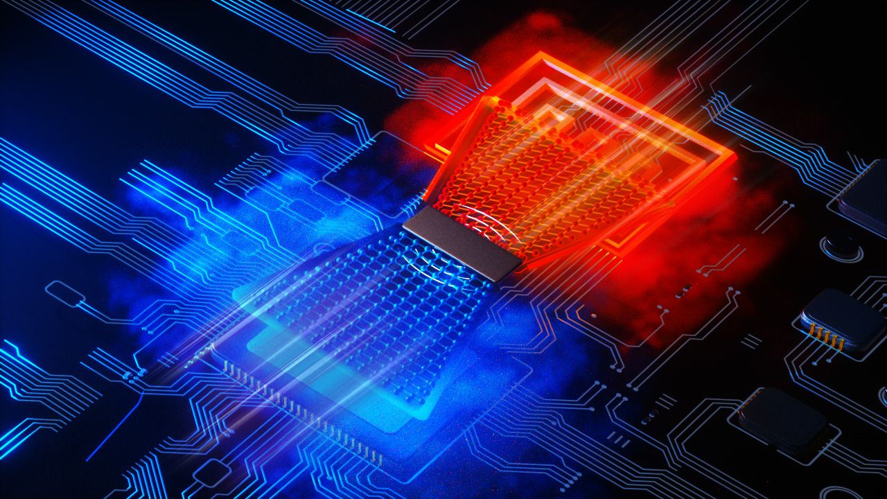
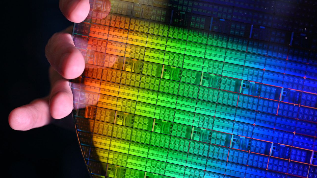
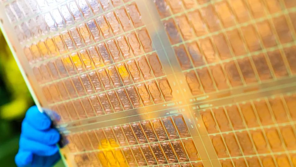
In an unexpected turn of events, Terafab has faced an odd roadblock as a small U.S.-based company called Tera-Print sent a cease-and-desist letter to SpaceX and Tesla back in May to stop using the Terafab name. The company with tera-scale ambitions has run into a tabletop-sized problem because the Tera-Fab name has already been used for about a decade by Tera-Print, according to PCMag.
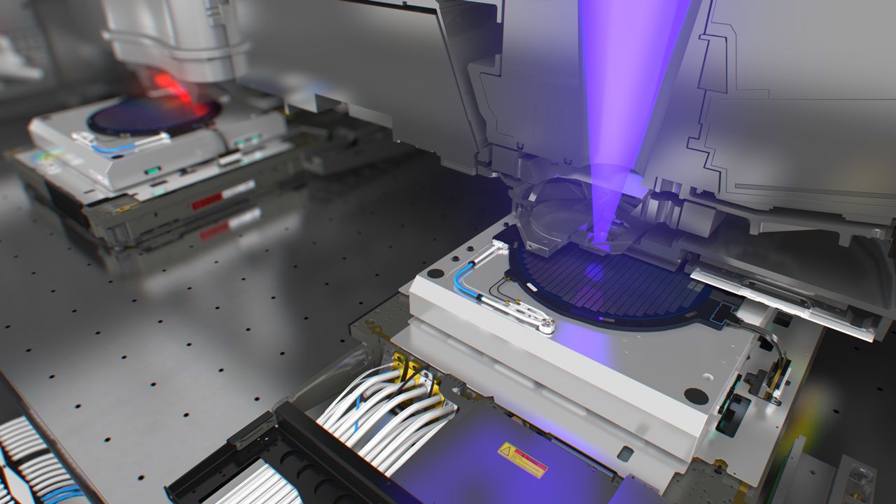
As it turns out, Tera-Print sells tabletop-sized Tera-Fab-branded beam pen lithography (BPL) tools primarily aimed at bioengineering and prototyping of microfluidic devices and has used the brand for about a decade. The U.S. Department of Defense appears to be a client of Tera-print, which uses Tera-Fab.
While Tera-print claims that the Terafab name could be confused with its Tera-Fab product family, Tesla, SpaceX, and SpaceXAI counter that the operations are fundamentally different: Terafab is set to produce chips in extremely high volumes to serve AI, automotive, robotics, and eventually (at least some) space applications, whereas Tera-print's Tera-Fab is a compact lithography tool that can be used for bioengineering or prototyping of electronic or optical devices.
Formally, the trademark coverage puts both names into the same semiconductor technology bucket, albeit with different descriptions:
Tesla's Terafab covers 'custom manufacture of semiconductor chips, memory chips, integrated circuits, and wafers' (IC 040) as well as 'distribution services, namely, delivery of semiconductor chips, chip carriers, namely, semiconductor chip housings, memory chips, integrated circuits, semiconductors, and microchips' (IC 039).
Tera-print's Tera-Fab covers 'Polymer pen and beam pen lithography instruments in the nature of 3D micro-printers and 3D nano-scale printers' (IC 007); 'Polymer pen and beam pen lithography instruments in the nature of 2D micro-scale molecular and material printers and 2D nano-scale molecular and material printers' (IC 009), 'Light-directed photochemical synthesis tools; Industrial advanced materials synthesis tools; Advanced light projection systems; High precision force-feedback sample alignment modules; Environmental control sample chambers' (IC 009); as well as 'training services in the field of AI design and development, electronics, computer science, biology, and material science' (IC 042).
The two companies reportedly entered settlement talks, which included an offer from Tesla, but Tera-Print alleges that Tesla expressed interest in continuing negotiations instead of taking the dispute to court. Tera-Print says it will now defend its registered trademark and argues that the companies operate in related fields, which could lead to confusion.
Even as chipmakers race to build the most advanced chips inside the United States, experts are saying that their efforts are facing one monumental challenge: a massive shortage of skilled workers to run the fabs and factories. According to CNBC, global consulting firm McKinsey and the SEMI Foundation suggest the industry will have up to 157,000 positions that could remain unfilled by 2030.
“I’m concerned,” Samsung semiconductor division EVP Jon Taylor told CNBC in an interview. “We just don’t see that there’s enough technical people in the pipeline.” The McKinsey report says that only 3% of U.S. engineering graduates end up working in the semiconductor industry, and that 73% of chip companies are finding it hard to fill engineering roles. This is a huge contrast to other tech jobs, which saw record layoffs by June of this year, when over 40,000 positions were axed, ostensibly largely due to AI.
The massive demand for memory and storage chips driven by the AI boom, combined with Washington’s efforts to bring semiconductor manufacturing back to the United States, has led to the buildup of multiple fabs and facilities dedicated to it. TSMC was one of the first companies to kick off this building spree, when it started construction on its Arizona campus in 2021. The site started churning out chips last year, with the company committing another $100 billion in July 2026 to build four more 2nm fabs. Intel’s Ohio One plant, which was, at one point, America’s largest fab complex, is also underway, with the site expected to start production between 2030 and 2031.
The big three memory makers — Micron, Samsung, and SK hynix — are also planning or have recently completed major expansions in the U.S. Samsung is starting advanced semiconductor manufacturing in the U.S., with its Taylor, Texas, fab entering risk production this year. The fab is targeting an output of 50,000 wafer starts per month, and it is expected to create 3,500 jobs. “We’re hiring engineers, we’re hiring technicians, we’re hiring people in the supply chain,” Taylor told the publication. “Everybody wants and needs the same thing, and it’s a bit of a race against time right now as everything is starting to come online.”
Micron is also currently building its Boise, Idaho, memory chip fab, which began construction in 2022 and is projected to begin wafer production by 2027. The company has also formally broken ground on its $100-billion New York “megafab,” with aims to produce 40% of its global output within the U.S. by the 2040s. Aside from these massive manufacturing sites, it has also committed $10 billion toward new research labs in the U.S., to be built near the global Micron R&D center in Boise.
Finally, SK hynix also started construction of its first HBM plant in the U.S., with its West Lafayette, Indiana, campus dedicated to packaging these crucial components for AI data centers. There have also been rumors that the South Korean company is in talks with Intel to either lease space at its Ohio One factory or launch a joint venture alongside other AI hyperscalers to build memory chips in the U.S.
All these construction projects, plus the requisite supply chains, will necessitate thousands of workers. Local universities like Purdue University and Arizona State University are already investing millions of dollars to help prepare a capable workforce, with the former launching degrees in 2022 focused on semiconductors. Samsung and Intel are also investing in various programs, including internships and scholarships, to help secure a future workforce for the companies.
However, salary is one major concern listed by the SEMI Foundation. U.S. chip fabs typically pay $127,000 to $187,000, with senior staff getting $238,000 or more. While this is a more-than-competitive salary in the U.S., it’s dwarfed by the bonuses recently offered by Samsung and SK hynix in South Korea, which have reached hundreds of thousands of dollars. With the projected worker shortfall, we should expect the job offers from these semiconductor companies to catch up with their eastern counterparts if they want to secure and maintain talent here in the U.S.
One of the key challenges with the development of extreme ultraviolet (EUV) lithography scanners is building a powerful and reliable light source. ASML, which is the only company to manufacture EUV lithography tools, uses rather complicated laser-produced plasma (LPP) technology to generate EUV light. By contrast, numerous companies propose to use a free-electron laser (FEL), which relies on a particle accelerator, for EUV generation. While FEL has its advantages and is even endorsed by Elon Musk, ASML is unlikely to adopt it, according to JPMorgan.
"Given laser advances, ASML sees no reason to try new 'FEL' light source favored by Musk," reports Semi Doped, citing a JPMorgan note for clients.
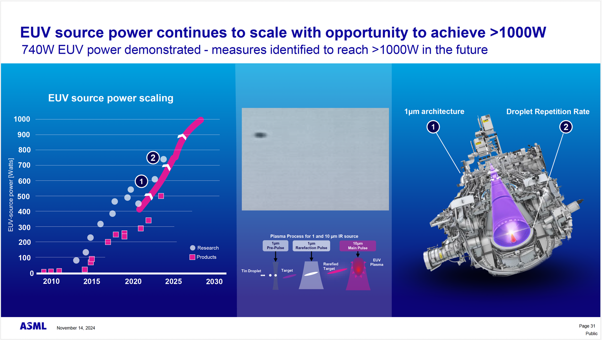
Modern EUV lithography systems use laser-produced plasma light sources that fire powerful CO₂ laser pulses at tiny droplets of molten tin, around 30 microns in diameter, which turns them into ionized plasma with electron temperatures of several tens of electron volts that emits 13.5-nm EUV radiation. The light is then collected by a roughly 0.5-meter elliptical collector mirror coated with multiple layers of molybdenum and silicon, which selectively reflects as much 13.5-nm radiation as possible and directs it toward the intermediate focus at the entrance to the scanner.
Since virtually all materials absorb EUV radiation — even specialized multilayer mirrors absorb a substantial portion of it — the entire optical path must operate in vacuum and use reflective rather than conventional refractive optics, which is one reason why generating sufficient EUV source power remains challenging.
(Image credit: ASML)
Despite major challenges, ASML has gradually increased the source power of its LPP light sources from around 250W to around 500W and plans to increase it to 1000W in the coming years. In addition, the company plans to almost double the number of generated tin droplets to 100,000 every second.
(Image credit: ASML)
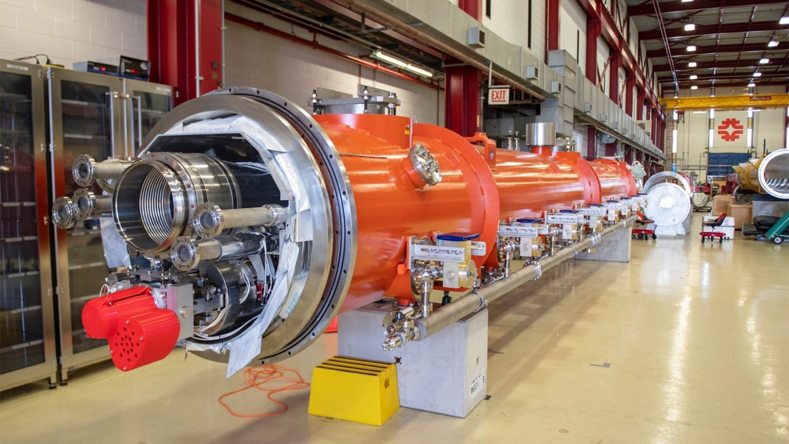
A free-electron laser (FEL) generates EUV light by accelerating electrons to nearly the speed of light and passing the electron beam through an undulator, a series of alternating magnets that force electrons to oscillate and emit radiation. Interaction between the electrons and their radiation causes them to form microscopic bunches and emit light with a 13.5-nm wavelength. This approach eliminates tin droplets and associated debris (that require usage of protective pellicles on photomasks) as well as potentially provides substantially higher EUV power than LPP sources. Furthermore, one FEL can potentially replace multiple LPP sources with a single FEL and a large EUV beam-distribution system.
Yet, there is a major tradeoff: instead of a relatively compact LPP, FEL requires a highly complex particle accelerator, an electron source, a long undulator, electron-beam control, radiation shielding, and an extremely complex distribution system featuring mirrors capable of handling and distributing very high EUV power without losing too much of it along the way. The whole machine must achieve semiconductor fab levels of availability, efficiency, and cost, something that took ASML and the rest of the industry years to achieve.
(Image credit: xLight)
So, while there is a great enthusiasm surrounding FEL in China, the U.S., and Japan, it will likely take a decade, if not more, before FEL will be able to rival LPP in real semiconductor production facilities. The technology will likely devour billions of dollars in the meantime, so not all entities currently pursuing FEL will live that long.
PieceMakers, a Nanya-backed DRAM designer, began trading on Taiwan’s Emerging Stock Board on September 16 at a NT$740 reference price, Cnyes reported ahead of the debut. PieceMakers is not an HBM company. Instead, it bets that inference memory diverges from training memory, President Lee Hsiao-wen told Cnyes, and that DRAM stacked directly on the processor with hybrid bonding can sit between Nvidia’s SRAM-only Groq LPU and HBM. As it stands, design fees, not chips, carry the company's profit, with AI custom-design work accounting for around 40% of the company's revenue in the first half of 2026. Piecemakers Chairman Joseph Ting told TechNews that its first volume customer program will not contribute to the company's financials until 2027 at the earliest.
At roughly 60.4 million shares outstanding, that price values the company at around NT$44.7 billion (around $1.4 billion). Taiwan's Emerging Board is the Taipei Exchange's pre-listing market, not a main-board IPO, so shares trade through market makers ahead of any formal listing application. The stock ended its first session at NT$915, 23.6% above the NT$740 reference price, after opening at NT$1,035 and trading as high as NT$1,205.
Nanya Technology is the largest holder of Piecemakers, at 33.96%, after selling 715,000 shares at NT$740 to seed the float, a disposal it disclosed in a Sept. 9 exchange filing reported by Knews.
What PieceMakers sells
PieceMakers was founded in January 2006 in Hsinchu, Taiwan, led by chairman Joseph Ting and president Lee Hsiao-wen. Historically, the company has designed standard SDR/DDR DRAM and known-good-die (KGD) parts through representatives in China, Japan, France, Turkey, and Israel. Now, the company seeks to shift from direct product sales to custom design services, paid as non-recurring engineering (NRE) fees, and then to IP licensing, royalties, and turnkey production from 2027, the company said at its Sept. 7 briefing, UDN reported.
Revenue from the AI custom design unit has risen from around 4% in 2024 to almost 40% in the first half of 2026. The products behind that increase are HBLL (High Bandwidth, Low Latency RAM), a 2D die rated at 144 GB/s that was taped out in 2016 for Intel’s HPC line and published at ISSCC in 2017, and HiBaLL, the 3D-stacked version rated at more than 1 TB/s, the company claims.
The company described its customers to Cnyes as developers of cloud AI inference accelerators, international semiconductor players, and North American customers, with some programs in design and verification, and none named. Qualcomm CEO Cristiano Amon’s Computex keynote backdrop in June listed PieceMakers among Taiwan ecosystem partners, although neither company has defined the relationship. The takeaway is that the profit is in design fees and not chips. The margin curve matches a pre-royalty Non-Recurring Engineering (NRE) business, rather than a traditional memory vendor.
Why Nanya is chasing this instead of HBM
Nanya’s AI-memory strategy is custom and edge rather than HBM3E. PieceMakers is the first half of a strategy laid out in 2024. On Aug. 7, 2025, Nanya announced a joint venture with Etron Technology, a Hsinchu-based chip designer, capitalized at NT$500 million, with 80/20 ownership. The venture was envisioned to design custom high-bandwidth memory for edge AI devices rather than for data center accelerators. Nanya president Pei-Ing Lee said earlier in 2025 that the company would not compete in HBM3 or HBM3E, TrendForce reported.
Both halves of the strategy rely on Formosa Advanced Technologies, the Formosa Plastics Group’s test and assembly affiliate, for packaging. It is building the through-silicon-via (TSV) and die-stacking processes that both need. The surge in DRAM pricing has made commodity memory Nanya’s real business, which leaves PieceMakers a cheap side bet that has become a windfall. Nanya took advantage of this by selling around 3% of its stake in a move that suggests it is acting more as an investor than a parent building a memory stack.
The inference gap
Groq is an AI inference startup that Nvidia struck a $20 billion licensing-and-talent deal for on Dec. 24, 2025. Nvidia announced its first chip built from that, the Groq 3 LPU (language processing unit), Nvidia’s SRAM-based inference chip, at GTC, its annual developer conference, in San Jose earlier this year.
There is no HBM or DRAM on the Groq 3 LPU. Instead, it uses 512MB of SRAM on the die to deliver 150 TB/s of bandwidth against 22 TB/s from the 288GB of HBM4 on each Rubin GPU. It’s a decode-only co-processor with Rubin handling the prompt prefill, displacing Nvidia’s Rubin CPX from the roadmap.
At Hot Chips 2026, Nvidia’s Igor Arsovski, Groq’s former chief architect, said the rack is in production and published the first third-party benchmark: 3,431 tokens per second on a 100K-context, 31B-parameter model, at about four times the next-fastest public endpoint, in a single-request test that wenoted isn’t directly comparable to the shared endpoints it was measured against. The cost is capacity: at 512MB per chip, a 256-LPU rack holds 128GB, with the model needing 62 chips at FP8 just to hold the benchmark weights. Nvidia accepted that trade for decode speed, which supports Lee’s point that the market leader’s newest inference product contains no HBM.
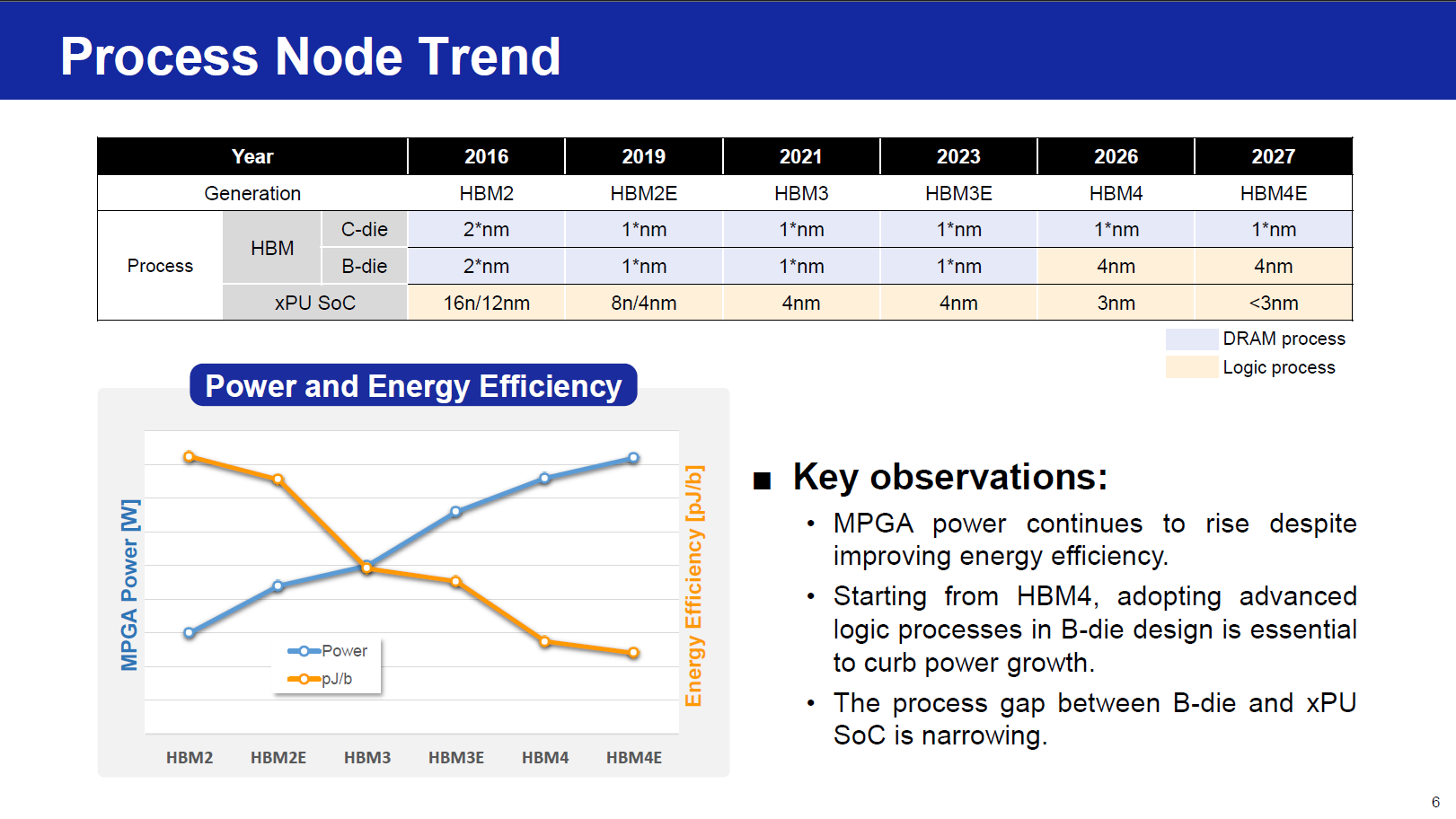
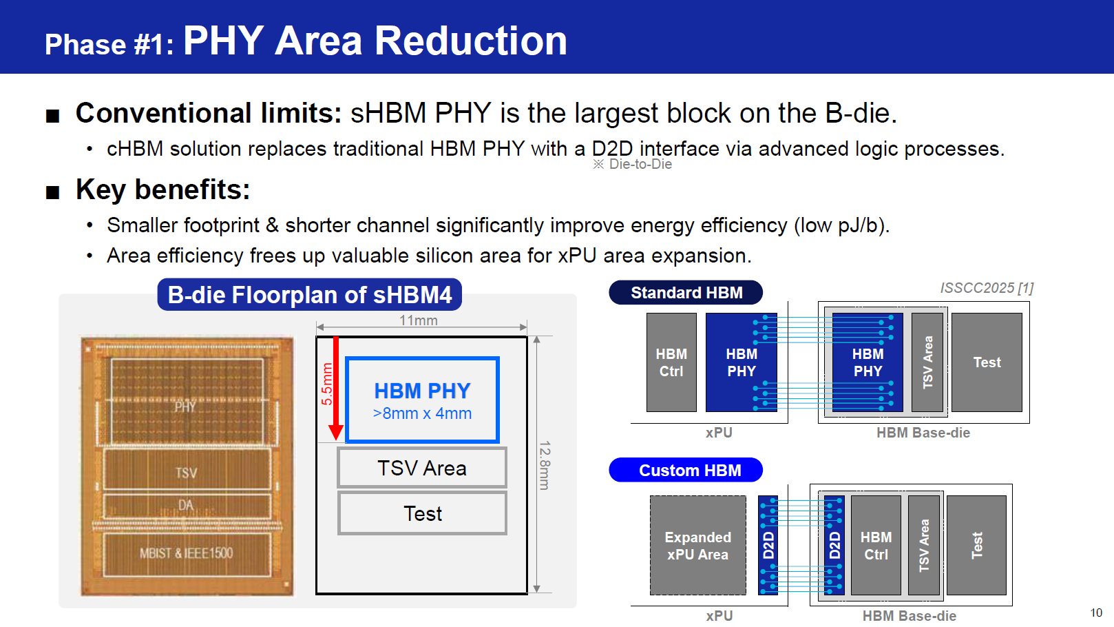
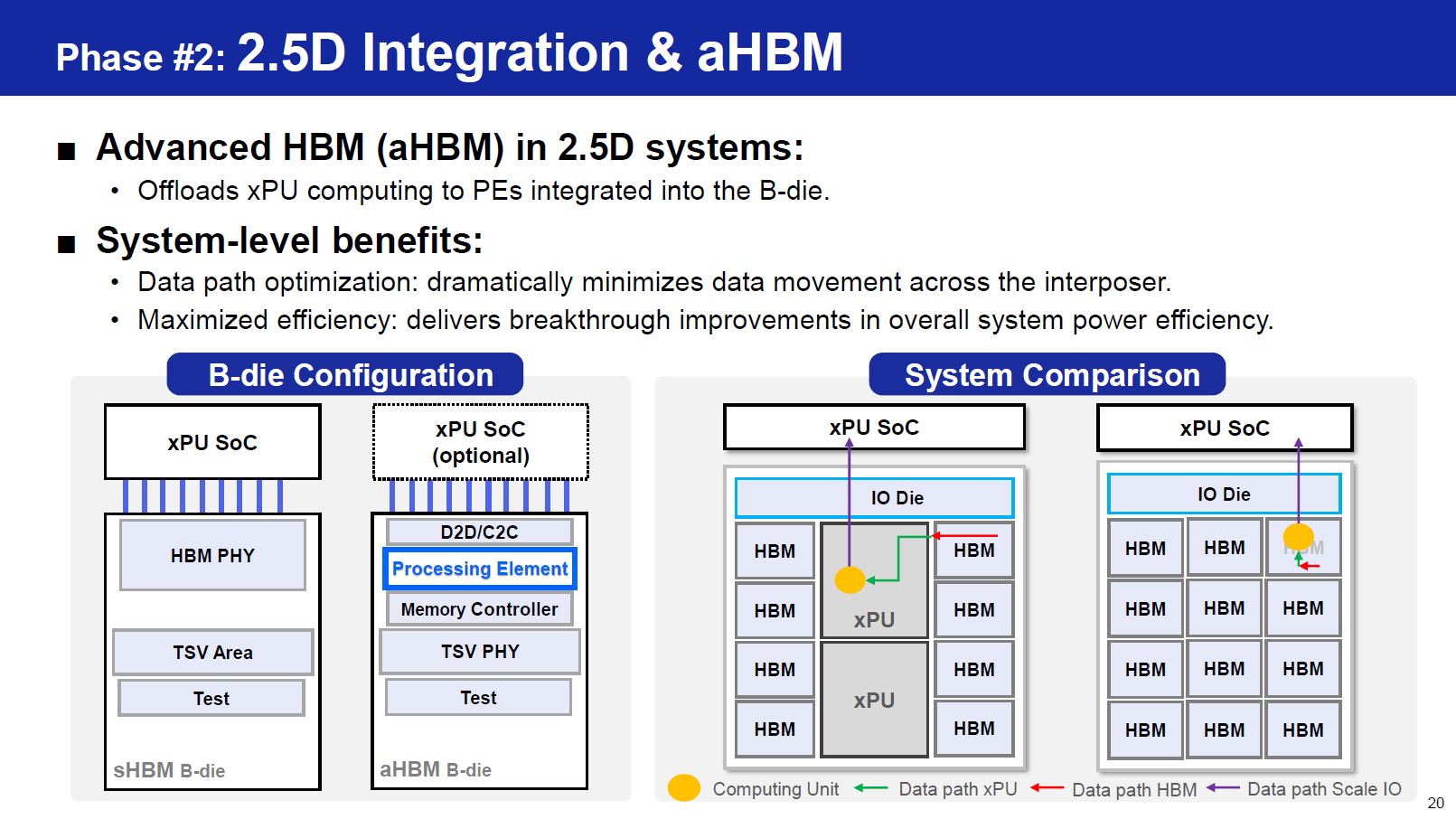
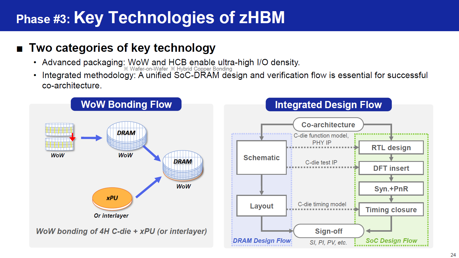
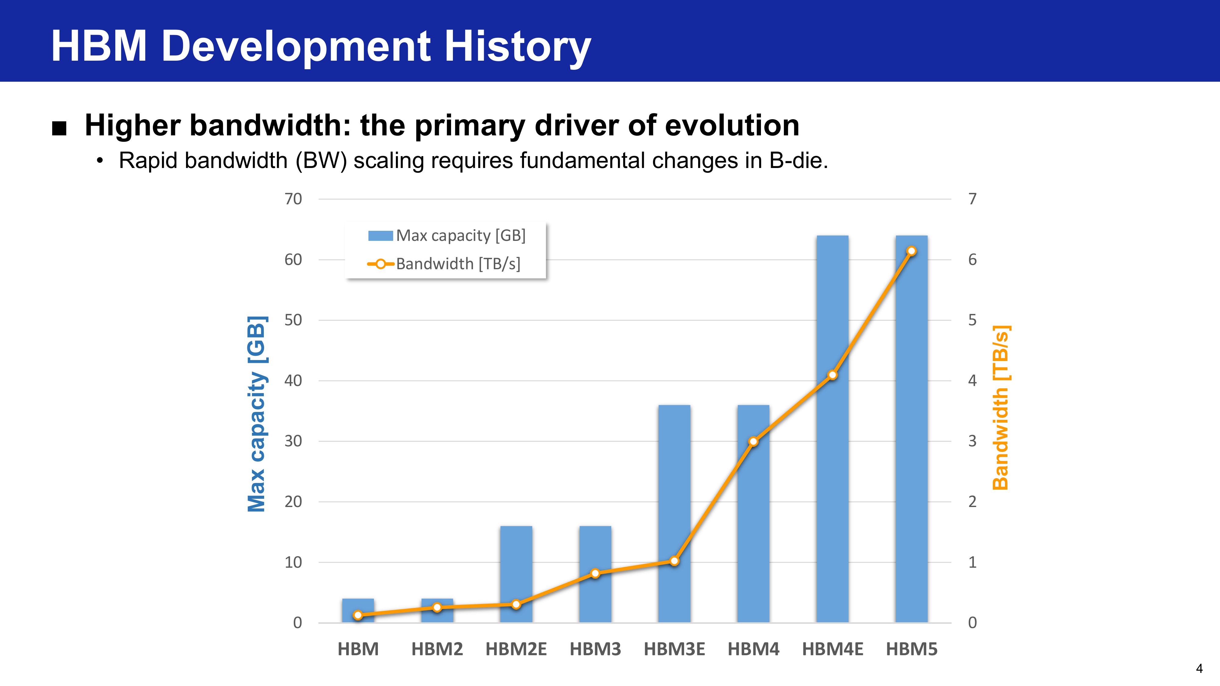
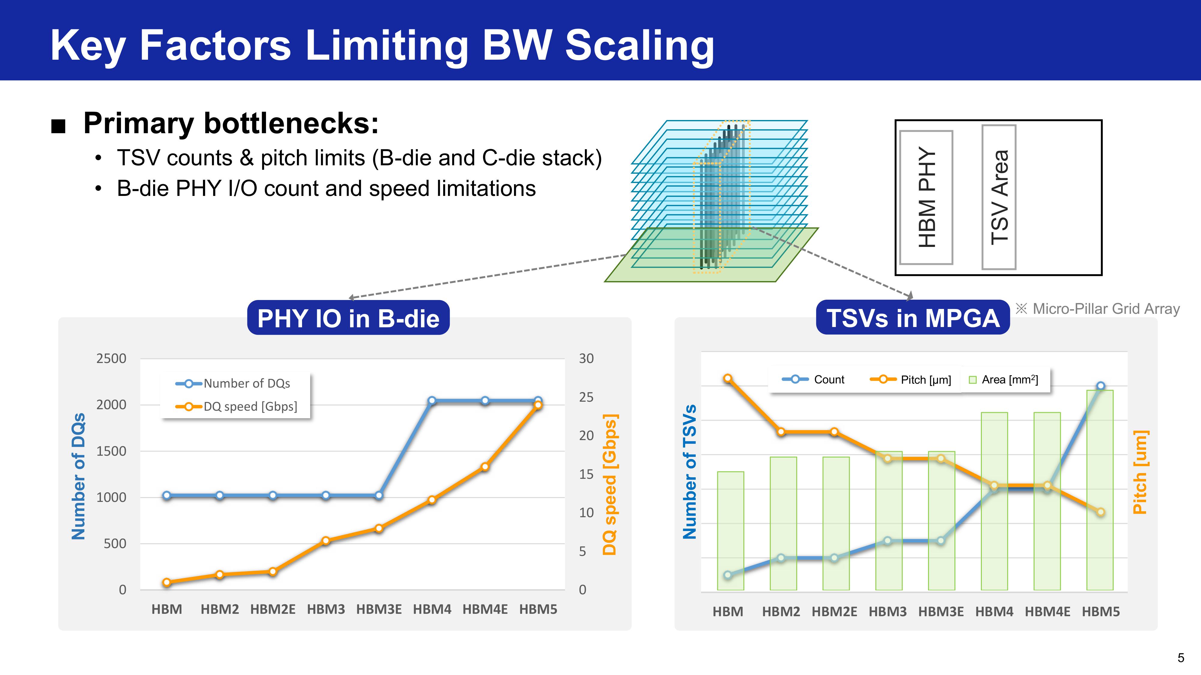
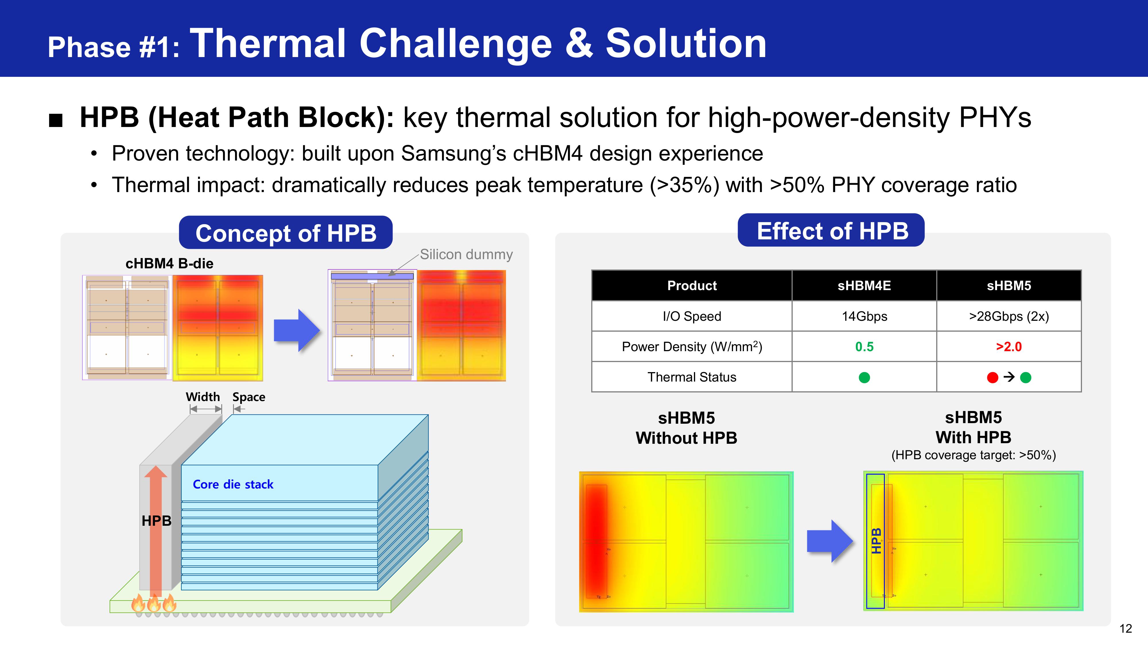
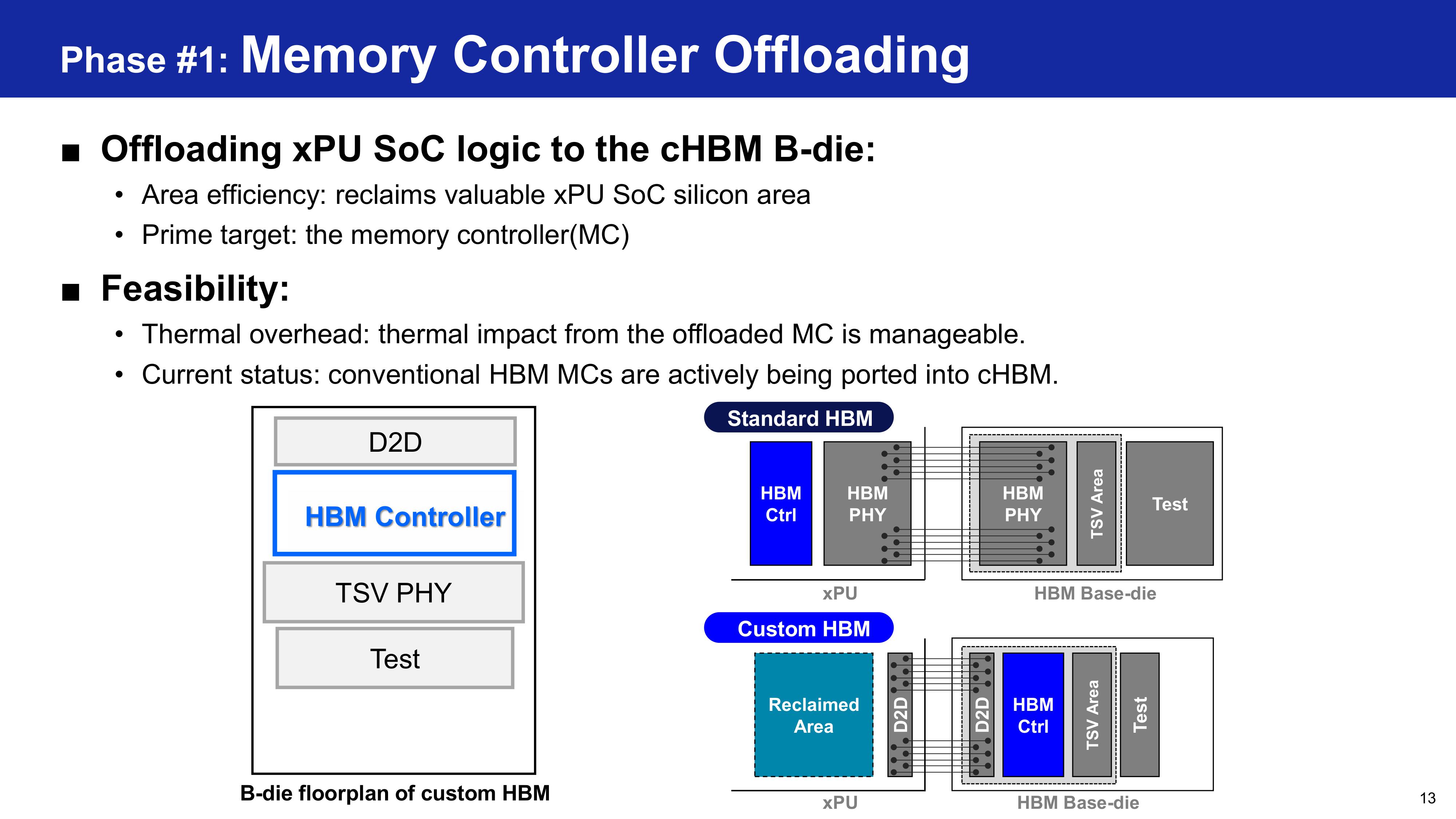
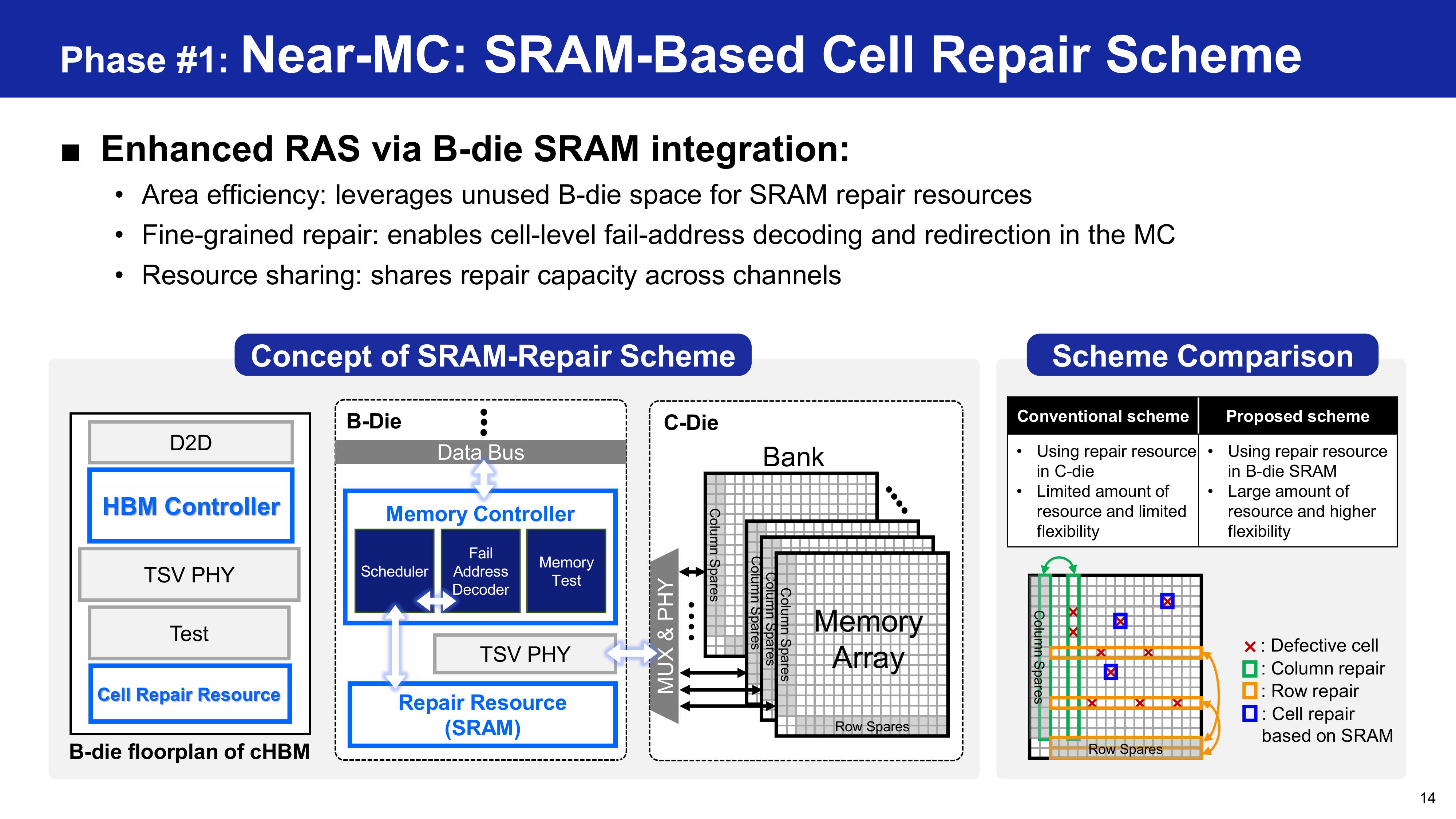
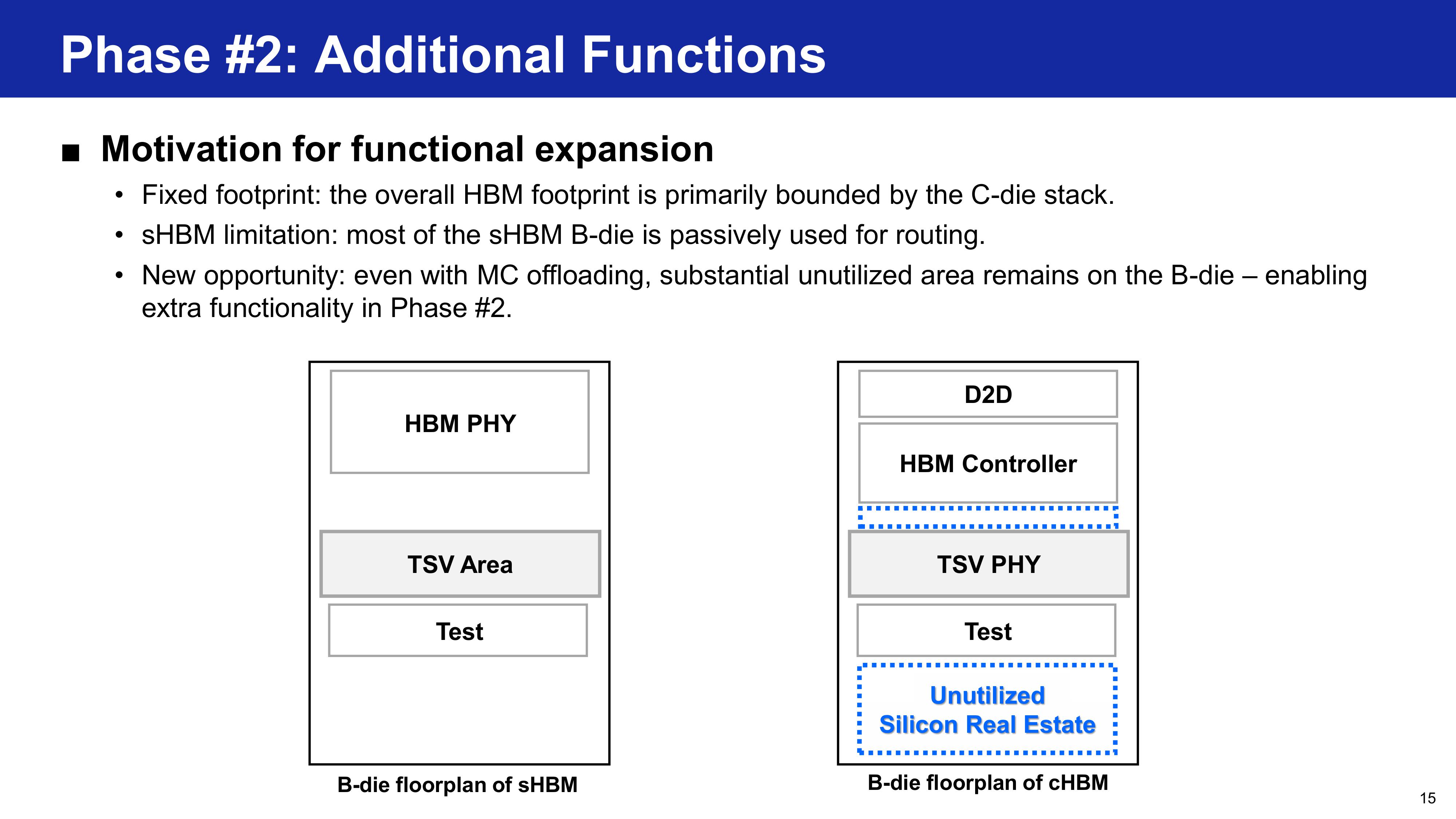
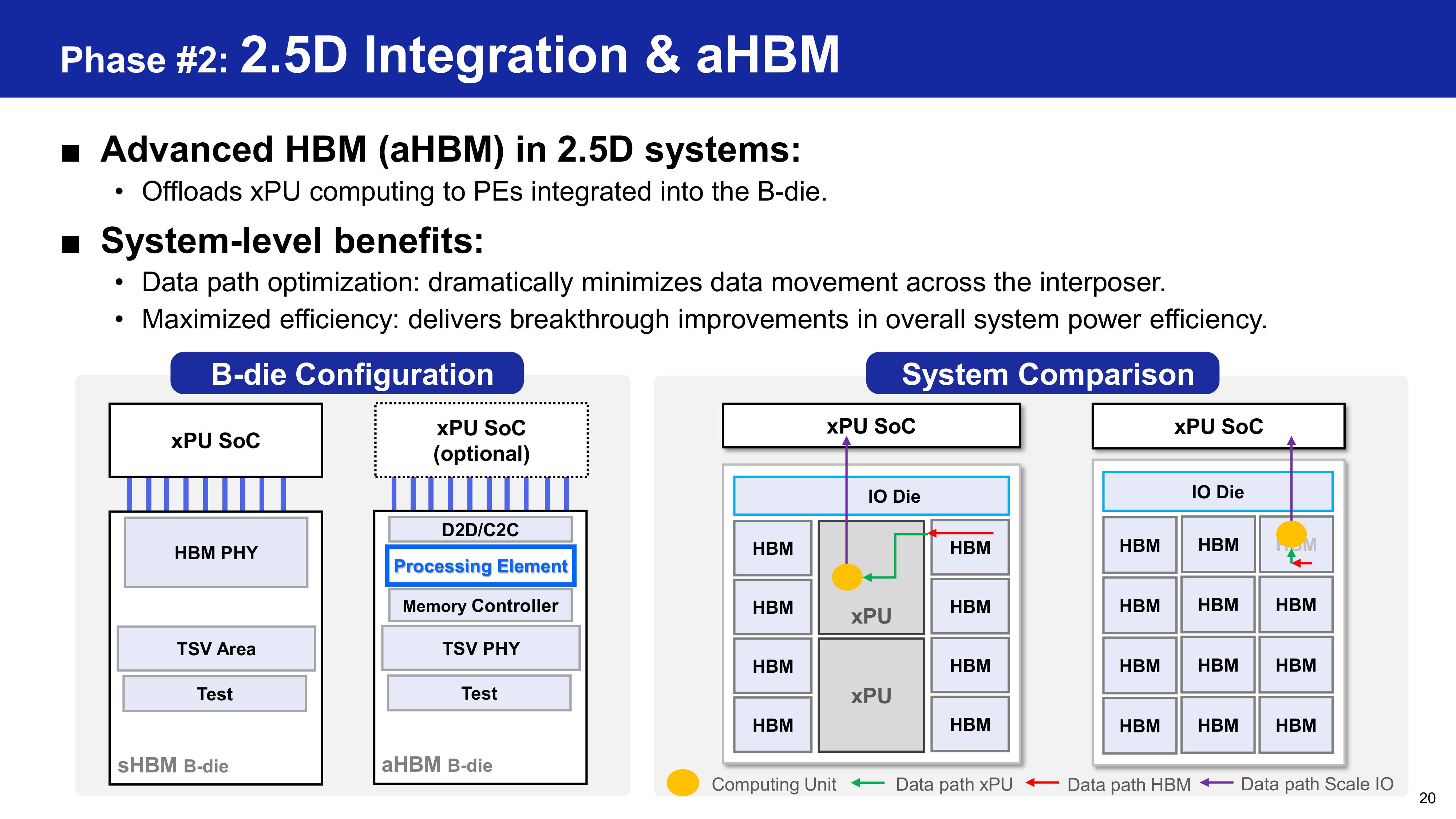
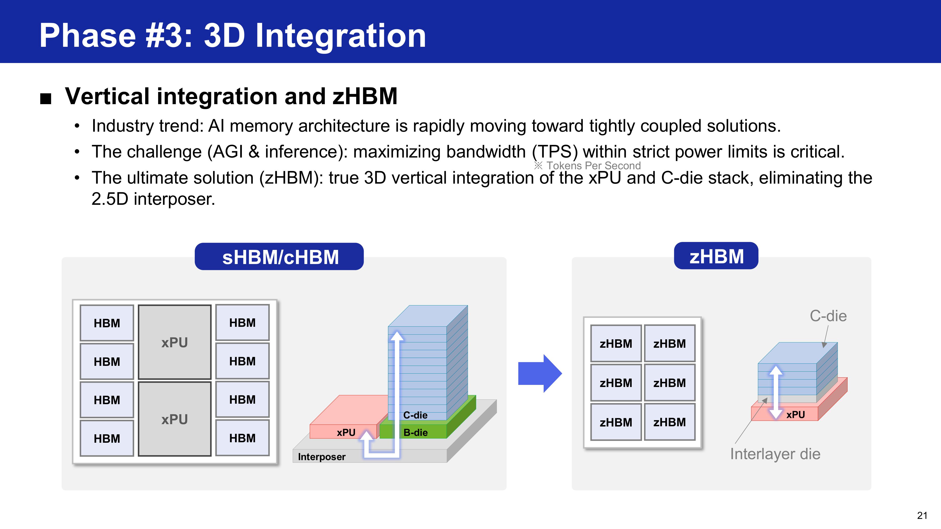
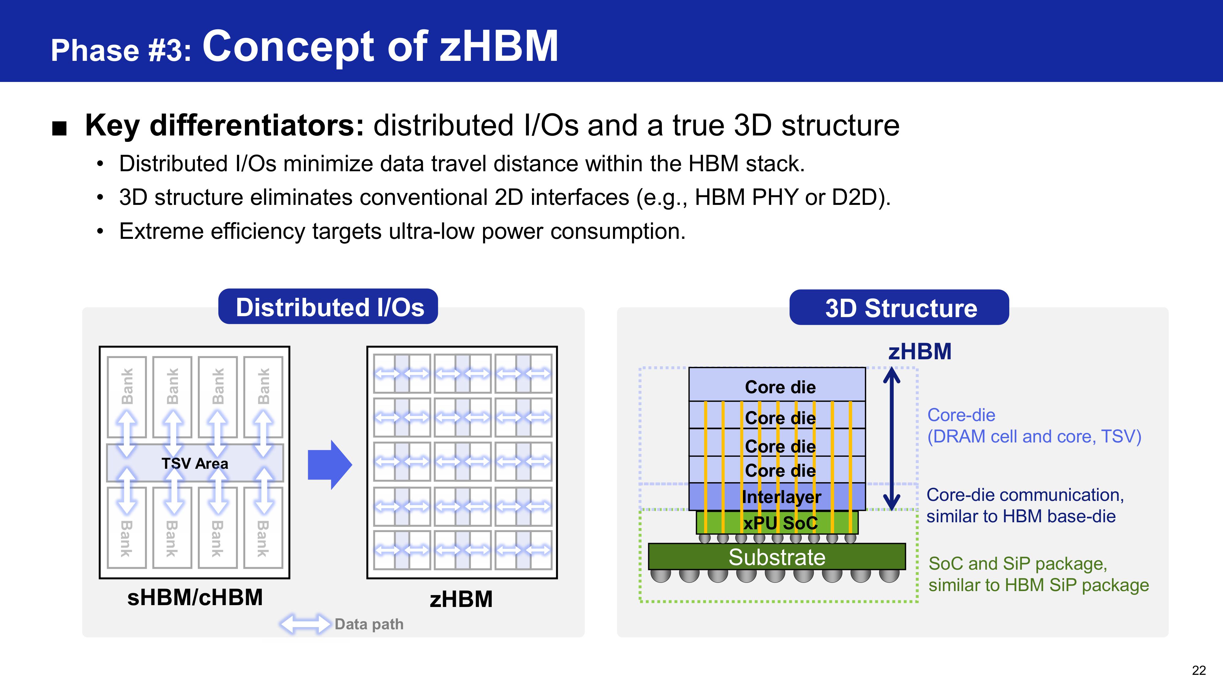
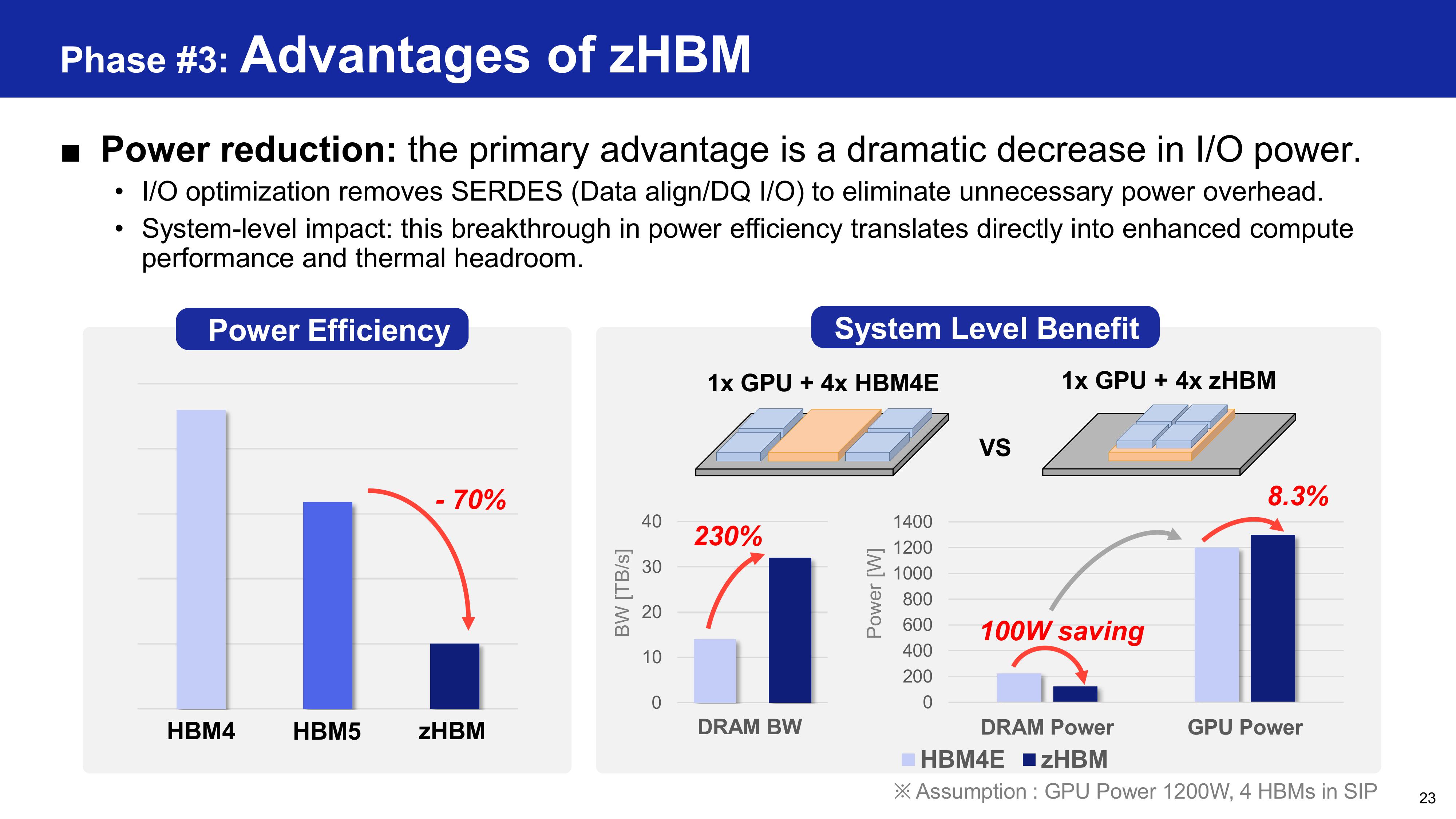
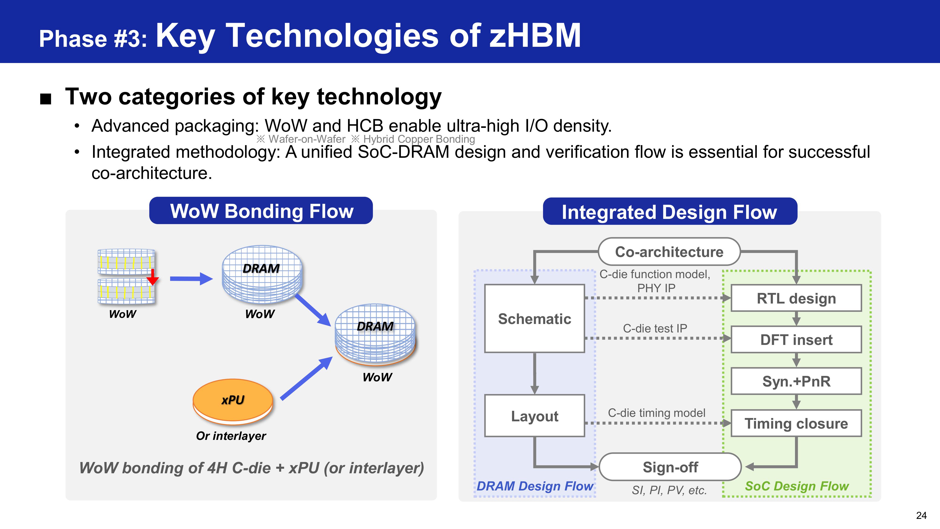
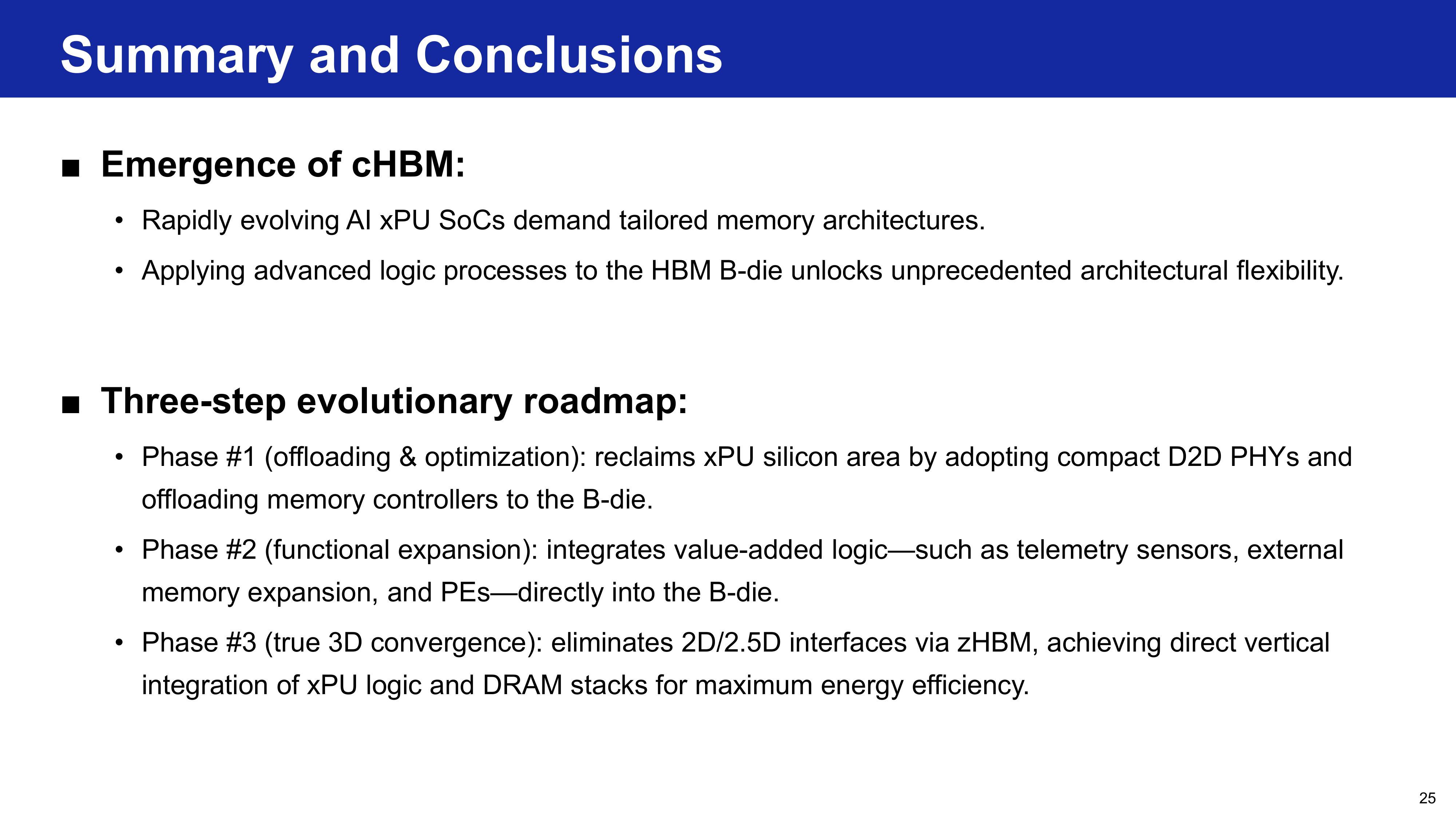
At Hot Chips, Samsung’s Sangwook Han laid out a three-phase HBM roadmap that ends in zHBM, which is DRAM stacked directly on top of the processor rather than beside it on an interposer. Samsung projects about 70% less I/O power usage than HBM5 with roughly 2.3x the bandwidth of a four-stack HBM4E system, with zHBM’s stacks limited to about four-high due to heat, at around 100W less. This would require wafer-on-wafer hybrid copper bonding and tight co-design between DRAM and SoC teams. SK hynix’s Jaesik Lee, VP of package engineering, said on Aug. 23 that hybrid bonding won’t be ready for HBM4E, leaving HBM5 as the earliest point. Counterpoint Research expects full-scale HBM production with the technique around 2029–2030.
PieceMakers offers a different version. Instead of the GPU-plus-HBM 2.5D layout, it bonds the DRAM stack directly onto the processor, wafer-on-wafer, with hybrid bonding instead of microbumps. This fits far more connections with the finer pitch, improving bandwidth, and the shorter path reduces both latency and power consumption. The company puts its wafer-on-wafer product at more than 2 TB/s per layer with latency under 20ns, the company figures, but the target is more capacity than SRAM at a lower cost and power than HBM. PieceMakers is not doing the TSV or hybrid bonding itself, as this is handled by the customer’s logic wafer foundry, Ting added. This custom service promises a 2027 date against Samsung's undated roadmap end and SK hynix's HBM5-at-the-earliest timing. Nvidia and Samsung have each, in their own way, settled the architecture question, with the open question being the customer.
Yield is the product
Lee also said that yield is the biggest hurdle to wafer-on-wafer mass production. The repair architecture has to be designed in, with testing before bonding, after bonding, and then after logic integration. Lee’s own example was 80% yield per layer, at which four layers come out at about 41% and eight at 17%. Our recently-published hybrid bonding state of play covers the process side in more detail.
This better puts into perspective why the company sells repair and known-good-die IP as much as it does bandwidth. It’s also why an IP-and-royalty model fits the strategy — yield IP is portable across customers while a bandwidth number is not.
What to watch
For PieceMakers, AI revenue remains primarily NRE until there is a first named customer, with the first volume program expected in 2027 at the earliest. Ting said that Nanya’s Q3 2026 results, which come in late October, will gauge the PieceMakers gain and reveal further financial information. SK hynix’s hybrid-bonding timing, which targets HBM5 at the earliest, is the current benchmark, although its 16- and 20-layer memory stacks are a separate problem from a few DRAM layers on a logic wafer. Qualcomm may also describe its relationship with PieceMakers more formally.
PieceMakers is likely to end up as an IP licensor with a small number of accelerator customers and turnkey volume through Nanya and Formosa Advanced Technologies. The technology risk is the foundry’s and the customer’s, which is why PieceMakers’ design-fee model works. PieceMakers is expected to benefit from a 2027–2028 ramp, later than Ting’s 2027. If the largest HBM maker won’t bond its own memory this way before HBM5, PieceMakers’ own 2027 date is the one it must meet.
China's progress toward technological self-sufficiency in recent years is undeniable, but there is one thing that the country has so far failed to develop: lithography tools that are on par with those offered by ASML. That shortcoming has greatly hampered its domestic semiconductor industry. But Nvidia CEO Jensen Huang believes China will develop its own advanced lithography systems in just three or four years.
"They are going to get there by 2030," Huang said in an interview with The All-In Podcast (at 43:43). "2030 is just around the corner. The way to think about China is that it is really good at high-volume production. It is just a matter of time[...] so two or three years is just a click; it is nothing. So as far as they are concerned, they are already there."
Huang tends to look optimistically at China's technological development. Specifically, he is known for calling China's AI industry as being 'right behind' American frontier labs, which may well be correct, given how much capital China is investing in AI. But when it comes to the Chinese semiconductor industry in general and its lithography sector in particular, Huang may be too optimistic.
At present, China's leading producer of lithography tools — Shanghai Micro Electronics Equipment — can mass-produce a 193-nm ArF dry scanner that can be used to build chips on 90nm-class process technology. While the company has reportedly developed a 28nm-capable ArF immersion scanner, there is no public evidence that such systems are produced in volume and are used for high-volume chip production.
Although there are reports that Shanghai Aishengna Electronic Technology Group (a unit, or an affiliate of SMEE) has delivered its first immersion scanner that may be capable of printing chips using 28nm-class process technology, these tools will require extensive qualification before they can be used for high-volume manufacturing of semiconductors, so if deployment follows standard timelines, it will take years before this unit will be used for mass producing chips.
Even assuming that the first scanners are delivered to Chinese chipmakers in 2026, widespread production use before 2028–2029 appears unlikely. Furthermore, matching the capabilities of an early-generation ASML immersion scanner would still leave Chinese lithography suppliers considerably behind ASML's contemporary systems, which makes technological parity in ArF immersion lithography by 2030 highly unlikely.
China is considerably further behind in extreme ultraviolet (EUV) lithography. While there are reports that Chinese scientists have managed to develop a laser-produced plasma source that can generate the 13.5-nanometer wavelength light required for the technology, it does not look like China is close to assembling even a prototype EUV scanner itself.
Even if China can assemble an EUV experimental exposure platform without having mastered production-quality immersion DUV, it is hard to imagine a Chinese company producing EUV scanners without solving the hardest problems common to both DUV and EUV technologies. A production lithography scanner requires extraordinary capabilities in wafer and reticle stages, alignment, overlay, projection optics, and metrology, just to name a few.
If China is still struggling to industrialize these capabilities for immersion DUV, there is little reason to assume it has somehow solved them at the substantially more demanding EUV level. But given the potentially existential stakes of the AI race, and the determination of the Chinese government to achieve technological self-sufficiency, it may just indeed be a matter of time.
South Korean memory chip manufacturer SK hynix is in talks with Intel to start manufacturing inside the U.S., according to Reuters. The company is reportedly considering multiple options, including leasing space at the under-construction Intel Ohio One site and forming a joint venture with Intel and other AI hyperscalers desperate for HBM.
This move could help alleviate the memory shortage. It would also complement the company’s expansion in Indiana, where it recently broke ground on an HBM packaging plant a few weeks after its historic $26.5-billion Nasdaq listing. It’s unclear yet if these talks are part of the results of the South Korean president’s visit to Silicon Valley in an effort to expedite negotiations between its top tech companies and their U.S. counterparts, but SK Group chairperson Chey Tae-won told reporters in July, “I think we need to build a factory in the United States. If possible, I believe we should build it.”
However, there are also concerns that Seoul might object to such investment. The South Korean government just unveiled a $520 billion investment plan to increase chipmaking capacity within its shores and keep the country competitive in the AI race; at the same time, it’s also in talks with the U.S. to finalize its $350 billion investment commitment to Washington to reduce tariffs on South Korean goods, $200 billion of which is still undecided on which projects it will be deployed on. Meanwhile, the Commerce Department has threatened to impose more tariffs on South Korean and Taiwanese tech companies if they fail to invest in U.S. manufacturing. This potentially puts SK hynix at a precarious position, especially as it balances the demands from the White House and the Blue House.
Neither company has confirmed these rumors, though. SK hynix told Reuters that it’s “reviewing various measures, including establishing additional production bases, to strengthen the competitiveness of its memory business,” but “no matters have been determined at this stage.” On the other hand, Intel called them speculation and declined to comment on the matter, only saying that it was continuing to invest in the Ohio project, which is expected to come online between 2030 and 2031.
Micron has announced a one-time cash appreciation bonus of NT$1 million (US$31,650) as part of a broader compensation/reward package for its employees based in Taiwan. According to a Reuters report, the full package — which comes amidst ongoing disputes between the U.S. memory giant and its Taiwanese workforce — will see each employee earn a minimum of NT$1.7 million ($53,809.39).
The company called the payouts the largest rewards package in company history, confirming that more than 60,000 employees globally will receive scaled rewards for fiscal year 2026, “following an extraordinary year for the company.” Across the last four quarters, Micron’s cumulative net income from sales of high-demand memory chips has crossed a staggering $50.47 billion, with its Q3 earnings representing a 346% year-over-year increase. After the announcement, the union representing workers at Micron's Taoyuan plant officially rejected the company's bonus proposal, calling the package a distraction.
Under the announced payout, every Taiwan-based employee who joined the company on or before August 29, 2025, is eligible for the flat NT$1 million cash bonus. Those hired during fiscal year 2026 will receive a prorated amount. For direct manufacturing and production-line workers, the total bonus rewards are equivalent to 35 to 68 months of basic salary. Direct labor employees will receive a minimum total cash compensation of NT$1.7 million (US$53,809), while the average total compensation for junior engineers is projected to reach NT$3.4 million (roughly US$106,250), comprising NT$2.9 million in cash and the remainder in equity grants.
The announcement — which mirrors bonus payouts by Samsung and SK Hynix amid the soaring profits from the AI boom — comes after local unions in Taoyuan and Taichung, representing 10,000 of Micron's 15,000 Taiwan workforce, began threatening a strike on September 1, demanding packages similar to the payouts that will see Samsung employees receive over $300,000 in bonuses. The Taiwanese government stepped in to force a mediation. However, unlike in Samsung's case, which also involved government intervention that narrowly averted a potential strike, the talks fell through on September 4 after both parties failed to reach a consensus, leading Micron to announce the NT$1 million bonus package a week later.
In an official statement following Micron's announcement, the union said the new package "sidestepped" the real discussion about a transparent bonus system. The union is pushing for structural change, including a permanent profit-sharing model in which 15% of the company's operating profits are allocated directly to workers and distributed quarterly. They are also demanding a larger one-off payment equivalent to roughly 83 months of salary for fiscal year 2026. Last September, South Korea’s SK Hynix reached a settlement with its union to allocate 10% of annual operating profit directly to employees as performance bonuses for the next decade, eliminating bonus caps.
Similar incidents have played out across the semiconductor industry as companies continue to pull in unprecedented profits from the AI boom. Workers in these industries believe they should share in profits and are requesting concrete institutional safeguards to ensure they are fairly compensated during high-profit AI booms, rather than relying on arbitrary, opaque bonuses decided solely by management. Samsung's unions were ready to strike before reaching an agreement with the company and even held a demonstration attended by over 30,000 Samsung union members.
In the case of Micron — which announced a record-breaking GAAP net income of $28.24 billion in just Q3 2026 — the threat of a strike continues to loom following the Union’s rejection of its proposed payout. A critical second round of mediation is officially scheduled for September 21, 2026. If that upcoming meeting falls apart, the union plans to hold a vote allowing members to strike. In an earlier internal survey, 80% of union members voted in favor of a strike.
Jiangsu Pacific Quartz, a high-purity quartz (HPQ) producer from China, is already supplying its HPQ material to leading domestic and overseas producers of chipmaking tools, including Lam Research and Tokyo Electron. More recently, the company's materials/components have passed certification by a domestic DRAM manufacturer. Analyst TP Huang, who hosts the China Tech Talk podcast, believes that the DRAM maker is CXMT.
While Pacific Quartz's achievements are significant, the company's components are used in semiconductor production equipment after the silicon wafer has been made. Meanwhile, Ingots for semiconductor wafers are grown in crucibles made from high-purity fused quartz, typically over 99.999% SiO₂ (5N+), with much tighter limits on individual critical contaminants. For now, such quartz can only be obtained in significant volumes from Sibelco and The Quartz Corp., which operate in Spruce Pine, North Carolina, and from Russian Quartz LLC, which can produce modest volumes.
Pacific Quartz has supplied Lam Research and Tokyo Electron with ultra-high-purity quartz consumables, such as LPCVD diffusion tubes, wafer boats, quartz ingots, quartz plates, and high-purity quartz tubes, since 2019–2020. Typically, quartz used for process equipment is 4N5 – 5N purity (~99.995–99.999% SiO2). So Pacific Quartz's products are good enough for semiconductor tools.
More recently, Pacific Quartz said its quartz products manufactured from its own high-purity quartz sand passed qualification at a leading Chinese DRAM manufacturer, apparently CXMT, for use in 300-mm wafer production. This is particularly significant because it demonstrates a largely domestic supply chain for Chinese quartz that starts with Pacific Quartz's purified high-purity sand, which is then processed into semiconductor furnace-tube material that goes to a DRAM fab. While CXMT certainly uses equipment from Lam Research and Tokyo Electron, we cannot say for sure that all the quartz consumables that these tools use are made by Pacific Quartz.
Semiconductor furnace tubes are typically made from roughly 5N-class high-purity fused quartz, with stringent limits on electrically active and mobile contaminants, as they can migrate onto/into hot silicon wafers and alter transistor characteristics, ultimately creating defects and lowering yield.
While China-based Pacific Quartz can produce components for semiconductor production equipment, it still cannot produce crucibles good enough to grow silicon wafers with 9N–11N purity. Will it change in the foreseeable future? Only time will tell.
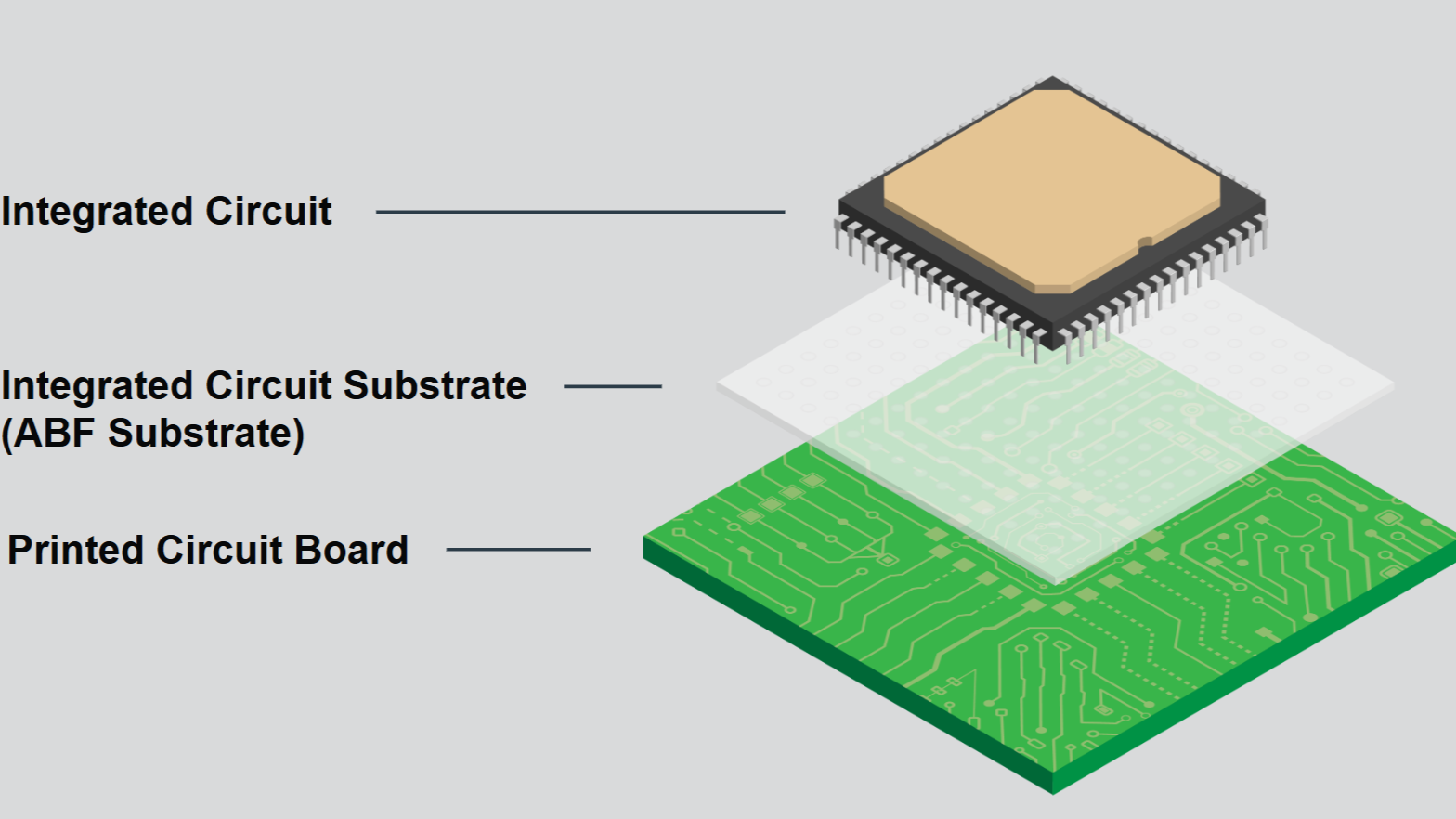
ABF substrates, the specialized insulating and wiring bases that connect tiny silicon chips above them to the much larger printed circuit boards below, sit beneath most high-end CPUs, GPUs, and AI accelerators. Featuring the Ajinomoto build-up film (ABF), these substrates have been critical to the semiconductor industry since the late 1990s, with personal computers, workstations, servers, and networking silicon driving steady demand for decades.
The artificial intelligence boom has multiplied that demand exponentially. Training and inference for frontier models now run across data centers, each housing hundreds of thousands of accelerators and providing hundreds of megawatts of compute. Nvidia alone shipped an estimated 3.2 million Blackwell GPU packages through the end of 2025, with every one of those accelerators packaged on an ABF substrate. Meanwhile, the industry is already entering the gigawatt era with humongous data center buildouts, each expected to house millions of AI accelerators.
This edifice rests on a remarkably narrow supply chain. Practically every advanced logic and AI chip made today by Intel, AMD, and Nvidia depends fundamentally on ABF substrates. These substrates are the conventional default for high-performance packaging. They are made by a small group of specialists, including Unimicron, Ibiden, Kinsus, Shinko Electric Industries, Samsung Electromechanics, and Nan Ya PCB. The upstream supply chain gets much tighter.
The one common denominator across ABF substrates, regardless of manufacturer, is the Ajinomoto build-up film itself. Each substrate maker laminates its build-up layers using dielectric film supplied by Japan's Ajinomoto, which controls a reported 95% or more of the global market. A single company, better known for food seasoning than microelectronics, sits at the base of one of the most concentrated supply chains in computing, almost singlehandedly supplying a material for hundreds of millions of semiconductor devices. Not surprisingly, demand is now growing beyond what the supply chain can comfortably supply.
Compounding this crunch, modern AI accelerators now pack multiple compute, memory, and supporting components onto a single board. As a result, the substrate is getting larger across the X-Y footprint to accommodate the expanding package. Manufacturers are also adding more build-up layers to the substrate to route the growing number of signals and power connections. Each additional layer requires another ABF layer, further multiplying demand across millions of accelerators and extending manufacturing times.
Unfortunately, the complications don't stop there. Beyond further straining the supply chain, expanding the substrates is creating technical problems, such as warpage, yield issues, and electrical losses within the component itself. This leaves the ABF substrate ecosystem facing two related challenges: producing enough advanced substrates for a rapidly expanding fleet of AI accelerators, while simultaneously re-engineering these substrates so they can continue to scale without becoming unmanufacturable or impractical.
The ABF substrate roadmap is consequently as much about supply-chain capacity as it is about the hardware itself, with suppliers such as Ajinomoto and Ibiden outlining plans to expand material and manufacturing capacity, respectively. At the same time, the wider industry — Intel, Samsung, and SK's Absolics among them — is exploring glass-core substrates and other material technologies to push past the limits of organic ABF.
ABF substrates
Silicon dies, including CPUs and GPUs, cannot communicate directly with the printed circuit board beneath them. The connection pads on a die are spaced micrometers apart, while the traces on a motherboard are spaced hundreds of micrometers to millimeters apart. Every high-performance chip, therefore, sits on an intermediary package substrate — a dense, multilayer board that fans the ultra-fine connections on the die outward into connections large enough for the motherboard to handle, while also providing signal routing, power and ground distribution, and mechanical support for the package.
ABF substrates used in AI accelerators typically consist of a rigid, glass-reinforced resin core sandwiched between successive build-up layers of copper wiring and insulating film. The core provides much of the mechanical rigidity, while the layers provide the increasingly dense wiring required close to the silicon.
To create the substrate, the manufacturer laminates the ABF dielectric onto the structure, forms microscopic vias — commonly with a CO2 laser — and then uses lithography and copper deposition to create a new wiring layer. High-end substrates typically use a semi-additive process (SAP), in which fine copper traces are plated up from a thin conductive seed layer. Another ABF layer is then laminated over it, and the process repeats. The film electrically separates successive copper layers, while plated microvias connect them vertically.
ABF substrate (Image credit: Ajinomoto)
Ajinomoto developed the film in the 1990s, after which it gradually became the industry default for its low dielectric loss, fine-line capability, and smooth lamination. The company reportedly accounts for roughly 95% of the substrate film market, with its nearest competitor, Sekisui Chemical, holding only a low-single-digit share.
The manufacturing tier above the film is more populated but still concentrated. Unimicron, Ibiden, and Shinko together account for roughly three-quarters of the substrate market by most estimates, with AT&S and Nan Ya PCB rounding out the leading group. These companies take ABF and other materials and manufacture the finished multilayer substrate. Semiconductor packaging companies, such as TSMC and Amkor, then integrate those substrates into packages containing the processor, memory, and other components.
AI accelerators are pushing substrates outward and upward
To deliver the compute and memory bandwidth that frontier models demand, the industry is packing ever more silicon onto each AI accelerator. Designers now place multiple large logic dies alongside a growing number of high-bandwidth memory stacks on a single package. Nvidia's Blackwell generation mounts two reticle-sized GPU dies and eight HBM3E stacks on a single package, with its upcoming Rubin and Rubin Ultra parts pushing it further still. TSMC's CoWoS packaging is scaling from around 3.3 reticles — each roughly 830 square millimeters of silicon — a generation ago to 5.5 reticles in volume production in 2026, with a roadmap reaching 9.5 reticles in 2027 and beyond 14 reticles by 2029, when a single package is expected to carry roughly ten compute dies and twenty or more memory stacks.
This expansion of the accelerator package is driving the substrate’s expansion on two physical levels. The first expansion is the substrate's footprint in the X-Y axes. The base has to get wider and longer to accommodate the larger package footprint. Ibiden's current roadmap puts its cutting-edge substrate size at 90 × 90mm (3.54 x 3.54 inches) in 2026, 110 × 110mm (4.33 x 4.33 inches) in 2028, and 130 × 130mm (5.12 x 5.12 inches) and larger from 2030 onward. Ajinomoto independently expects the representative advanced AI packages its film goes into to grow from roughly 100 mm² in 2026 to about 120 mm² for 3D AI packages from 2031.
The second expansion is along the Z axis through additional layers. An expanded collection of compute dies and memory creates more signals to route, while the corresponding increase in power draw requires extensive power and ground distribution, all of which must be carried in a growing number of layers. Ibiden's roadmap targets a 10-X-10 buildup structure in 2026, 12-X-12 in 2028, and 14-X-14 from 2030. Here, the numbers represent the build-up layers on either side of the central substrate core: “10-X-10” means 10 build-up layers per side of the core — which is represented by the “X” — each comprising one dielectric layer (ABF) plus one patterned copper layer, working as a pair.
Nan Ya PCB's roadmap points in the same direction. From an 11+N+11 baseline, it targets 24-layer substrates in 2026 and more than 24 layers in the first half of 2027, while tightening line and space from a 9/12 µm baseline to 8/8 µm and then to 6/7 µm by early 2027. Layer-counting conventions differ between vendors, so a per-side figure and a total layer count don't necessarily line up directly.
Nvidia's Blackwell architecture mounts two reticle-sized GPU dies and eight HBM3E stacks on a single package (Image credit: Nvidia)
The substrate’s expansion in both directions creates several challenges. Increasing the X-Y area makes the package harder to keep flat. Silicon, copper, the substrate core, and the polymer build-up materials that make up the substrate expand by different amounts when heated. As the package is bonded during assembly at around 250⁰C and then cooled, these mismatches cause the layers to pull against one another, leading to warping — a problem that becomes harder to control as package dimensions increase.
Excessive warpage can undermine solder-joint formation, layer-to-layer alignment, and reliability, while a larger substrate also occupies more manufacturing-panel area and exposes more area to potential defects. Organic substrates are reported to lose usable flatness once packages exceed roughly 120mm per side, a threshold that the largest AI accelerators are now reaching and that Ibiden's own roadmap — climbing toward 130mm and beyond — is set to cross.
The growing layer count along the z-axis also creates manufacturing challenges around yield, capacity, and time. Every new substrate layer requires a full manufacturing sequence of several steps, all held to sub-ten-micron tolerances. Each added layer increases the chance of a defect or alignment error that can scrap the whole substrate.
Additionally, layer count consumes manufacturing capacity and time in proportion. This is why Ibiden frames future demand in terms of semi-additive processing load rather than a simple substrate count, as a single advanced substrate now consumes far more of a line's capacity than a finished-unit tally would suggest.
Overall, the simultaneous expansion in substrate area and layer count means ABF consumption is rising much faster than processor shipments alone suggest. Ajinomoto illustrated this in its 2025 integrated report with a larger AI substrate that had about 3.5 times the board area and three times as many ABF layers as a conventional design — 18 layers against six — consuming roughly ten times as much ABF overall. This surging material consumption, set against an extremely concentrated supply base, extends the ABF substrate story beyond a technical problem into a supply-chain constraint.
The supply chain constraint
Like many components in the semiconductor industry chain before the AI boom, demand for ABF substrates periodically swung both ways. A severe bottleneck through 2020-2022 — driven by pandemic-era PC and server demand — was followed by an oversupply in 2023, as substrate manufacturers expanded capacity. However, that capacity was built for low-layer-count, smaller consumer substrates, not the large-body, multi-layer packages AI demands.
These advanced products require sufficiently large manufacturing formats, fine SAP wiring, tight layer registration, acceptable warpage, and high yields across much larger structures. Ibiden captures this by measuring demand not in finished substrates but in semi-additive-process load — the actual processing work each part imposes on a line. Indexing 2024 at 1.0, it expects the SAP load of a single AI-server substrate to reach 1.8 times that in 2026 and 2.5 times in 2028, with the company stating that substrate expansion will push total SAP demand beyond industry supply capacity, indicating a constraint in the manufacturing process itself.
The bottleneck is even tighter at the ABF material level. Ajinomoto's film capacity was already running at full load in the second quarter of 2026, at a reported two million square meters per month, although the company has outlined plans to increase capacity. A near-monopoly supplier at full capacity while consumption surges paints a clear picture of the bottleneck’s severity.
Unsurprisingly, prices have moved accordingly. Ajinomoto notified substrate manufacturers in May 2026 that it would raise ABF film prices by approximately 30%, effective in the third quarter. The hike is coming alongside comparable increases in copper-clad laminates from Resonac and Mitsubishi Gas Chemical, compounding pressure across the whole stack. Further tightening the squeeze, Ajinomoto recently cut shipments of the critical ABF film to China by 30%.
Ajinomoto Build-up film (Image credit: Ajinomoto)
The growing ABF substrate problem cannot simply be attributed to Ajinomoto running out of film. In fact, while it's running at full capacity, the company says it has no concerns about its overall supply chain. The constraint stretches across the entire chain containing ABF, glass cloth, and other materials, SAP equipment, large-format substrate factories, yield, and customer-qualified production capacity.
The immense industry demand is progressively tightening the crunch. Several supply-chain analyses converge on an ABF supply-demand shortfall of roughly 10% in the second half of 2026, widening to around 21% in 2027 and potentially exceeding 40% by 2028, with demand for substrate area projected to grow at a compound annual rate near 39% from 2025 to 2028 as accelerators integrate more components.
The roadmap to recovery: more capacity, better materials
The industry is responding to ABF substrates' multifaceted constraints on multiple fronts: expanding manufacturing capacity to relieve near-term supply pressure while qualifying new materials and substrate architectures to break through the technical limits. Capacity expansion is already underway across the supply chain.
Ibiden is executing ¥500 billion ($3.1 billion) in capital investment across fiscal years 2026 to 2028 — the largest single substrate expansion on record — targeting 2.8 times its 2024 capacity for ASIC and AI-server substrates by 2028. Unimicron raised its 2026 capital spending to a record NT$34 billion ($1.07 billion), with a focus on ABF substrates. Meanwhile, Samsung Electro-Mechanics, Samsung's substrate arm, has committed $1.2 billion to expand ABF substrate production, with volume production expected by the third quarter of 2027.
Pegatron's substrate unit, Kinsus, has approved NT$23.5 billion ($722 million) for ABF equipment over three years and now focuses its most advanced lines almost entirely on AI clients, aiming to lift monthly output at its Taoyuan plant by roughly 25% by 2027. While these projects address the shortage directly, their lead times mean the crunch may continue for a while, as supply cannot respond instantly to the AI demand spike.
Ajinomoto is expanding upstream as well. A new plant in Gunma entered full operation in 2025. The company has invested roughly ¥25 billion ($157 million) in ABF production since 2023 and has said it will invest at least as much again by 2030, targeting a capacity increase of more than 50%. It is also adding a third Japanese base for varnish production — envisioned to provide capacity comparable to Gunma — with construction planned for 2028 and operations to begin in 2032.
However, capacity only solves the problem if the current substrate architecture can continue to scale. The material roadmap — aimed at addressing the physical constraints of ABF substrates — is therefore advancing parallel to the factory roadmap. Ajinomoto says present and future ABF generations are being engineered for larger, more multilayered substrates, high-bandwidth I/O, lower transmission loss, and improved resistance to warpage and humidity. The company expects newer, higher-value ABF grades to take an increasing share of its portfolio through 2030.
Substrate makers are addressing the problem from the process side. Nan Ya plans to move beyond 150 mm body sizes and 24 layers while shrinking copper line/space geometry toward 6/7 microns in the first half of 2027. Its materials roadmap includes an ultra-low-CTE core material with a CTE below 3 ppm/°C, alongside low-Dk, low-Df, and low-CTE dielectrics. Finer wiring allows a substrate to support more connections without relying solely on additional area or layers, while low-expansion materials help keep the growing structure flat.
Eventually, the substrate's central core itself may change to glass. Organic substrate cores are increasingly difficult to keep dimensionally stable as packages approach and surpass 100 mm. Glass can be matched more closely to silicon's thermal expansion — providing dimensional stability — and offers substantially lower dielectric loss for high-speed links. It has therefore emerged as one of the industry's main solutions to warpage.
(Image credit: Intel)
As we detailed in our glass substrate roadmap, the move to a glass core is drawing a broad field, as it sits at the intersection of substrate-making, glass manufacturing, and advanced packaging, pulling in chip-and-packaging houses, display and glass specialists, and the incumbent substrate makers alike. Intel demonstrated a package that combines EMIB with a glass substrate at NEPCON Japan in January 2026, although the company still places commercial glass-substrate deployment in the latter half of the decade.
SK Group subsidiary Absolics is operating a low-volume glass-substrate manufacturing facility in Covington, Georgia — backed by $100 million in US CHIPS Act funding — producing prototype and qualification samples for customers, such as AMD for its MI400-series accelerators, while Samsung Electro-Mechanics is producing prototypes on a pilot line in Sejong and now plans mass production through its glass-core joint venture after 2027.
TSMC, meanwhile, is pursuing panel-level packaging through its chip-on-panel-on-substrate (CoPoS) platform, moving to a 310 x 310mm panel format, with a pilot line at its VisEra subsidiary, trial production targeted for 2027 and mass production for the second half of 2028. Glass-core substrates are a separate, later step on TSMC's roadmap, with commercial scale projected after 2030. Ibiden also puts “glass core” on its substrate technology roadmap around 2030 as a solution for warpage control.
The glass core — most likely a late-2020s-to-2030s technology — is positioned as a solution to the warpage wall. It replaces the organic core, not the ABF itself, which would remain the buildup material. A glass core may soften ABF demand per package, as glass's flatness allows finer routing and potentially fewer buildup layers, but it does not remove the material or the dependency. There's the possibility that a future dielectric material will eventually replace ABF, although that doesn't seem to be the industry's main focus currently.
Regardless, the near-term roadmap centers on more advanced SAP capacity, rapidly expanding factories, improved materials, and increased supply. Through the late 2020s, finer wiring, lower-loss ABF, lower-CTE materials, and better warpage control will enable organic substrates to stretch toward 110 mm and beyond. Around 2030, glass cores offer a path toward the 130 mm-plus packages that Ibiden and others already have on their roadmaps.
ASML, Intel, Samsung, and TSMC are teaming up to drive the industry transition to 6×12-inch photomasks (reticles). This shift is paramount for High-NA EUV lithography, as the larger stencil would enable printing large chips in a single pass, instead of having to stitch smaller designs together, as ASML explained in a press release this week.
This kind of collaboration between chipmakers isn't entirely unheard of, but it is rare. But when they face an industry-wide challenge, they set aside their rivalry and join forces to move the industry forward. This happened several times in recent decades, first with the failed transition to 450-mm wafers co-funded by GlobalFoundries, IBM, Intel, Samsung, TSMC, and New York State, then with the EUV transition, which was spearheaded by Intel, TSMC, and Samsung.
Higher resolution comes with a nuance
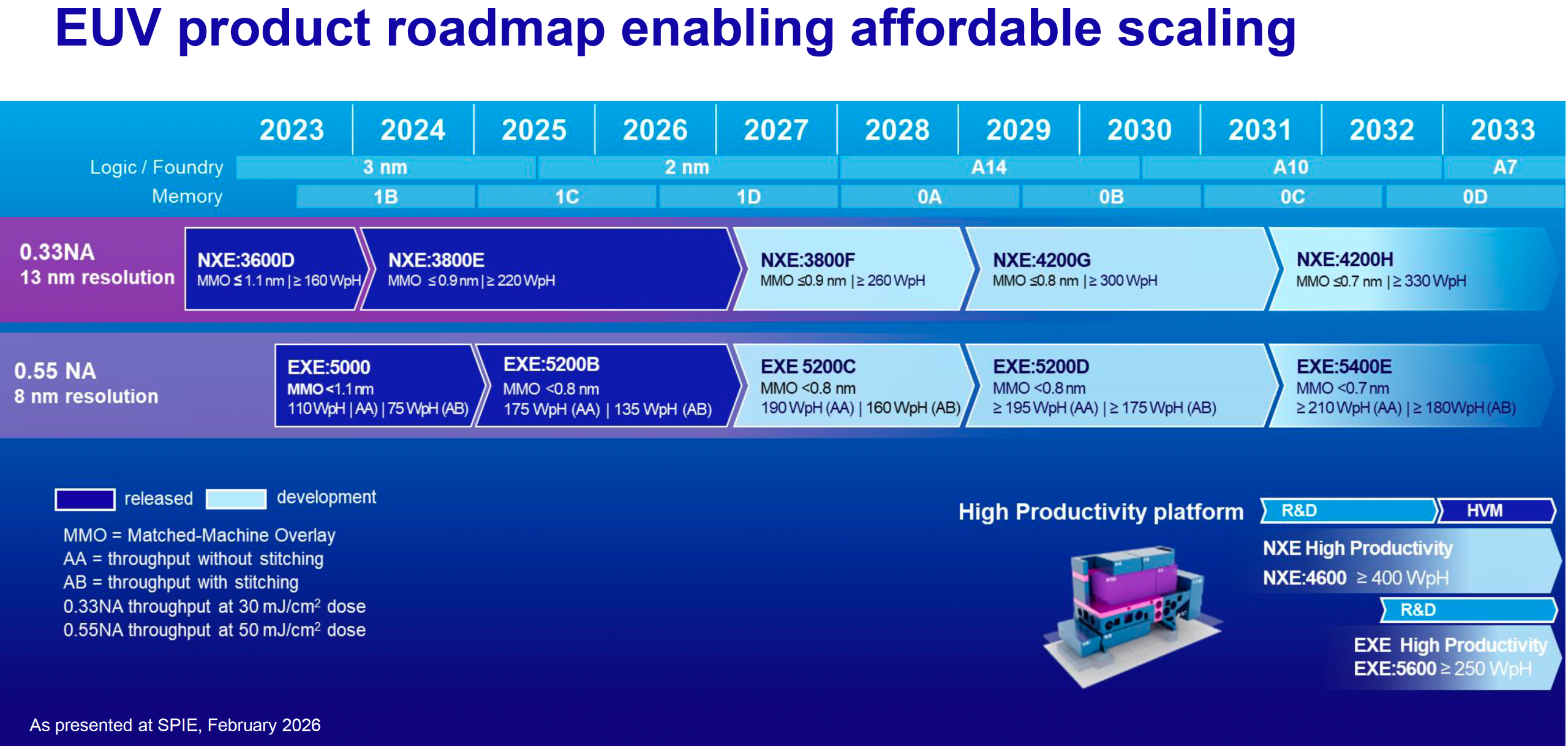
High-NA EUV lithography is a major step forward from today's Low-NA EUV tools. With a numerical aperture of 0.55, High-NA systems can achieve an 8nm single-exposure resolution, compared with 13nm for 0.33-NA EUV scanners. The higher resolution enables chipmakers to pattern smaller, denser features in a single exposure, replacing complex Low-NA EUV multipatterning schemes with a single High-NA exposure. This can reduce the number of masks and process steps, shorten manufacturing cycle times, and potentially improve pattern fidelity and yields, especially on critical layers of next-generation process technologies.
However, this improvement comes with a significant tradeoff. Conventional 0.33-NA EUV uses 4X reduction optics in both directions, which enables a 26×33 mm exposure field with standard 6×6-inch photomasks. By contrast, High-NA EUV uses 4X/8X anamorphic optics, so the same mask can only expose a 26×16.5 mm half-field, which is hardly a problem for client-oriented designs that are barely larger than 429 mm². However, large dies that fit within a conventional 26×33 mm EUV field must now be patterned using two High-NA exposures stitched together, or split into a multi-chiplet design.
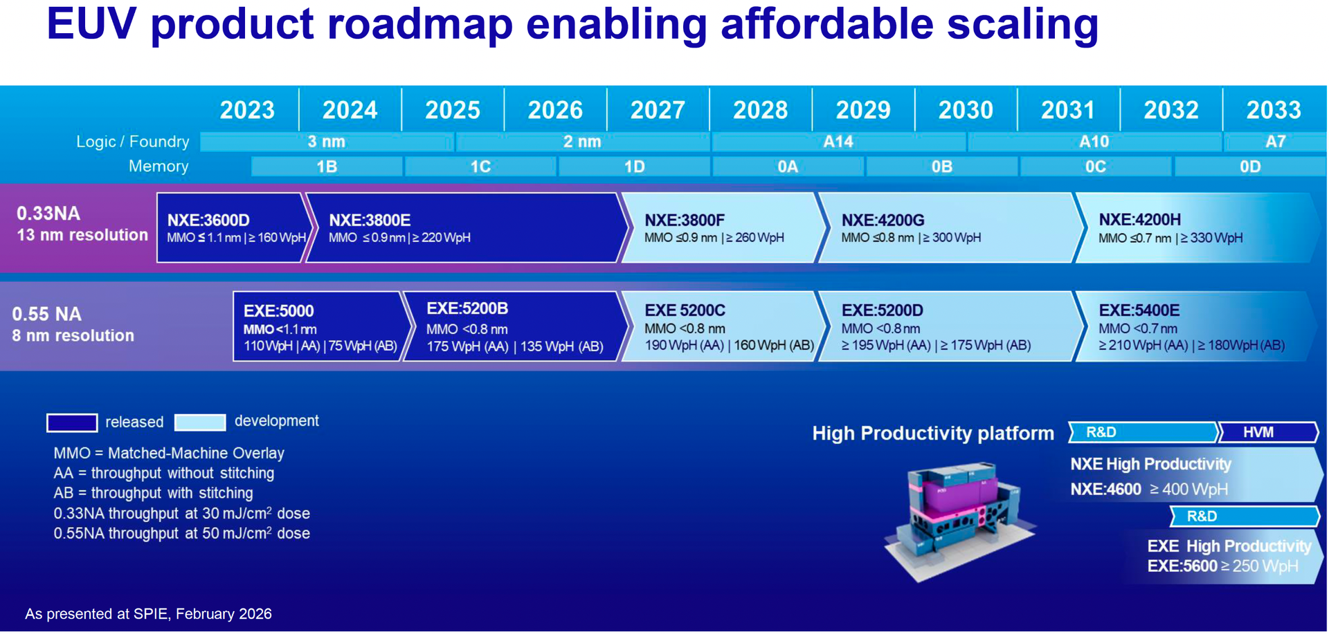
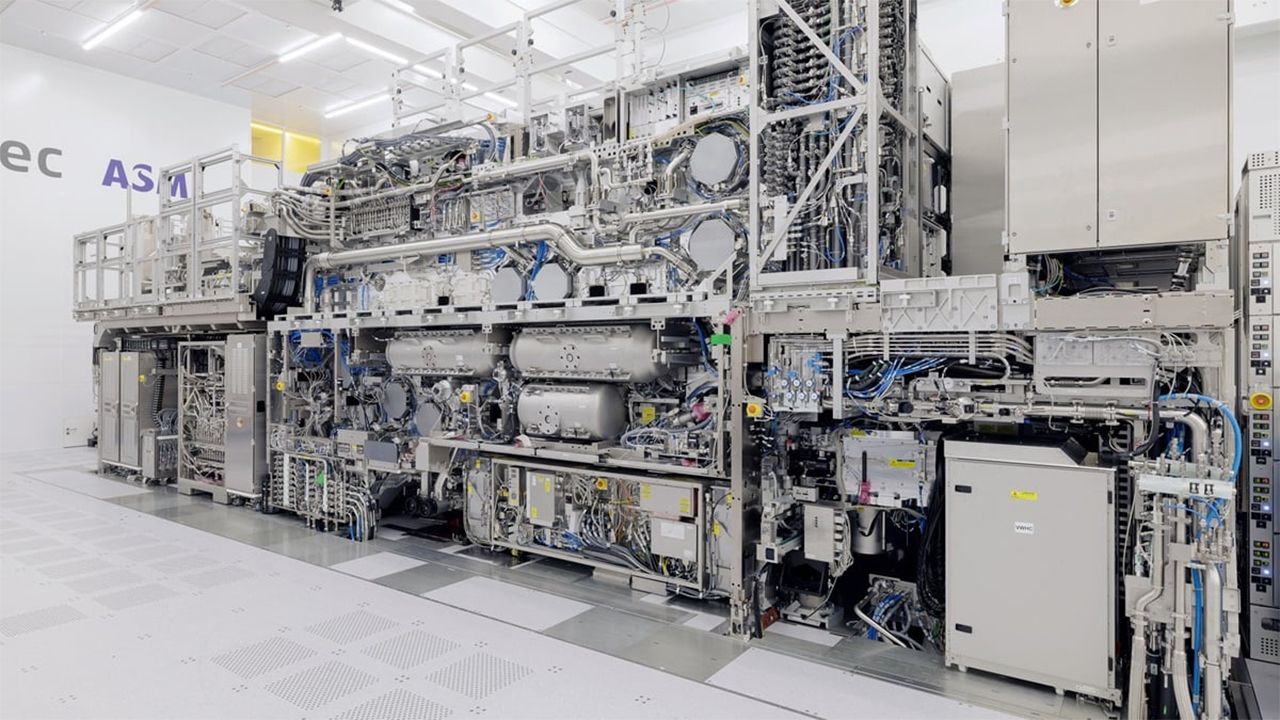
Stitching is a workable near-term solution that all chipmakers, including Intel, Samsung, and TSMC, use, but it comes with multiple drawbacks. First, it reduces the throughput of ASML's Twinscan EXE:5200B scanner from up to 175 wafers per hour for half-field exposures to around 125 wafers per hour when stitching is used. Secondly, chip designers must account for the stitching boundary, which means additional design rules and reduced floor planning freedom.
Finally, the two exposures must be aligned with extreme precision so that features crossing the boundary connect properly. Even tiny alignment errors can distort lines and vias, or compromise interconnects and thus potentially create defects and lower yields. Such yield loss is very expensive in the context of large CPUs and GPUs produced using Low-NA EUV systems. If yield is lost on more expensive High-NA EUV tools, the costs will be even higher, which greatly lowers the appeal of using these scanners.
New photomasks are needed
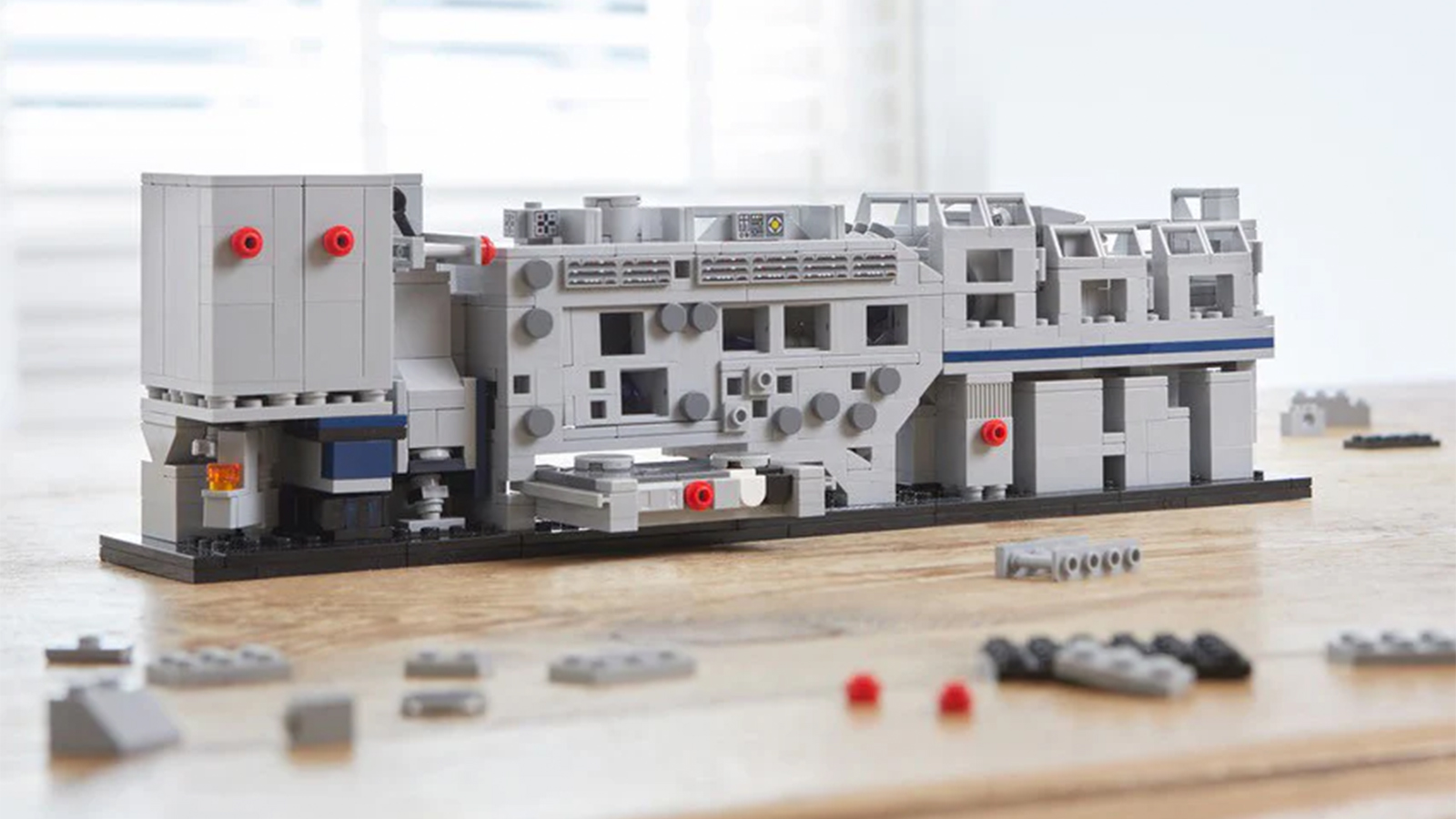
A Lego version of an ASML Lithography machine. (Image credit: ASML)
To eliminate the need for stitching, the industry is exploring larger orthogonal 6×12-inch photomasks to compensate for anamorphic optics. By doubling the reticle dimension corresponding to High-NA's 8X reduction direction, these masks are set to restore the traditional 26×33 mm full exposure field and enable even reticle-sized dies to be patterned without stitching.
However, 6×6-inch photomasks have been an industry standard for around three decades since the 1990s. Even the transition from DUV to EUV did not change the basic mask dimensions: EUV replaced transmissive masks with reflective multilayer masks but retained the 6×6-inch substrate form factor. As a result, the adoption of 6×12-inch reticles would require the industry to change the entire mask-making, mask handling, and lithography infrastructure built around the existing format.
Mask-blank suppliers like AGC and Hoya would need new or modified equipment to produce larger substrates and deposit uniform reflective EUV multilayers across a much larger area. Mask shops would need new or modified writers and etch tools to pattern the larger masks, as well as inspection and metrology systems capable of precise characterization of the new format. Cleaning equipment, pellicles, and pellicle-mounting devices would also require modifications.
The mask handling infrastructure would have to change as well. Suppliers would need larger mask pods, while fabs and mask shops would require compatible storage, transport, and automated handling systems. At the same time, they would have to retain support for existing 6×6-inch masks since existing and future Low-NA EUV and DUV scanners will continue to use the established format.
Perhaps the biggest changes would be required from ASML. Its High-NA EUV scanners would need modifications or a redesign to accept, clamp, move, and position the substantially larger reticles with the extreme precision required for EUV lithography.
Intel, Micron, Samsung, SK hynix, TSMC, and other chipmakers planning to adopt High-NA EUV lithography would then have to qualify the new masks, scanners, and other tools for their process flows and ensure that the full-field exposure capability works as intended.
As a result, the adoption of 6×12-inch masks would require a coordinated effort and significant investments from chipmakers, ASML, mask makers, and numerous equipment and materials suppliers.
To make matters more complicated, 6×12-inch masks will not replace the existing 6×6-inch format altogether, as noted above. The industry would therefore have to manufacture, inspect, transport, store, and handle two mask formats in parallel, which will add cost and complexity to an already expensive transition.
Timeline
The transition to 6×12-inch reticles is an industry effort currently supported by ASML, Intel, Samsung, and TSMC. It is going to take years and will happen well after High-NA EUV enters high-volume manufacturing with today's 6×6-inch photomasks, as the semiconductor industry prefers to adopt new technologies gradually.
Intel already uses High-NA EUV scanner(s) for select Intel 18A layers (patterned at Fab D1X) and supports both floorplanning within the half-field and stitching; Samsung plans to introduce High-NA EUV into DRAM high-volume manufacturing by 2028, and TSMC intends to deploy the technology for advanced-node production starting in 2030. All three companies plan to start High-NA EUV adoption with 6×6-inch masks.
Intel seems to be leading the pack with 6×12-inch reticles as it has been working for three years to make them a reality, but the company remains tight-lipped about the timing of its adoption of the new photomasks. Meanwhile, the ASML-TSMC initiative targets a 6×12-inch photomask pilot line by 2031, which should provide the foundry with a platform to develop and qualify the new mask format and associated manufacturing infrastructure. The ultimate target is full lithography-system readiness for advanced-node production by 2033.
That said, 6×6-inch and 6×12-inch photomasks for High-NA EUV patterning will likely co-exist on the market at least for some time rather than undergo an abrupt transition. At the end of the day, square 6×6-inch reticles that enable High-NA EUV scanners to expose fields as large as 26×16.5 mm (or 429 mm²) should be sufficient for the vast majority of client processors produced in the coming years. Larger 6×12-inch masks will matter primarily for much bigger designs, such as high-end AI accelerators, data center CPUs, DPUs, high-end GPUs, and FPGAs, where the ability to expose a full 26×33 mm field without stitching becomes considerably more valuable.
For years, TSMC has tried to avoid making public comments about its plans to use EUV lithography with a 0.55 numerical aperture optics, or High-NA EUV, because the company's developers had a good idea how to keep advancing process technologies without using $400 million scanners. However, TSMC cannot rely on Low-NA EUV systems forever, so this week the company announced plans to use High-NA EUV starting from 2030.
TSMC did not formally reveal which fabrication technology will be the first to adopt High-NA EUV, though the year 2030 points to a few candidates. What TSMC did say is that it expects the number of layers processed using High-NA EUV to eventually increase as its fabrication technologies become more complex, driven by increasing complexity of transistor architectures, which is probably an implication for more sophisticated implementations of gate-all-around (GAA) transistors as well as complementary field-effect transistors (CFETs) later on.
TSMC plans to start using High-NA EUV lithography tools for high-volume manufacturing in 2030 using conventional 6×6-inch photomasks. The company then plans to build a pilot line that uses 6×12-inch photomasks in 2031 with the goal of bringing 6×12-inch High-NA lithography systems into advanced node production by 2033.
High-NA EUV lithography tools can achieve an 8nm single-exposure resolution, as opposed to a 13nm single-exposure resolution offered by today's Low-NA EUV litho systems. However, when used with conventional 6×6-inch photomasks, High-NA EUV scanners have only half the exposure field of their Low-NA counterparts, which creates challenges for manufacturing very large dies. As a result, chipmakers building massive AI accelerators must either stitch multiple exposure fields together or adopt multi-chiplet designs, two approaches that have their own other challenges, such as tool productivity and power consumption. To circumvent the 6×6-inch photomask limitations, TSMC is working with ASML to set the stage for 6×12-inch photomasks.
Changing the size of photomasks is not a trivial endeavor as it requires changing everything from EDA software to tools that produce and write masks as well as systems that handle them, which essentially means that the entire industry must work on this change. ASML seems to be optimistic about the transition as it is supported not only by Intel and TSMC, but also by Samsung.
"We expect the adoption of High NA EUV to increase progressively along the device scaling roadmap, first using current 6-inch masks and then further supported by 12-inch masks, which enable greater scanner productivity and allow the industry to meet the demand for smaller, faster and more energy-efficient chips," said Christophe Fouquet, president & CEO, ASML. "We are pleased by the strong initial support of semiconductor manufacturers, mask suppliers and partners for this initiative."
(Image credit: TSMC)
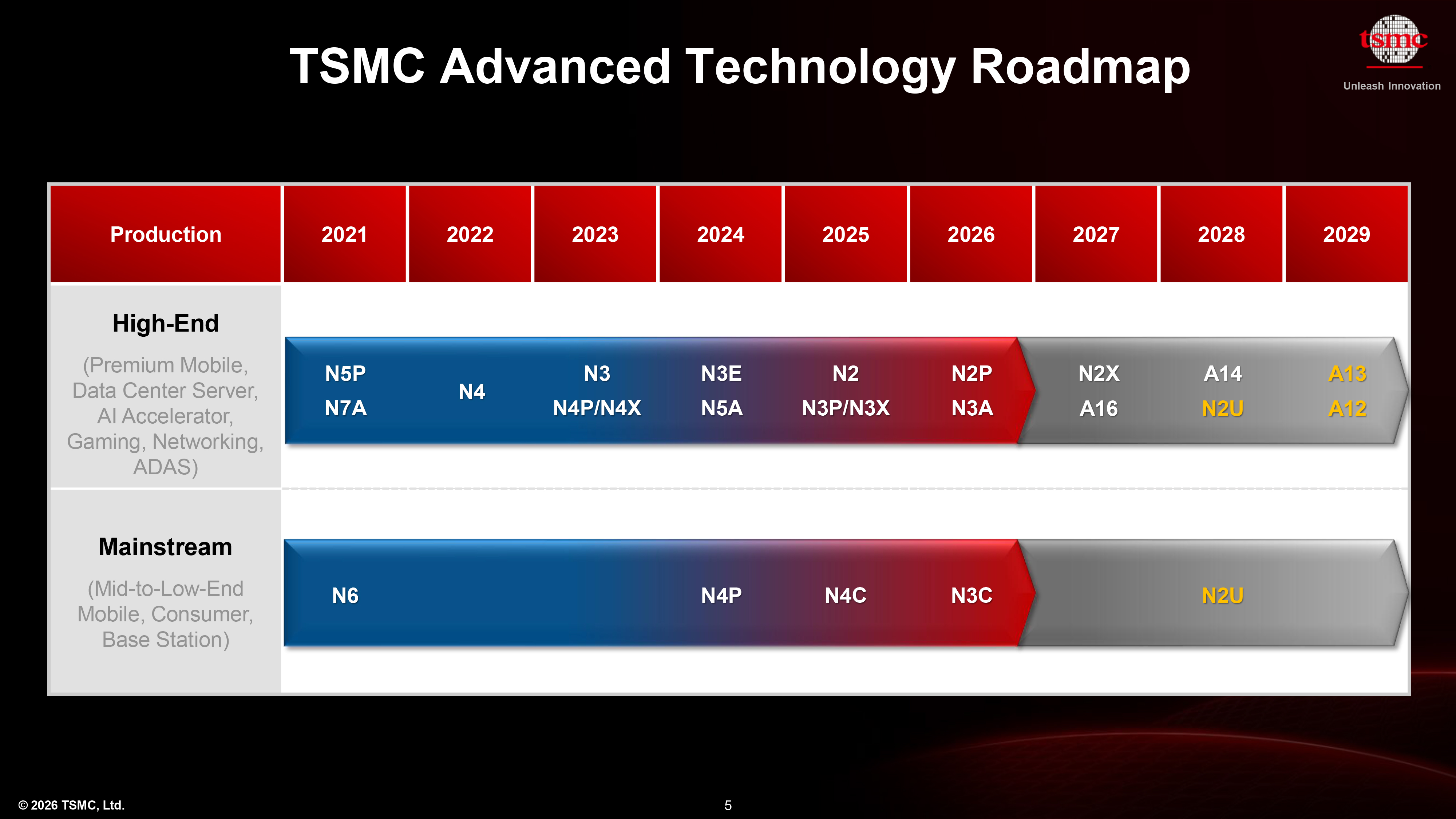
Perhaps the biggest intrigue about TSMC's usage of High-NA EUV lithography is which process technology will be the first to use the new systems. Based on what we know about TSMC's roadmap, A10 or A11 (1/1.1nm-class) seems to be by far the strongest candidates to use High-NA EUV scanners for the most critical layers. TSMC's latest strategy separates its roadmap into annual client-oriented nodes (N2, N2P, N2X, A14, A13) and roughly biennial high-performance nodes (A16 in 2027, then A12 in 2029). The company has already confirmed that A12 and A13, due in 2029, will continue to rely on conventional EUV lithography.
Since A13 is an optical shrink of A14 that increases transistor density by only 6%, with performance and power improvements yet to be disclosed, its successor in 2030 will likely have to deliver considerably more substantial gains. It is therefore reasonable to expect A13’s successor — whether it is called A11 or A10 — to adopt more advanced lithography and/or TSMC's 3rd Generation nanosheet GAA transistors to deliver significantly higher transistor density as well as meaningful performance and power improvements over its predecessor. Yet, we are of course speculating.
A 52-year-old Belgian-Chinese man has been arrested on suspicion of espionage for allegedly transferring specialized semiconductor intellectual property and trade secrets from Belgian chipmaker BelGaN, where he worked, to China. According to an AP News report citing details released by Belgium's federal prosecutor’s office on September 7, the Beijing-born Belgian resident was taken into custody on May 10 at a Brussels airport while attempting to board a flight to China.
The suspect — identified by Belgian media only as H.L. — previously held a senior research position at the now-defunct BelGaN, which specialized in gallium nitride (GaN) semiconductors. Investigators suspect he was concurrently leading a Chinese chip firm, GanKool, which was developing the exact same specialized gallium nitride chip technology as BelGaN. The company was established only a few months after H.L. joined BelGaN and was financed by a Chinese investment fund. The suspect now faces charges of industrial espionage, membership in a criminal organization, misuse of company assets, and unlawful disclosure of business secrets.
The espionage allegations emerged from an investigation into BelGaN's collapse. When the company collapsed into bankruptcy in the summer of 2024, Belgian authorities launched a routine financial probe into the failure. Investigators eventually uncovered highly unusual corporate activity. Instead of trying to keep BelGaN financially viable, the managers and the researcher may have actively tried to make the Belgian company “disappear” after transferring its proprietary knowledge. This led to further investigations that revealed GanKool’s existence and its connections to BelGaN.
In addition to the researcher’s role, the investigators also found evidence linking BelGaN's last CEO, a Chinese national, to the same Chinese rival. The prosecutors have said a second suspect remains at large, with Belgian media speculating that the CEO is the suspect.
The incident highlights the increasingly intense competition over technology and intellectual property in the semiconductor industry, particularly as China pushes to reduce its reliance on foreign chip technology while the U.S. continues to restrict its access to advanced processors and semiconductor manufacturing equipment. Just last month, South Korean court documents accused Chinese memory maker CXMT of using a detailed “Project Hefei” roadmap to obtain Samsung's proprietary DRAM technology, including a 620-step process recipe. A former Samsung engineer has already been sentenced to seven years in prison over the scheme.
Intel announced on Monday that it had processed more than one million 300-mm wafers using its High-NA EUV scanners, less than two and a half years after its first tool was assembled. For now, the company intends to use industry-standard 6-inch photomasks, which can expose 26×16.5 mm half-fields and therefore require field stitching for larger chips. However, Intel is also working on larger 6×12-inch photomasks that would enable High-NA EUV scanners to expose full 26×33 mm fields without stitching.
One million High-NA wafers
Intel's one million wafers figure includes wafers processed during tool installation and certification, R&D, and production. Earlier this year, Intel certified using High-NA EUV scanners for its 18A process technology, so right now these tools are used to make some of Intel's Panther Lake processors. Intel currently has two ASML Twinscan EXE:5000 tools and at least one EXE:5200B scanner. As of late February 2025, Intel processes around 30,000 wafers using its High-NA EUV tool, so going from 30,000 wafers by February 2025 to over a million by September 2026 is an enormous increase in cumulative High-NA utilization.
Since Intel's fleet expanded from two EXE:5000 systems to three and now includes the much faster EXE:5200B, the million-wafer milestone is really a fleet and process-maturity milestone that Intel has achieved first in the industry. What makes the company's milestone even more important is that ASML announced this April that all of the High-NA EUV scanners shipped by then processed over 500,000 wafers which achieving over 80% availability, which means that Intel has now processed more wafers using High-NA tools than the rest of the industry combined.
Sticking to stitching
Conventional 0.33-NA EUV has 4X magnification in both directions, enabling the familiar 26×33 mm exposure field with traditional 6-inch photomasks. However, 0.55-NA EUV uses anamorphic 4X/8X magnification, so the same 6×6 mask can provide only approximately 26×16.5 mm on the wafer. As a result, large dies that fit within a conventional 26 × 33 mm EUV field must be exposed as two half-fields using High-NA EUV, which is called stitching. While stitching is a workable near-term solution, it has several drawbacks.
(Image credit: ASML)
Firstly, it greatly reduces throughput from 175 wafers per hour to 125 wafers per hour on an EXE:5200B. Secondly, chip designs must account for stitching and must be developed with stitching in mind, which means less floor planning freedom. Thirdly, the two exposures must be aligned extremely precisely so that features crossing the stitching boundary connect properly. Even a tiny misalignment can distort lines and vias, or break interconnects, which potentially creates defects and reduces yields, which will be a particularly costly problem for large CPU and GPU dies.
6×12 mask effort progressing
To avoid using stitching, the industry — led by Intel — plans to shift to larger 6×12 masks, which will enable a 26×33 mm full field in one exposure. While this looks easy on paper, make the mask twice as long, changing the mask represents an enormous ecosystem change.
Moving from 6×6-inch to 6×12-inch photomasks would require substantial changes across the existing mask ecosystem, including mask blanks and deposition, etching, inspection and metrology, cleaning, pellicles, mask writers, and mask handling systems. Crucially, High-NA EUV scanners would also have to be modified or redesigned to accommodate the larger masks, which will make the transition a major retooling effort across the semiconductor supply chain. While neither ASML nor Intel confirmed that existing or planned High-NA EUV scanners can be modified to handle larger masks, all of the future High-NA EUV scanners to be launched before and after 2033 are designed around 6×6-inch reticles and stitching, according to ASML's roadmap.
It remains to be seen whether the industry moves on to larger 6×12-inch photomasks, but Intel appears to be the main evangelist for changing the mask standard that has defined projection lithography infrastructure for decades. If the effort comes to fruition, then Intel will likely have a considerable first-mover advantage over its industry peers because it will define and set the standard for the projection lithography industry for decades to come, an advantage that is hard to overestimate.
Being the world's largest contract chipmaker has its advantages for TSMC when it comes to negotiations with suppliers, as it naturally buys far more than others. However, it also has its difficulties because its requirements are dramatically larger than those of other foundries, and when they grow further, it gets exceedingly hard to source what it needs. Especially when its requirements increase nearly 2X in less than a year.
TSMC has nearly doubled its projected requirements for semiconductor production equipment since the end of last year as the foundry expands manufacturing capacity to address surging demand from the AI sector, said Cliff Hou, TSMC's deputy co-chief operating officer, during a fireside chat at Semicon Taiwan, reports FocusTaiwan. The world's largest foundry admits that it cannot meet all demand from all customers, though it is trying to catch up, according to Bloomberg.
TSMC makes projections about the number of tools it needs to purchase over the following year as well as its spending. After making that assessment late last year, the company discovered that by the end of the first quarter, the requirement had increased to 1.5 times that projection, and by July it had climbed to 1.9 times the original estimate, which means that TSMC's equipment needs had almost doubled in about six months.
TSMC itself attributes its increased needs to the number of new fabs that it is building in Taiwan and the U.S., though it should be noted that in addition to brand-new fabs, the company is also upgrading existing ones, which also need new machinery.
Interestingly, tool count does not seem to be proportional to tool cost. While TSMC increased its 2026 capital expenditure (CapEx) budget significantly in the recent eight months, it increased nowhere near 90%. Back in January, it guided 2026 CapEx to be from $52 billion to $56 billion. By April, it moved its estimate towards the high end of the original guidance, but in July it officially increased it to the range between $60 billion and $64 billion, or by around 15% if we only consider midpoints.
How exactly TSMC makes assessments about the number of tools it needs to buy the following year is something that remains to be seen, but perhaps a more pressing question for the industry is how it plans to acquire that equipment considering shortages of wafer fab tools due to massive demand from virtually all chipmakers.
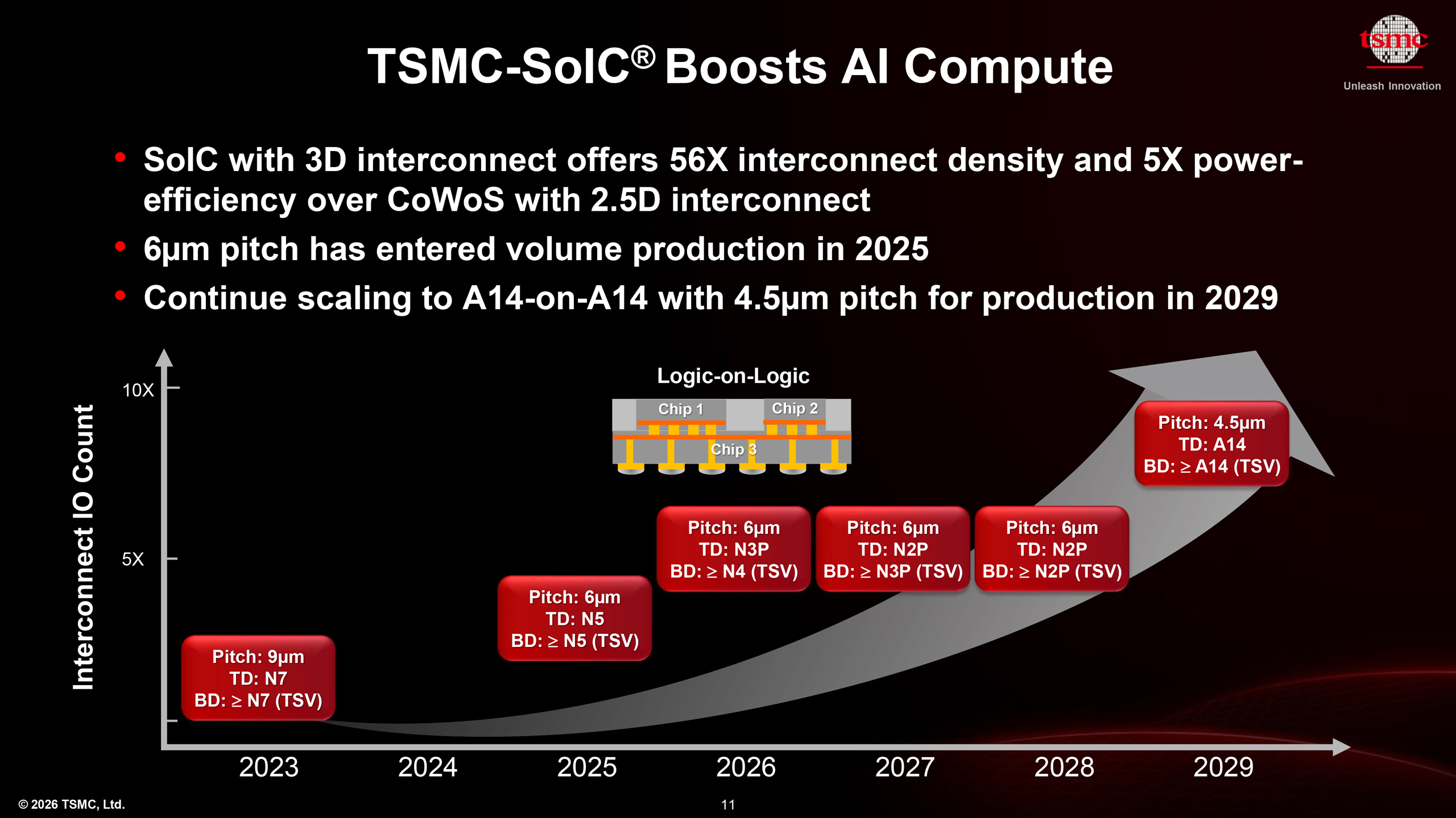
Hybrid bonding, the copper-to-copper joining technique that replaces solder microbumps in 3D chip stacks, is in high-volume production on logic chips and has just been postponed for use with memory. TSMC has scaled its SoIC bond pitch from 9 microns to 6 and laid out a path to 4.5 by 2029; Intel began shipping Foveros Direct hybrid bonding in its Clearwater Forest server CPU in the first half of 2026, and AMD has used the technology in volume since the first 3D V-Cache parts. However, a JEDEC decision earlier this year to raise the HBM stack-height limit lets HBM4 stay on the less sophisticated and expense microbump technology, deferring hybrid bonding's arrival in high-bandwidth memory, and is now set to debut in HBM4E and HBM5 at the end of the decade.
The technique works by polishing two dies flat, then bonding their copper pads and surrounding dielectric directly under heat and pressure, with no solder bump in between. Because there’s no bump to collapse, the connections can be packed far tighter. AMD has cited roughly 15 times the interconnect density of conventional 2.5D microbump stacking, and figures presented at TSMC's 2026 technology symposium put face-to-face hybrid bonding at around 14,000 signals per square millimeter against roughly 1,500 for face-to-back through-silicon-via stacking.
Wafer-to-wafer, die-to-wafer, and throughput
Microbumps have historically run at pitches around 40 microns, tightening toward 10 for the latest memory. Hybrid bonding, however, starts where microbumps end and keeps scaling: the leading edge is at 6 microns now, with 4.5- and 3-micron generations in development and sub-micron pitches demonstrated in research. Each step down multiplies the number of vertical connections between stacked dies, allowing a cache die or a compute tile to behave as if it were part of the chip rather than a separate component wired across a package.
The method is split into two different approaches: wafer-to-wafer and die-to-wafer. Wafer-to-wafer bonding joins two full patterned wafers face-to-face and dices them afterward, which allows the tightest pitch and fastest production because alignment happens once at the wafer scale. Imec and EV Group demonstrated a 200-nanometer wafer-to-wafer pitch with post-bond overlay below 40 nanometers at ECTC in May. The constraint here is that both wafers must carry identically sized dies, and every die gets bonded, including defective ones, so a single bad die on either wafer ruins the pair.
In contrast, die-to-wafer bonding places individual, pre-tested dies onto a wafer — which is what chiplet and HBM stacks require — because it allows known-good-die selection and the mixing of different die sizes and process nodes. There’s a penalty in terms of throughput with die-to-wafer as each die is picked, aligned, and placed in sequence rather than in one wafer-scale step.
The best die-to-wafer pitch shown at ECTC 2026, from CEA-Leti, was 1 micron, roughly five times looser than the wafer-to-wafer record. Because the dies are placed one at a time, the speed the bonder runs at sets the limit on how many chips it can produce. Applied Materials and Besi cite around 1,600 die placements per hour on the Kinex platform, and Besi's Chameo bonders are rated near 2,000 chips per hour, with the next generation aiming for 50-nanometer placement accuracy to reach finer pitches.
Hybrid bonding is difficult to achieve, as two surfaces have to be almost perfectly flat and clean. The dielectric holds on contact through van der Waals forces, so the polished surface can vary by no more than around 0.2 nanometers, and the copper pads have to sit a few nanometers below it, close enough that they swell into contact when the stack is heated to 200 to 300℃. A single particle smaller than a micron holds the surfaces apart and leaves a gap spanning many pads at once. So keeping the wafer clean and flat through the polishing step (known as chemical-mechanical planarization) is critical for good yields.
TSMC SoIC and Intel Foveros Direct
(Image credit: TSMC)
In terms of who’s leading hybrid bonding, TSMC’s System on Integrated Chips (SoIC) platform leads in terms of volume. At its 2026 North American Technology Symposium, the company laid out a pitch roadmap moving from 9 microns in 2023 to 6 microns in 2025 and 4.5 microns by 2029, with second-gen SoIC adding face-to-face bonding on top of the face-to-back stacking that the first generation supported. The node-stacking roadmap runs in parallel, from N3P-on-N4 today toward N2P-on-N2P by 2028 and A14-on-A14 by 2029.
With SoIC, the hybrid-bonded stack is built first as a vertical block, then placed into a CoWoS module alongside HBM on a silicon interposer, a combination the industry calls 3.5D. AMD's MI300 is the reference case, stacking compute and I/O dies by hybrid bonding before the assembly is mounted in CoWoS with its memory. SoIC handles the front-end vertical density; CoWoS handles the back-end lateral integration with memory.
Capacity is slowly growing, with TSMC building out its Chiayi AP7 site as its largest advanced-packaging campus. Output is targeted for 2026, and analysts at TrendForce have estimated SoIC capacity roughly doubling year on year from a few thousand wafers a month in 2024. Customers include AMD, whose 3D V-Cache and MI300 accelerators were the first volume SoIC products, and the Broadcom-built Fujitsu Monaka CPU.
Meanwhile, Intel's hybrid-bonding implementation, Foveros Direct, reached high volume with Clearwater Forest, the Xeon 6+ server processor built on the 18A node and demo’d at MWC back in March. The design uses a 9-micron copper-to-copper pitch to bond compute and I/O tiles onto base tiles that act as an active interposer, and Intel has described a second generation targeting a 3-micron pitch. Enabling that on a leading-edge logic node required a dedicated process variant, 18A-PT, which adds the through-silicon vias (TSVs) and bonding support that standard 18A doesn’t carry. The shift from Intel's earlier Foveros, which used solder microbumps across the Ponte Vecchio GPU's chiplets, to direct copper bonding is a generational change now playing out across its server offerings.
The unexpected HBM delay
(Image credit: Getty Images / Bloomberg)
The widely held assumption was that HBM, the stacked DRAM that sits beside every AI accelerator, would be hybrid bonding's largest market by volume. That changed back in January when JEDEC raised the HBM package height limit from 720 to 775 microns, and the extra room means 16-high HBM4 stacks can be assembled with microbumps after all. With HBM4 pad pitch at 10 microns, reporting from SemiEngineeringnoted that moving to hybrid bonding at that pitch wouldn’t yet make economic sense.
SK hynix has reflected that logic in its own planning, reportedly sticking with advanced mass-reflow molded underfill for 16-high HBM4 while keeping hybrid bonding as a backup and continuing to validate 12-high hybrid-bonded samples for later generations. The company demonstrated a 16-layer HBM4 sample at CES 2026, built without the all-hybrid bonding many expected the generation to require. The result pushes hybrid bonding's HBM debut toward HBM4E and HBM5, expected around 2027 to the end of the decade, where taller stacks and tighter pitches finally make the older bonding methods run out of room.
Meanwhile, the memory makers are building the packaging capacity regardless. SK hynix is investing $3.87 billion in an advanced-packaging plant in Indiana, with production targeted for 2028, and Micron broke ground on a $7 billion HBM advanced-packaging facility in Singapore early last year, with output expected around 2027. Those plants are sized for the volumes hybrid bonding will eventually carry, even as the first HBM4 generation ships on the older interconnect, meaning the equipment commitments are running ahead of the technology's confirmed deployment date in memory.
Samsung is doing the same thing from the memory side. Its SAINT packaging family includes SAINT-D, which stacks DRAM directly on a logic die, and the company has discussed a bufferless HBM4 design that removes the separate base die, with custom HBM logic dies reportedly moving to its 2nm foundry process for 2027 samples. At GTC in March, Samsung claimed hybrid bonding cuts thermal resistance by more than 20% against thermocompression bonding.
Another drag on the timeline is intellectual property. Adeia, which holds a large portfolio of bonding patents, sued AMD last year, alleging that the hybrid bonding behind 3D V-Cache infringes 10 of its patents.
China is pursuing the technique as a way around its lack of access to cutting-edge lithography. With SMIC limited to 14nm-class production and cut off from next-gen EUV, domestic researchers have identified 3D hybrid bonding as a route to competitive performance by stacking older logic and DRAM, with public claims of 14nm parts paired with domestic DRAM aimed at rivaling far newer GPUs. Given that it’s China we’re talking about here, those claims remain claims, and no foundry has demonstrated mass production of hybrid-bonded logic memory in China.
A scramble for tools
In terms of tooling, Applied Materials and Besi, partners on hybrid-bonding equipment since 2020, launched their Kinex die-to-wafer bonding system late last year, billed as the first fully integrated die-to-wafer hybrid bonder combining surface preparation, bonding, and metrology. Applied Materials has taken an equity stake in Besi, and reports from March placed Besi at the center of takeover interest from both Lam Research and Applied Materials, an indication of how important the bonding-tool market has become as logic adoption ramps and memory adoption is staged behind it.
Analyst tracking put Besi’s hybrid-bonding revenue on a path toward roughly €476 million by 2026, up from about €36 million in 2023, with second-half 2025 orders rising more than 60% against the first half on early HBM4 production-line bookings. Competing tool vendors are moving in alongside it: ASMPT has partnered with EV Group on hybrid bonding, and SK hynix is working with Hanwha Semitech on bonders targeting a commercial HBM launch in 2027. The sheer scale of this equipment build-out is a clear demonstration that the industry is treating hybrid bonding as an inevitability, even where the products that’ll use it are still years out.
Hybrid bonding is already in volume production, but its capability is outpacing its adoption. TSMC offers 6-micron pitch while its newest disclosed customer ships at 9; Intel ships at 9 with 3 on the roadmap; and the memory market that was meant to consume it in quantity has bought itself one more generation on microbumps. Two things will show where it goes next — whether any leading logic product drops below 9 microns in volume, and whether HBM4E marks hybrid bonding's first real use in memory before the end of the decade.
China's ability to produce lithography tools is comparable to that of market leader ASML sometime in 2004, an analyst with UBS wrote in a note to clients. The situation may change in the next two or five years when Chinese companies start producing immersion DUV lithography systems in mass quantities, and Chinese chipmakers begin to deploy them for production of actual chips. However, China's semiconductor industry will remain well behind Western industry. "They seem to be at a similar stage to ASML in 2004," wrote Francois-Xavier Bouvignies, an analyst with UBS, in a note for clients, reportsBloomberg.
For years, China's pursuit of semiconductor self-sufficiency stemmed from its ability to produce mainstream chips on trailing nodes using fairly advanced, though not the latest, tools from leading producers such as ASML, KLA, and Lam Research. In recent years, China found itself in a new reality in which it could no longer obtain the latest chipmaking tools and had to build them domestically. Although companies like ACM Research, AMEC, and Naura have developed world-class chemical wafer deposition, cleaning, etching, and oxidation/diffusion tools that are now mass-produced and used by Chinese chipmakers, none of the Chinese companies have managed to develop a competitive lithography machine that can be used to make chips on more or less modern nodes and initiate its mass production.
Photolithography is generally considered the most technologically complex and demanding individual process in advanced semiconductor manufacturing. Firstly, lithography systems themselves are extraordinarily complex and contain tens of thousands of individual components. Secondly, the required positional accuracy is extraordinary, as a modern lithography scanner needs excellent resolution, overlay, focus control, scanner-to-scanner matching, CD uniformity, and line edge roughness, just to name some of the requirements. Finally, a competitive litho system must guarantee predictable uptime, defect density, and performance. Perhaps the key thing here is that all of the required features must be achieved without compromises, as, for example, a machine with high resolution and ideal uniformity that can process one wafer per hour cannot be used for mass production.
Historically, over a dozen companies produced lithography tools. However, as they became more complex, only ASML, Canon, and Nikon survived, with ASML being the undisputed market leader and the only maker of EUV lithography scanners.
As China is essentially developing a parallel semiconductor ecosystem, there have been reports of multiple entities working on lithography systems, including Shanghai Micro Electronics Equipment (SMEE), AMIES (which seems to be a SMEE spin-off that includes Aishengna and Yuliangsheng units), SiCarrier (reportedly controlled by Huawei), and even Naura (which denies that it is developing litho tools). SMEE, which was established in 2002, is by far the most important established Chinese manufacturer of litho tools. Meanwhile, so far none of China-based makers of lithography have established mass production of immersion DUV scanners capable of producing chips at 45nm and below.
SMEE reportedly formally introduced its first immersion DUV lithography system called SSA/800-10W and capable of making chips on nodes down to 28nm back in 2023. However, there have been no evidence that SMEE has indeed started mass production of the SSA/800-10W and that it has been adopted by a single manufacturer for mass production of chips. While it is conceivable that not all chipmakers announce deployment of breakthrough tools, especially keeping in mind that Chinese vendors like SMEE have plenty of foreign suppliers, we would have seen at least some indirect evidence (starting from procurement/acceptance records as well as component orders all the way to job postings and scientific papers) that SMEE started shipments of the SSA/800-10W in 2023 – 2024 by now, assuming of course that there were any shipments.
Interestingly, but the reports about China-made immersion DUV scanners now mass-produced by Shanghai Aishengna Electronic Technology Group (a unit, or an affiliate of SMEE) re-emerged this July, again, without any evidence. This time around, the reports did not even mention targeted nodes or throughput capabilities. To make matters even more suspicious is the lack of reports about shipments of evaluation tools to chipmakers (like ASML does this with its High-NA EUV machines) as well as preliminary results of their process qualifications (like Intel does with ASML's High-NA EUV machines).
For a first-ever Chinese immersion scanner, it is reasonable to expect Chinese chipmakers to use it on engineering wafers, characterize it against ASML machines, develop recipes, identify drawbacks, and pass that information back to SMEE, something that should take about a year. Only once that first machine performs adequately does it make sense to order and qualify multiple SSA/800-10W units for mass production. In fact, such qualification will likely take another year for a single layer and more time for additional layers. To that end, an insertion of an all-new lithography scanner into an existing flow will take at least two years, but likely more. To that end, once SMEE (or its business units) and its customers figure out how the first Chinese immersion scanner should work, these scanners will still be far from mass deployment.
In any case, without any real indicators that Chinese makers of wafer fab tools can produce and ship immersion lithography scanners to customers, we can only state what the UBS analyst did: China's lithography industry is in a position where ASML was in the mid-2000s.
Samsung has unveiled a three-phase roadmap to progressively transform high-bandwidth memory (HBM) into an integrated memory-and-compute system, culminating in the company's zHBM architecture, which places the processor directly beneath the DRAM stack and eliminates the conventional 2.5D interposer link between the two. Detailing the roadmap at Hot Chips 2026, Samsung's Sangwook Han, of the company's DRAM design team, identified the base die as the key enabler of the evolution, which began with the company’s decision to manufacture the HBM base die on an advanced logic process.
In conventional HBM, the base die (B-die) was fabricated on the same DRAM process node as the core dies (C-dies) in the stack above. Starting with HBM4, Samsung moved the base die to a 4nm logic process, primarily to reduce power draw and minimize die area. Additionally, it gave Samsung a much more capable piece of silicon.
The company contends that a die built on the same class of logic process as XPUs could do much more than serve as a data interface. Samsung now plans to progressively offload more functions into the base die, eventually removing the physical gap between memory and the XPU entirely.
The current state of HBM and its growing constraints
The current HBM architecture comprises multiple DRAM core dies stacked vertically on a base die and connected through thousands of TSVs. The stack sits beside an XPU on an interposer, with the base die bridging the memory and compute silicon.
Bandwidth has been the main driver of HBM’s evolution. The current HBM4 stack has roughly 1 to 5 TB/s of bandwidth obtained through 1,000 to 2,000 I/Os running at about 8 to 16 Gbps each. These figures are expected to rise with upcoming HBM generations. The problem is that conventional ways of scaling bandwidth present significant challenges.
TSV signaling speed is difficult to increase, so HBM generations have added more TSVs instead. However, this consumes area and forces tighter TSV pitches. The PHY has also grown more demanding. HBM4 doubled the data I/O count from 1,024 to 2,048 DQs, and signaling speed keeps rising. Power is an even bigger issue. While energy per bit is improving, total HBM power continues to rise as bandwidth is scaling faster. Samsung says this is why HBM4 moves the base die to an advanced logic process, as the denser, more efficient logic reduces power draw.
This move underpins and enables the three-phase plan. An advanced logic node shrinks the interface circuitry while enabling the HBM base die to perform functions previously handled by the processor. Samsung calls this direction custom HBM, or cHBM, which keeps the conventional DRAM stack but customizes the logic underneath it for a specific accelerator.
(Image credit: Samsung)
Phase 1: Reclaim XPU area
The first phase is about handing processor area back to compute in what Samsung calls “XPU area reclamation.” AI accelerators are hitting familiar scaling walls, such as slowing process scaling and dies pressing against reticle and interposer limits. To expand compute, Samsung plans to evict non-compute blocks, moving their functions to the base die’s underutilized silicon.
The first target is the HBM Physical Interface (PHY), one of the largest blocks on the base die. Samsung proposes replacing the traditional interface with a much smaller die-to-die (D2D) link. On an 11 × 12.8mm HBM4 base die, the conventional PHY occupies more than 8 × 4mm, while the custom HBM D2D block is about 8.5 × 1.5mm, with channel depth cut from 5.5mm to 2mm. Because the matching interface on the XPU shrinks too, Samsung also reclaims processor silicon.
(Image credit: Samsung)
Conversely, shrinking the same power into less silicon increases power density and creates hotspots. Samsung’s answer is a Heat Path Block (HPB) that provides an alternative route for heat to exit the concentrated interface region. The company says an HPB covering more than half of the PHY can slash peak temperature by more than 35%.
The bigger Phase 1 change is moving the memory controller from the XPU to the custom HBM base die. Han estimated controllers account for 5 to 10% of an XPU's area — space that, refilled with compute, could yield a 10–20% performance gain. Moving the controller next to memory also enables a new SRAM-based repair scheme in which failed C-die addresses can be redirected to SRAM on the base die, avoiding the need to sacrifice an entire spare row or column for a single defective cell.
Phase 2: Making the die a more useful smart memory subsystem
Even with the controller moved in, Samsung says a substantial portion of the base-die area remains unused. Phase 2 fills that space with more functions, first with some relatively straightforward additions. The company proposes SoC-like telemetry and reliability features, including thermal, voltage, process, and aging sensors, as well as more advanced self-test hardware.
It also wants to use the edge of the base die for direct memory expansion, arguing that capacity is becoming as important as bandwidth. Dedicated controllers and PHYs could connect a secondary tier of external memory directly to custom HBM, rather than going through conventional PCIe expansion. Han said that extra memory could be LPDDR or even HBM, offering higher bandwidth and lower latency than PCIe-based memory extension.
Last in Phase 2 is compute — right on the base die. Samsung wants to place selected processing elements (PEs) under the DRAM, offloading memory-bound work while compute-heavy operations remain on the GPU. It calls this broader 2.5D architecture advanced HBM (aHBM), citing benefits such as less traffic across the interposer and reduced latency and I/O power draw.
(Image credit: Samsung)
Phase 3: zHBM goes fully 3D, placing the processor underneath the memory
Phase 3 appears to be Samsung's most radical step, with the company halting HBM architecture optimization and rebuilding it instead. Introducing zHBM, Samsung's “ultimate solution” for maximizing bandwidth under future AI's brutal power limits.
The zHBM concept eliminates the conventional side-by-side arrangement of XPU and HBM across an interposer. Instead, the processor sits directly beneath the DRAM stack in a true 3D structure. This architecture allows Samsung to replace the large edge PHY with distributed I/Os spread across the die. Data no longer has to travel laterally across an interposer, thereby shortening the physical path and eliminating the need for conventional HBM PHY and D2D link interfaces.
(Image credit: Samsung)
Samsung says the biggest payoff is power. Its projections show zHBM cutting I/O power by around 70% compared with HBM5. In another example, Samsung models roughly 2.3X more DRAM bandwidth while reducing memory power by about 100W compared to a four-stack HBM4E system.
On the flip side, thermals are the obvious complication. Han said Samsung is targeting roughly four-high zHBM stacks, compared with the much taller 12-high or 16-high configurations possible with conventional HBM, specifically because of heat. Distributed I/O helps by spreading the circuitry rather than concentrating it into hotspots, but zHBM is a balancing act involving capacity, bandwidth, heat, and physical integration.
Manufacturing zHBM will also require advanced wafer-on-wafer bonding and hybrid copper bonding to meet the required I/O density, with a much tighter co-design process between the DRAM and SoC teams. Samsung did not provide a firm launch date or timeline for the phases. However, HBM4’s 4nm logic base die is the concrete starting point, while cHBM and aHBM are nearer-term extensions, with zHBM as the long-term endpoint.
A team of scientists in Germany and Japan has demonstrated a solid-state cooling system that uses heat to generate the mechanical work required for refrigeration, potentially opening a route to processors and data centers that recycle some of their own waste heat for cooling. Developed by researchers at the Karlsruhe Institute of Technology (KIT) and the University of Tsukuba, the system — detailed in Nature Energy on August 28 — replaces the electrically powered actuator normally required for elastocaloric cooling with a heat-responsive shape-memory alloy, allowing the cooling cycle to run from an external heat source rather than a motor.
The prototype combines two ultra-thin metal films that serve as an actuator and a refrigerant. A 22-micrometer titanium-nickel (TiNi) shape-memory film contracts when heated, converting thermal energy into mechanical motion. This motion stretches and releases a 26.5-micrometer titanium-nickel-iron (TiNiFe) refrigerant film, triggering a reversible phase transition that produces cooling. In laboratory tests, Joule heating the actuator to 86°C produced a 12.9 K temperature span across the refrigerant film — the difference between its hottest and coldest states during the cooling cycle — and a 4.0 K span across the assembled cooling device, measured between its hot and cold sides. When the researchers replaced the resistance heating with an external 130°C heat source, the prototype still maintained a 2.2 K device-level temperature span, demonstrating that an external thermal source could drive the cooling mechanism.
Conventional refrigeration and air conditioning systems mostly use vapor-compression cooling. A compressor raises the pressure and temperature of a refrigerant, which then dumps heat in a condenser before expanding and evaporating at low pressure to absorb heat from the space being cooled. The technology is mature and efficient, but requires an electrically driven compressor and relies on refrigerants with significant global warming potential.
Solid-state cooling moves heat without the conventional compressor-and-refrigerant loop. Thermoelectric coolers, for example, use electrical current to create a temperature difference across semiconductor materials and are already common in compact electronics. However, the researchers note that thermoelectric devices typically reach only 10% to 15% of the theoretical reversed-Carnot efficiency limit, roughly one-quarter that of modern vapor-compression systems.
Elastocaloric cooling takes a different route. Certain shape-memory alloys change crystal structure when mechanically loaded and unloaded. Applying stress induces a phase transition that releases latent heat and warms the material. Once that heat is rejected, releasing the load reverses the transition, causing the material to absorb heat and cool. The solid alloy effectively becomes the refrigerant.
The problem is that the material still has to be repeatedly stretched and released. Existing elastocaloric systems generally use motors, hydraulic systems, or electromechanical actuators to provide the required force, adding electrical consumption, bulk, and mechanical complexity — particularly troublesome for miniature coolers. Instead, the KIT-Tsukuba team made one shape-memory alloy drive another. Heating the TiNi actuator film causes it to recover its original shape and contract. Mechanically coupled to the TiNiFe refrigerant film, that contraction supplies the force required for the cooling cycle. As the actuator heats and cools, it loads and unloads the refrigerant without an electric motor.
Broken down further, the system works as follows: the researchers take a shape-memory alloy (TiNiFe refrigerant film) that cools when released after being stretched. Instead of using a mechanical system to repeatedly stretch and release that alloy, they use another shape-memory alloy (TiNi) that contracts when heated and mechanically couple it to its cooling counterpart. When the TiNi is heated, it contracts, stretching and “loading” the refrigerant film. Once the heat is removed, the TiNi relaxes, releasing the film and triggering the phase transition that causes it to cool. Under cyclic heating, the TiNi alloy therefore provides the repeated stretching and releasing motion the TiNiFe requires for elastocaloric cooling.
The thermal actuator delivered a force-to-displacement ratio of 14.5 N/mm, compared with 1.1 N/mm for a commercial electromechanical actuator the researchers used as a reference. The thin films also provide a high surface-to-volume ratio for rapid heat transfer. Under Joule-heated actuation, the integrated device reached a steady 4.0 K temperature span after 20 cycles and a specific cooling power of 4.43 W/g. When driven from the external heat source, those figures fell to 2.2 K and 3.32 W/g, respectively.
This external-heat result is the real proof of concept. While the technology is still an early-stage laboratory experiment, a scaled, perfected version could have interesting implications. Typically, the heat the system needs to operate is generated from electricity or another form of energy. However, an ideal scenario would be to repurpose existing waste heat — a setup already attainable in data centers. Therefore, the technology has the potential to cool processors using the heat they generate!
However, applying it as a data center cooling technology is far from the technology's current state. The prototype produced just 2.09 milliwatts of cooling power at zero temperature lift. That is nowhere near the heat loads of modern processors, much less AI accelerators or data-center racks. The researchers also cite relatively slow actuation, limited strain rate, and the current heat-exchanger geometry among the factors constraining performance. There also needs to be a way to make the heating cyclical.
The team is now working to connect multiple films in parallel to increase cooling capacity. Further progress will require scaling the active material, improving heat transfer and operating frequency, and proving long-term durability. For now, the researchers have demonstrated the underlying energy chain in which heat can be converted into mechanical motion, and that motion can be turned into useful cooling without an electric motor driving the refrigeration cycle.
Intel's confidence in its 14A (1.4nm-class) fabrication process is rising as defect density drops. The company's own design teams are at work developing products that will use the technology, while external customers are now asking about 14A volumes Intel can get them, according to David Zinsner, chief financial officer of Intel, who spoke at Deustche Bank's 2026 Technology Conference. The CFO went as far as saying that 14A is Intel's best process since 22nm technology from the 2010's. But while the comment is optimistic, there is a caveat.
"When you look at the defect density, 14A is tracking better than the target curve we had for 14A," Zinsner said at Deutsche Bank's 2026 Technology Conference. "It is also doing better than any of the previous nodes in terms of how quickly we are bringing down the defects. In fact, we have not seen this performance since 22nm, which is arguably one of the best nodes Intel has ever put out."
Intel intends to begin risk production of its own products on 14A fabrication process in the second half of 2027 and then initiate its high-volume manufacturing in 2028, so 14A is two years away from mass production. So, what Intel's CFO said at the conference is that at this point in 14A's development, its defect reduction trajectory looks at least as healthy as the trajectory of the company's exceptionally successful 22nm process at a comparable point in its development (i.e., in 2010). There are a couple of catches with such phrasing, though. Firstly, the defect density on 14A now is not necessarily equivalent to a defect density on 22nm two years away from mass production. Secondly, due to advances of wafer processing and inspection equipment, what Intel counts as a defect now may not be the same thing as what it counted as a defect 16 years ago. Furthermore, defect density itself does not directly equal product yield.
Intel's 22nm was the company's first manufacturing process to rely on FinFET transistors and at the time was the most advanced process technology in the world; the rest of the industry moved to FinFET devices only with their 14nm and 16nm-class nodes in 2014 and 2015. By contrast, 14A will use second-generation gate-all-around (GAA) RibbonFET transistors, second-generation backside power delivery called PowerDirect, and will be able to use High-NA EUV lithography due to extremely complex patterning. Keeping all of that in mind, Intel's claim that 14A defect density reduction is progressing unusually well this far ahead of HVM is certainly good news.
Meanwhile, comparing 14A to 22nm's successors should be quite comforting for Intel as 14nm mass production was delayed by a year due to insufficient yield, the first-generation 10nm node was a failure, 20A was cancelled, 18A defect density was high even as it hit HVM milestone, while the company did not share almost any information about the progress of its Intel 4 and Intel 3 nodes.
There are good signs for 14A though: external customers are already developing products for this node, whereas the interest from external customers is now practical rather than theoretical.
"We are now seeing demand from our internal customers on 14A [and] they are actually probably the most cynical bunch out of anybody," Zinsner said. "The fact that they are now designing products on 14A was a good confidence boost for us as well. Then, engagements with customers externally, from a foundry perspective has significantly increased. Lip-Bu and the team are now meeting on weekly basis with customers. They are moving away from just looking at data to thinking about 'how much capacity can I get?' 'what does that supply look like?' So, we are now at a point where we have conviction around customers on 14A externally as well."
Intel initiated mass production of its 22nm-based Ivy Bridge processors in late 2011 and early 2012 and released them commercially in late April 2012. The product was highly successful (though overclockers did not like it because of inefficient thermal interface material between the die and integrated heatspreader), and 22nm fabrication technology served the company for many years, first for CPUs in 2012 through 2016, then for other products. Intel's 14A also promises to be a long-lasting node for Intel.
Glass-core substrates, the replacement for organic chip packaging that Intel promised in September 2023 with more than $1 billion behind it, are now in final qualification. However, the product is still not in a single commercial product. SKC, a material manufacturer and chemical affiliate of the SK Group, said on its July 27 earnings call that embedded glass substrate samples from its Absolics plant in Covington, Georgia, are undergoing package-level reliability evaluation in Taiwan, with results possible before year-end.
Samsung Electro-Mechanics formalized a 482.1 billion won ($310 million) glass-core joint venture with Sumitomo Chemical's Dongwoo Fine-Chem on July 2, targeting first production in the second half of 2027. Intel, which started the race, has shifted to licensing its patents and showing demo vehicles, with its own deployment now pointed at around 2030. However, and rather predictably, every timeline in the segment has slipped. Absolics originally planned mass production for the first half of 2024, and reported claims that AMD would adopt glass substrates for CPUs between 2025 and 2026 have come and gone unfulfilled.
Why glass?
The technical case for glass core substrates leans heavily on numbers Intel published a while back, such as 10 times the interconnect density of organic substrates and a 50% reduction in pattern distortion. Glass cores can be tuned to a thermal expansion coefficient of roughly 3 to 10 ppm per degree Celsius against silicon's 2.6, which cuts warpage by about half compared with organic cores, and rectangular panels in the emerging 510mm x 515mm format use more than 75% of their area for large die against roughly 50% for round 300mm wafers. Through-glass vias have been demonstrated at six microns in diameter with aspect ratios beyond 15:1 at ECTC 2025, and Georgia Tech has shown stacked glass running at 220 GHz with 0.3 dB of loss.
Glass also chips and cracks at the edges during drilling and dicing, and MIT Technology Review reported in March that early Absolics production runs broke hundreds of panels every couple of days during early testing days. Edge-coating work has cut measured edge stress from 95 MPa to 49 MPa, and low-temperature dielectrics that cure below 180°C have been developed to reduce thermal stress during build-up, but metallizing vias below 10 microns and holding nanometer-scale flatness across half-meter panels remain open manufacturing problems.
Intel's program
Intel demonstrated a working system booting Windows on a glass-core substrate in early 2025, and Rahul Manepalli, Intel's VP of module engineering, told MIT Technology Review that the benefits of glass cores are "undeniable" and that Intel wants "to be one of the first ones who do it." The commercial plan around that engineering has changed shape, however. DigiTimes reported in late July that Intel is in early-stage talks with Chinese cover-glass maker Lens Technology about a packaging partnership, but there has been no solid agreement made to date.
At NEPCON Japan in January, Intel Foundry showed its first thick-core glass substrate with two EMIB bridge dies embedded directly in the glass: a 78mm x 77mm package with two 800-micron-class glass layers, 10 redistribution layers on each side, and around 1,716 mm2 of silicon on top, roughly two full reticles, with no micro-cracking reported in testing.
There’s currently no production time to this, however, with TrendForce placing Intel’s commercialization somewhere around 2030, alongside co-packaged optics prototypes built on glass at its Rio Rancho, New Mexico site. Meanwhile, Amkor, Intel's packaging partner on the optics work, put commercialization within three years at an industry event in Seoul in April.
Korea aiming for 2027
Samsung Electro-Mechanics moved its glass program from advanced R&D into a business-execution unit in February and has been sampling from a pilot line at its Sejong plant since late 2024. The GLASEM joint venture announced on July 2 splits ownership: 66% to Samsung Electro-Mechanics and 34% to Dongwoo Fine-Chem, with site production in Pyeongtaek, and targets an operating plant in the second half of 2027, with the joint venture making the drilled and metallized glass core that feeds Samsung's substrate line. Korean industry reporting says samples have gone to AMD and Broadcom, and also puts Samsung's overall glass maturity at 40 out of 100, a gap between marketing dates and process readiness worth keeping in mind.
Absolics' $600 million plant in Covington, Georgia, backed by $75 million in CHIPS Act funding plus a further $100 million through the government's advanced packaging R&D program with Georgia Tech, has a Phase 1 capacity of 12,000 m2 of substrate per year, enough for roughly two to three million H100-sized packages. The company produced mass-production samples in the first quarter, began customer qualification that reportedly includes AMD and AWS, and is targeting mass production by the end of 2026. LG Innotek runs a third Korean program from its Gumi plant, with prototypes delivered in 2024 and production targeted for 2027 to 2028.
TSMC and Japan
TSMC's CoPoS line in Chiayi, built around 310mm x 310mm rectangular panels, received tools in February, completed its pilot line around June, and is aiming for pilot production in 2027, with mass production in the second half of 2028. Equipment supplier SCHMID has described glass integration in that platform as under review, not committed, and TrendForce puts TSMC's commercial-scale glass-core production after 2030, meaning that the industry's biggest packaging operation is going panel-level first and glass later, if at all. TSMC revived glass substrate research a couple of years ago after earlier deprioritizing it, reportedly under pressure from Nvidia, whose accelerator packages are the main thing outgrowing current packaging.
Japan’s Dai Nippon Printing began phased operation of a TGV glass-core pilot line at its Kuki plant in Saitama in December 2025 on 510mm x 515mm panels, with sample shipments from early 2026 and full mass production targeted for fiscal 2028. Toppan's pilot line for glass cores and interposers at its Ishikawa plant was scheduled for commissioning in July, and Nippon Electric Glass has scaled its ceramic-reinforced GC Core panel to 515mm x 510mm at 1mm thickness. Rapidus is studying panel-level packaging on 600mm x 600mm glass as part of its 2nm program, with viability put at the late 2020s. China has its own entrants, led by display maker BOE, whose pilot line is sampling.
TrendForce estimates Nvidia's Rubin Ultra package at roughly 7,470 mm2, about nine reticles' worth of silicon and memory, against around 2,739 mm2 for Blackwell, and CoWoS interposer wafers cost on the order of $10,000 each, comparable to a processed 7nm wafer.
Organic substrates warp and lose dimensional stability at those sizes, and round interposer wafers waste a growing share of their area, which is what glass panels are meant to fix. SEMI's first dedicated market report on glass cores, published in May with Global Net, projects initial production around 2028 in select high-performance applications and a 67.2% compound annual growth rate from 2028 to 2040, while Yole puts the advanced IC substrate market at $31 billion by 2030 with glass cores among the drivers.
At the moment, no production design exists, and all customers that have been named or otherwise attached to the tech, including AMD, Broadcom, AWS, and Nvidia, come from wider industry reporting. Nothing has been confirmed officially. As for whether we might see more substantial progress next year, Absolics will need to publish some solid package-level reliability results by the end of this year, or a first officially named customer at any of the Korean manufacturers. We also need to hear from TSMC on whether glass cores will go into CoPoS or remain under review into the 2030s.
 登录
登录