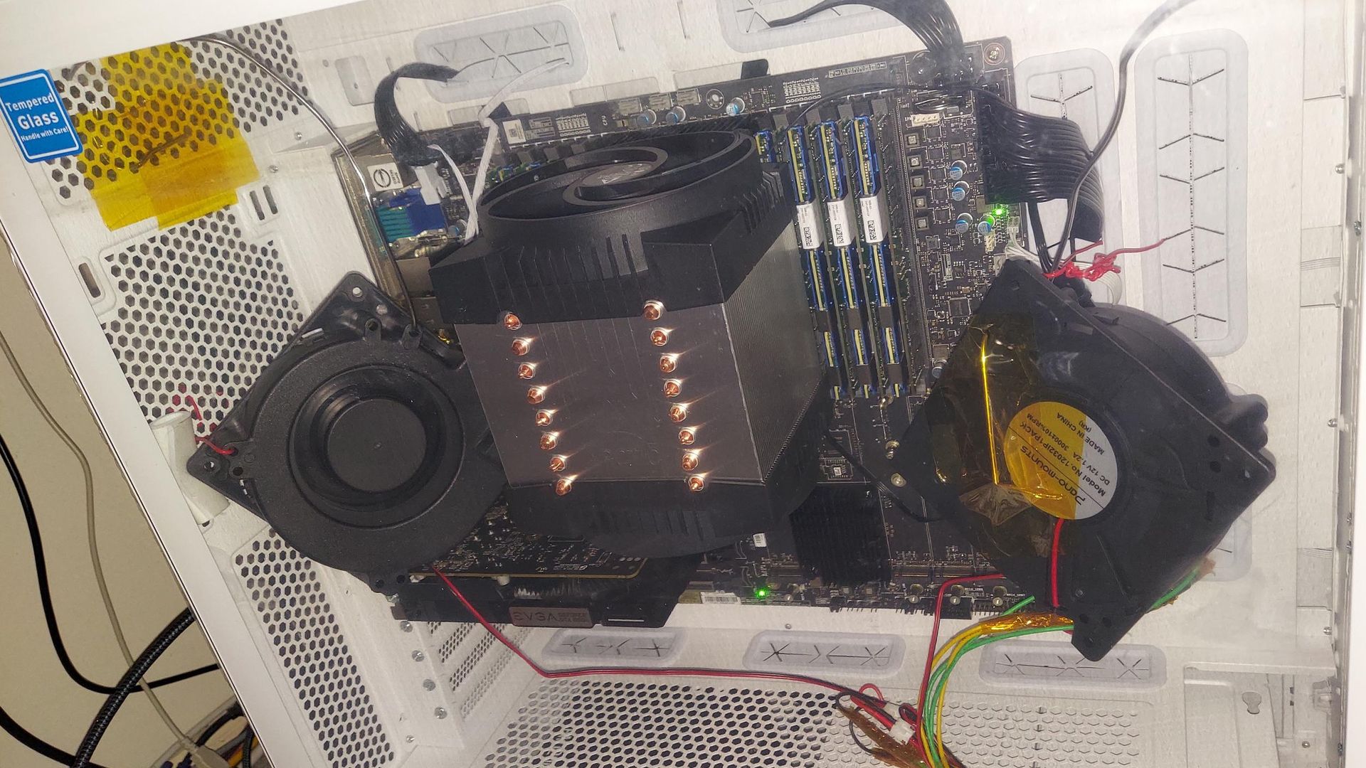
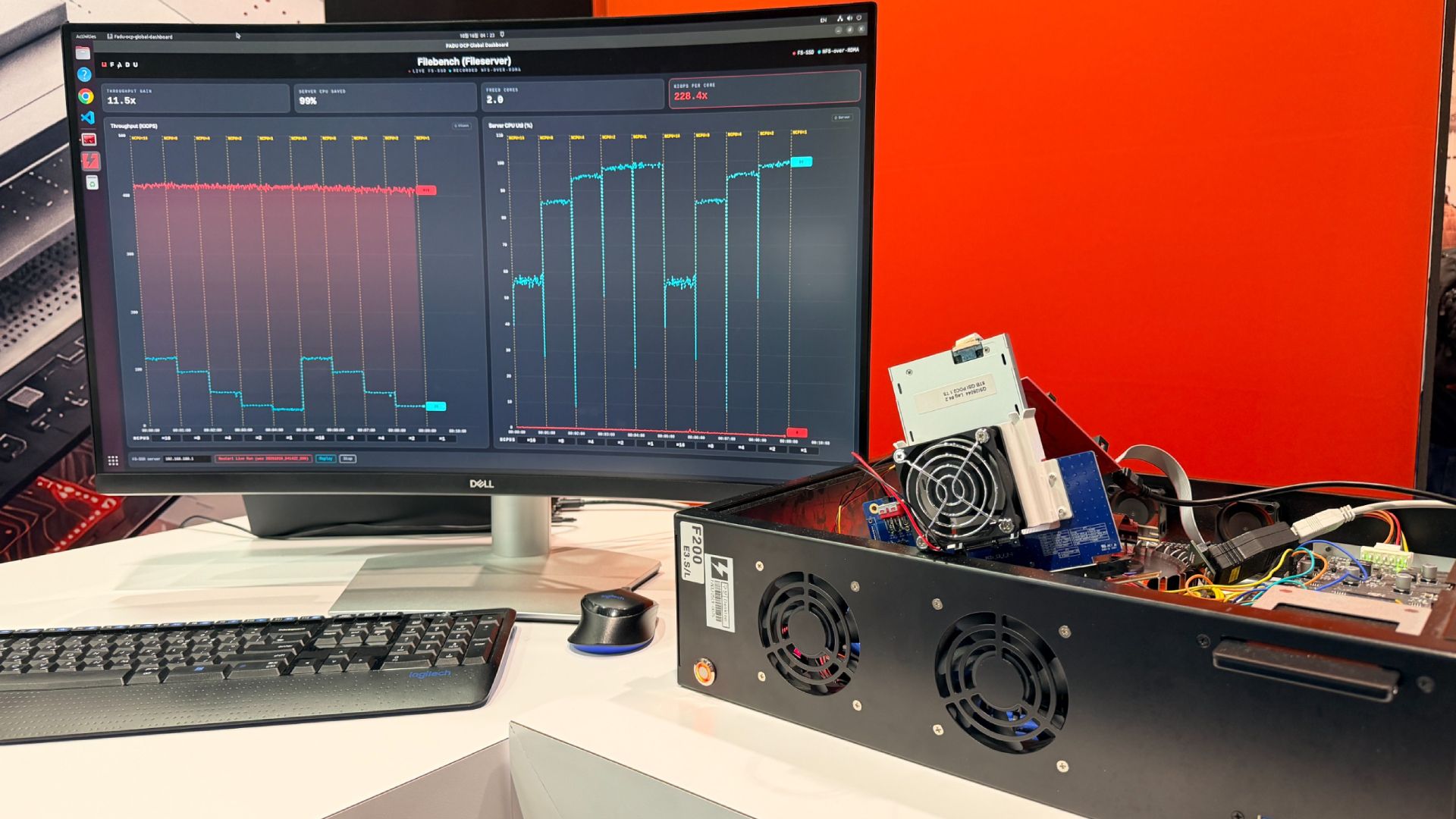
A homelab builder on Reddit has run Moonshot AI’s 2.8-trillion-parameter Kimi K3 AI model on discontinued second-gen Optane PMem 200 memory, using a 40-core 3rd-gen Xeon Scalable CPU and not a GPU for inference. The build runs hot, and the builder’s advice is that you “treat active DIMM cooling as mandatory,” with dual 12W blower fans aimed at the modules to get temperatures under control. The project, a follow-up to a separate user’s first-gen Optane build earlier this year, runs at a sluggish 0.85 tokens per second even with 1-bit quantization.
Kimi K3 is absolutely not built for home use, in our estimation, with Moonshot AI recommending data center inference engines to run it, and even the smallest community quantization needs at least 610GB of RAM. Using secondhand Optane, instead, is one of the few ways to reach that capacity at home. It doesn’t help that DRAM prices have skyrocketed, and the builder says the Optane memory costs “a fraction” of the equivalent.
Intel launched its Optane Persistent Memory 200 Series (PMem 200) in 2020 for its 3rd-gen Xeon Scalable CPUs in 128GB, 256GB, and 512GB capacities. On two-socket Xeon platforms, it runs at a higher effective MT/s rate than the first generation (PMem 100) that was used on the first project, and it can deliver an average of up to 32% more memory bandwidth. Optane can run in either Memory Mode or App Direct Mode; both builds had platforms allowing for each.
Memory Mode has the Optane act as system memory with DRAM as its cache, the method used in the first build, while App Direct exposes Optane as a separate, persistent region that the software maps directly, the mode used in the second. This can give “more control over where the model’s tensors live,” according to the first build’s creator, u/APFrisco, who planned to try it.
Performance does take a hit by going with Optane over DRAM, and with the higher 3-bit quantization, the speed went down even more to 0.75 tokens per second. One commenter points out that this is very slow, with a 50k-token task estimated to take 13 hours at about 1 token per second, but another notes that overnight batches don’t care as much about speed. Both speeds compare to the first build’s roughly 4 tokens per second, although in that case the builder had an RTX 3060 handling part of the model in addition to Memory Mode, a 2-bit quantization, and the smaller, earlier 1-trillion-parameter K2.5 model.
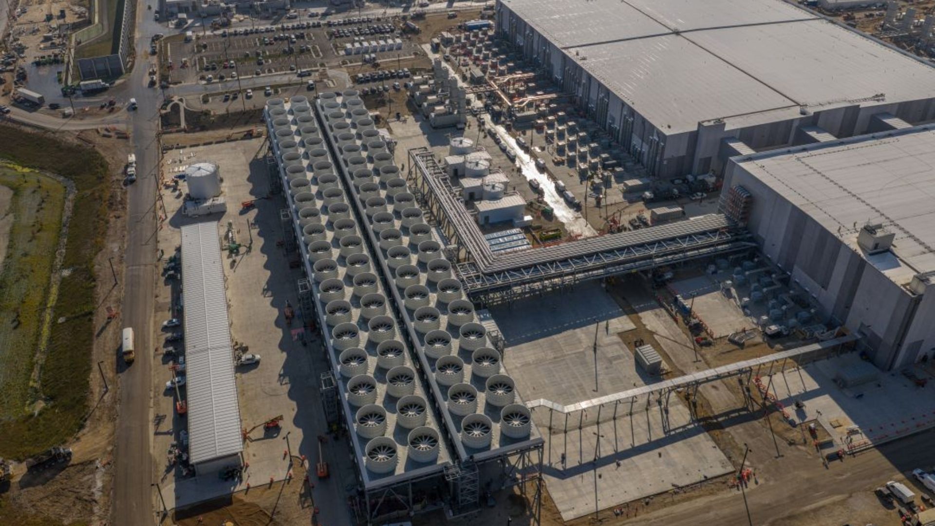
The latest builder also had to deal with heat output, with the Optane DIMMs getting “extremely hot” with sustained inference, creating a situation the builder says can endanger neighboring DRAM. That heat is consistent with Intel’s own specs, as the manufacturer rates the modules with forced airflow of 2.4 to 2.7 meters per second for cooling, which is what you expect to find in data centers. You might not normally have this level of airflow pointed directly at your memory sticks.
The expected operating conditions put each Optane module at 12W or 15W, regardless of capacity. If the build used four sticks, that would mean up to 60W of heat placed right next to the system memory. Throttling on these occurs at 83 degrees Celsius, with a thermal trip shutdown at 85 degrees, compared to the 85 degrees Celsius and up to 95 degrees in an extended range that typical DDR4 server memory is rated for. A lot of heat has to be removed from the system to keep things running.
The performance numbers given are pre-tuning — this means without tuning thread counts or NUMA affinity — so there is room for improvement, and one commenter also asked about using Memory Mode with DRAM caching for the most-used experts. The builder plans to add GPUs and to also load parts of the model into DRAM as a faster tier alongside the Optane, with “more benchmarks to come.”
Every once in a while we get a drive that comes across our desk that stands out, for good or for bad. The TeamGroup GA Pro falls into the latter category, enough so that we re-checked our results and contacted the company. We’ve managed to mostly sort out what’s going on and, while this is not the worst drive around, it has enough problems that we would generally not recommend it except if it's on steep sale.
TeamGroup’s array of storage offerings knows no bounds: if there’s a niche to cover, it makes an attempt. The GA Pro feels like such a try, although we’re not completely sure where it fits into the mix. The company is still working to iron out the bugs, if it can, but the technology is old enough that we wouldn’t hold our breath. On paper, it’s a PCIe 5.0 drive with DRAM that should beat any PCIe 4.0 SSD, but we found it struggles to live up to its own class of drive. Bright points are few and far between, but at least we can say it’s not the worst drive we’ve seen. The edges are just rougher than usual.
TeamGroup GA Pro Specifications
Product
1TB
2TB
4TB
8TB
Pricing
N/A
$331.99
N/A
N/A
Form Factor
M.2 2280 (graphene heatsink)
M.2 2280 (graphene heatsink)
M.2 2280 (graphene heatsink)
M.2 2280 (AirFlow I heatsink)
Interface / Protocol
PCIe 5.0 x4 / NVMe 2.0
PCIe 5.0 x4 / NVMe 2.0
PCIe 5.0 x4 / NVMe 2.0
PCIe 5.0 x4 / NVMe 2.0
Controller
InnoGrit IG5666
InnoGrit IG5666
InnoGrit IG5666
InnoGrit IG5666
DRAM
Yes
2GB DDR4
Yes
Yes
Memory
YMTC 232-layer TLC
YMTC 232-layer TLC
YMTC 232-layer TLC
YMTC 232-layer TLC
Sequential Read
10,000 MB/s
10,000 MB/s
10,000 MB/s
10,000 MB/s
Sequential Write
8,500 MB/s
8,500 MB/s
8,500 MB/s
8,500 MB/s
Random Read
N/A
N/A
N/A
N/A
Random Write
N/A
N/A
N/A
N/A
Security
N/A
N/A
N/A
N/A
Endurance (TBW)
600TB
1,200TB
2,400TB
4,800TB
Part Number
TM8FFJ001T0C129
TM8FFJ002T0C129
TM8FFJ004T0C129
TM8FGL008TTC133
Height
3.9 mm (w/ graphene)
3.9 mm (w/ graphene)
3.9 mm (w/ graphene)
62.3 mm (w/ AirFlow I)
Warranty
5-Year
5-Year
5-Year
5-Year
The TeamGroup GA Pro is available in 1TB, 2TB, 4TB, and 8TB capacities, although we only have the 2TB showing up at $331.99 at retail right now. The 8TB will probably be hard to find at this point. The drive is rated for up to 10,000 / 8,500 MB/s for sequential reads and writes, with no IOPS rating, although a drive like this can achieve 1 million or more. It has the standard five-year warranty with up to 600 TB of writes per TB of capacity.
TeamGroup GA Pro Software and Accessories
TeamGroup has a number of downloads available for this range of drives, which is better than nothing. They do maintain firmware for their drives, and we made sure our test sample had the newest revision, 050g05E7. Also available is the SSD S.M.A.R.T. TOOL, which is their SSD toolbox with basic functions, such as health monitoring. For backup and cloning on Windows, we continue to recommend MultiDrive, which continues to be updated based on user feedback.
TeamGroup GA Pro: A Closer Look
Tom's HardwareTom's HardwareTom's Hardware
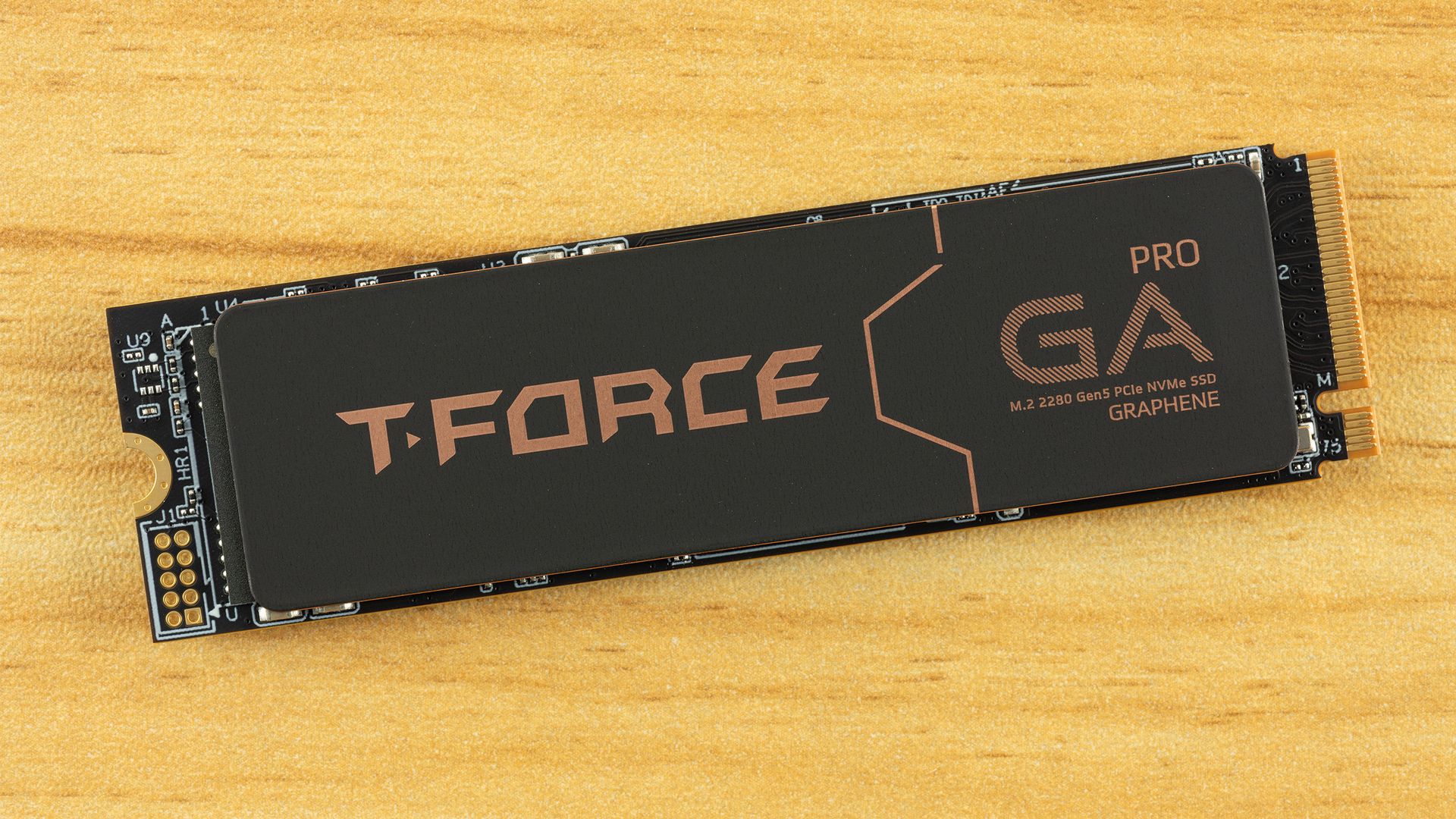
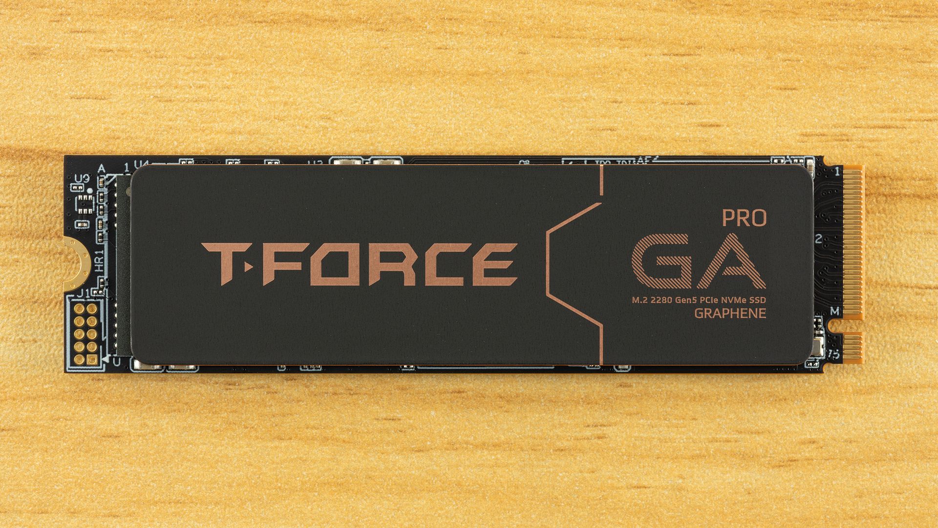
The good news is, the GA Pro has a graphene heat-spreading label. The bad news is, it’s insufficient to cool this drive. In most cases, you will want a heatsink on this. You can use a heatsink with the label in place, but you will have better luck if it’s removed. We are fond of graphene labels as they can be surprisingly effective, but it’s just not enough here.
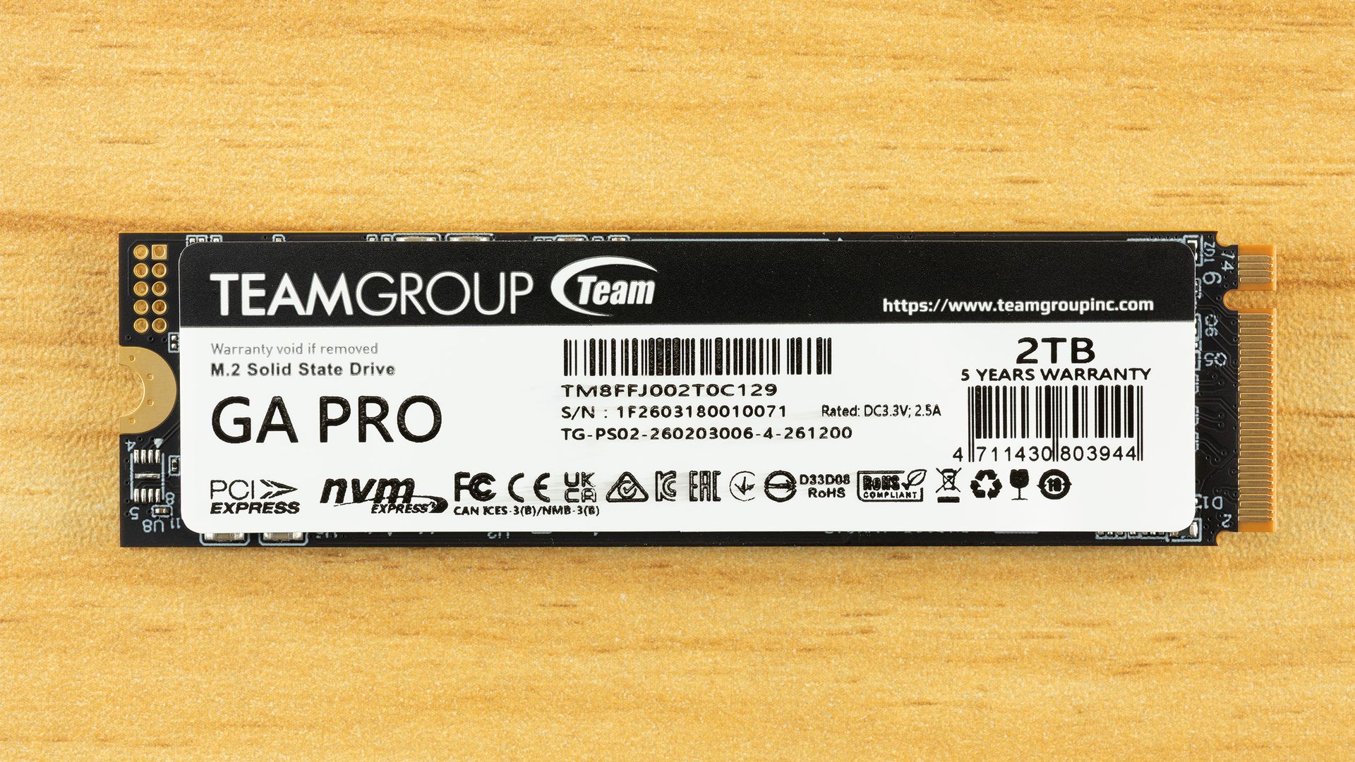
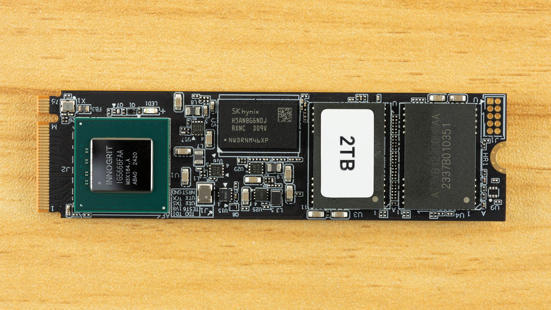
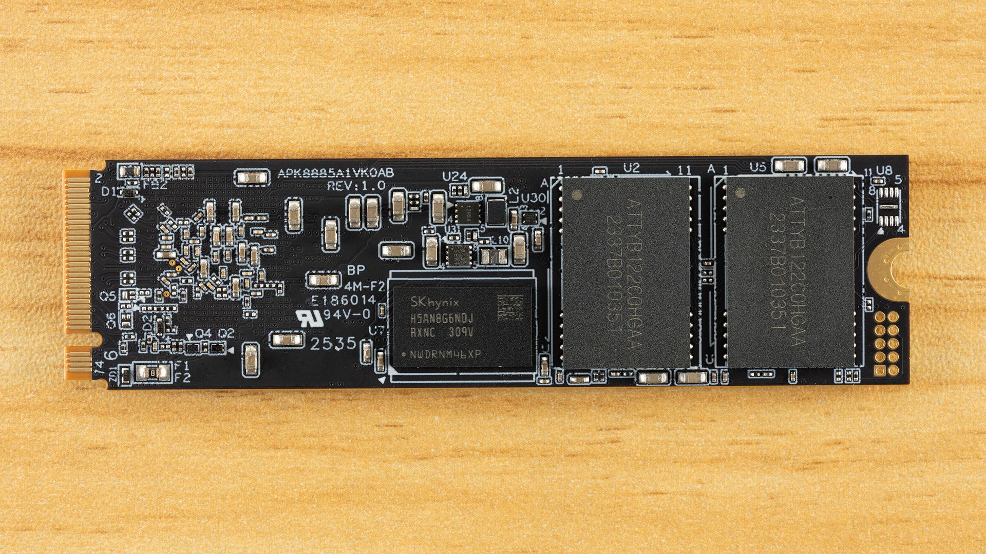
Then we have the label which, with the 3.3V / 2.5A rating, puts the drive at a very optimistic 8.25W. We measured over 12.5W peak in our testing below. We can’t go by reported power states, as these top off at 3.50 W. Since we can’t rely on that, we can’t say for sure what even the expected enter/exit latencies are, relevant given TeamGroup’s claims about the drive, which we’ll get to later. The drive is otherwise double-sided with a controller, two DRAM packages, and four NAND flash packages.
Tom's HardwareTom's HardwareTom's Hardware
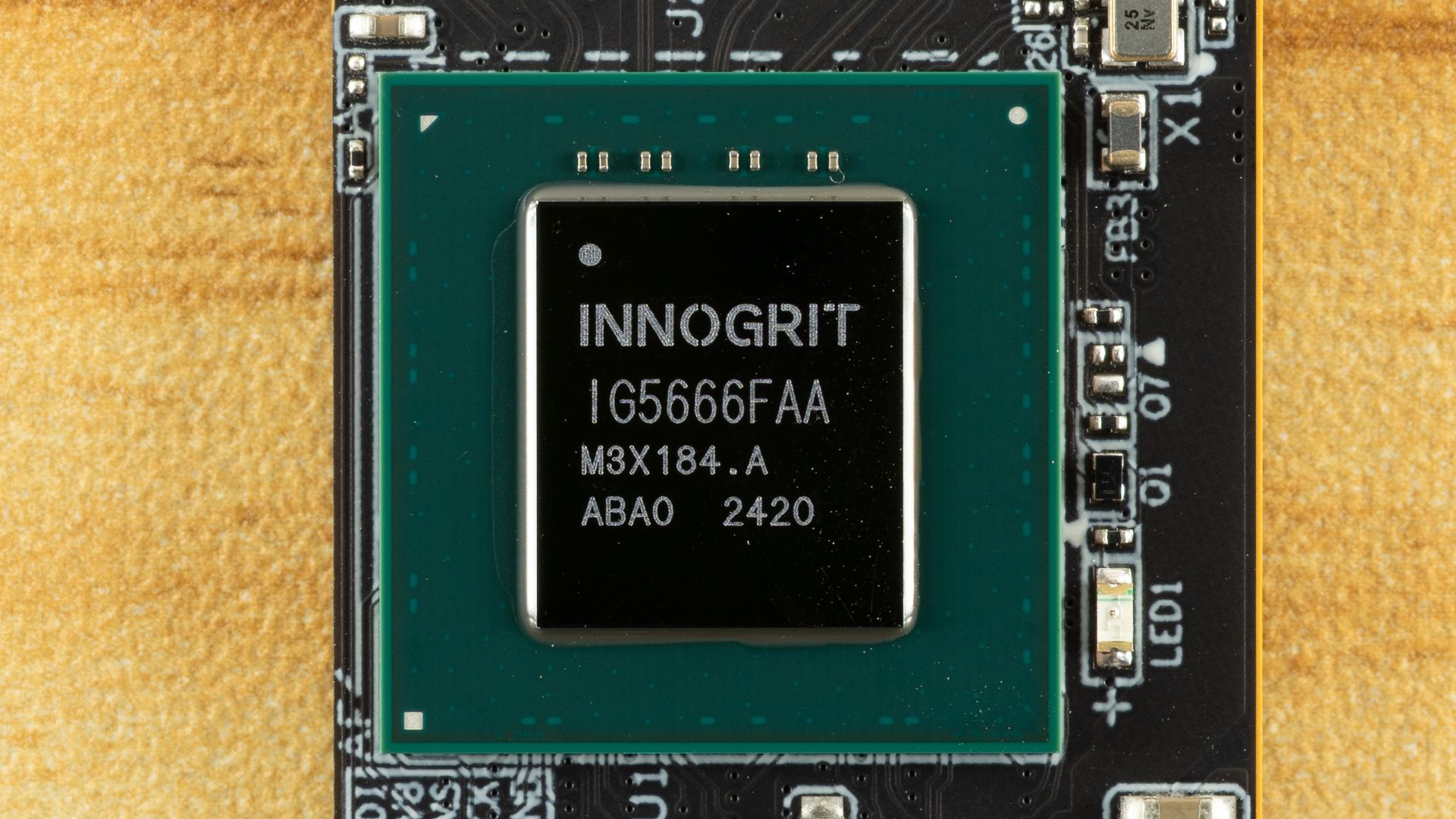
The SSD controller is InnoGrit’s IG5666, the company’s answer to the Phison E26 high-end PCIe 5.0 champion. We have better controllers in that segment now, like the E28 and SMI’s SM2508, but even at the time of release, the IG5666 was not very popular. Both the E26 and IG5666 run very hot due to using an older process node, and newer flash wasn’t available yet to more easily reach the bus speeds needed. The GA Pro is not running full-out but, to be honest, that doesn’t help much. Phison put a lot of work into getting the E26 up to full speed in steps, and even the base 10 GB/s ones run toasty.
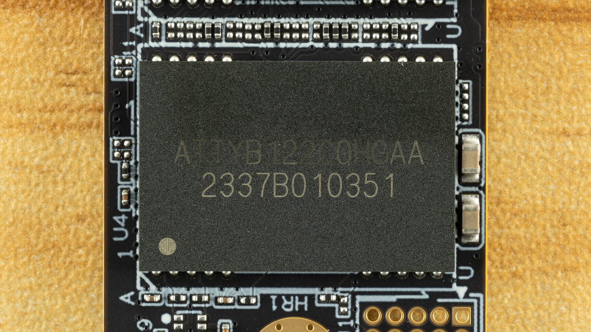
The drive does have the right amount of DDR4, 2GB, for this amount of flash. No problems there. The flash also looks to be YMTC’s 232-layer TLC, which is also perfectly fine. The controller is the weak spot here and, as we’ll find out, its firmware really keeps the GA Pro from reaching its full potential, even with its bandwidth cap.
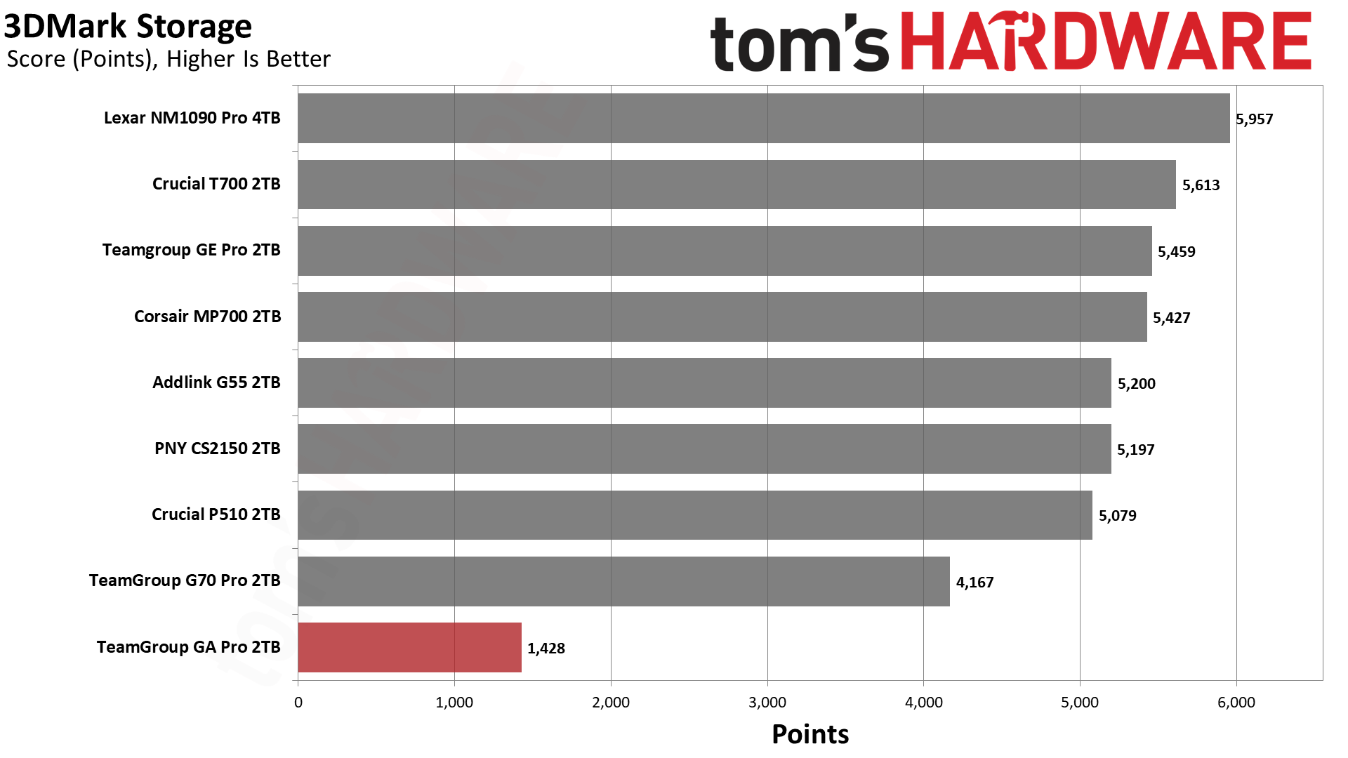
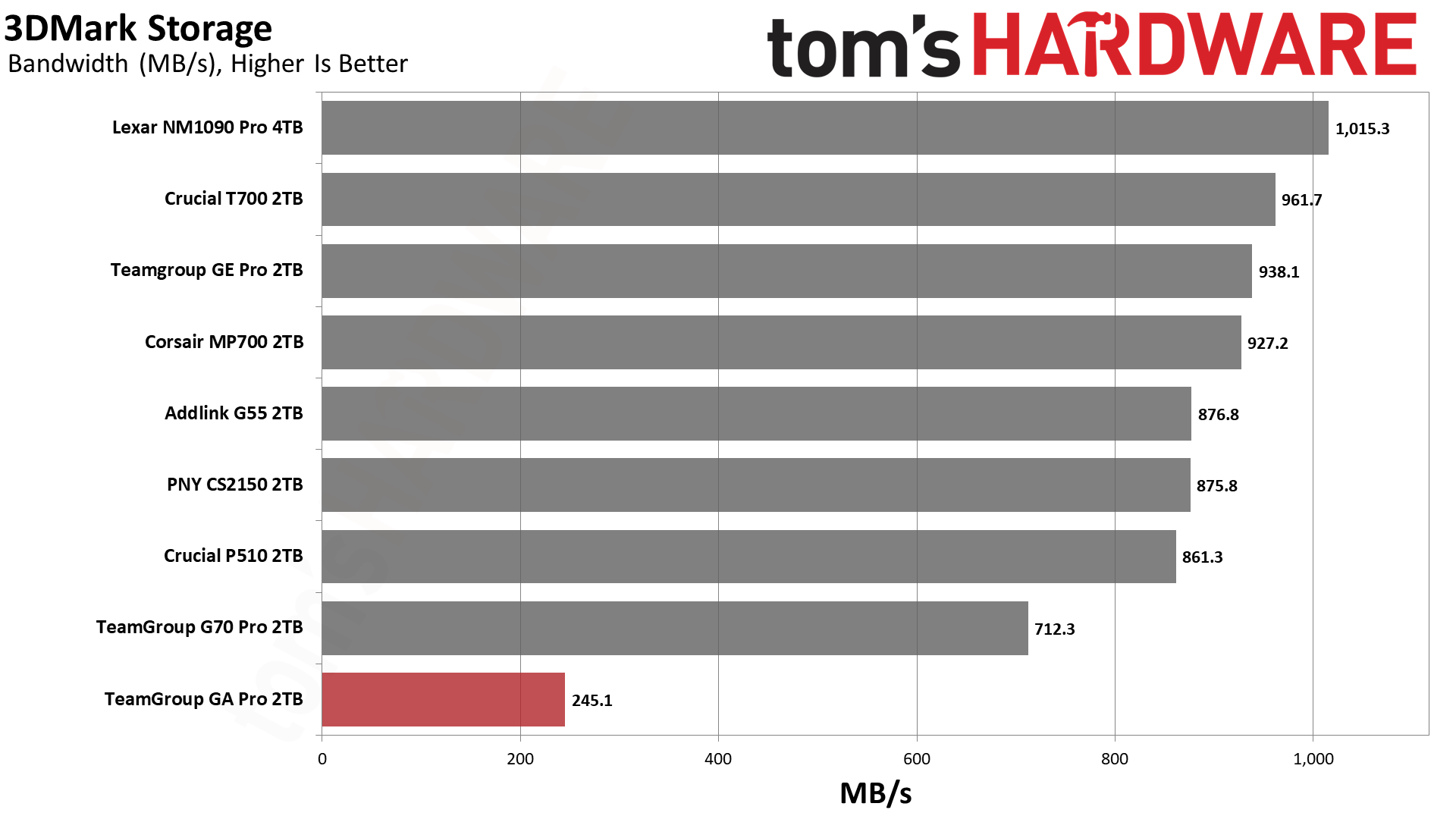
We’re throwing a mix of drives today at the GA Pro, in the interest of finding out why it performs the way it does. Direct competitors include the Crucial T700 and Corsair MP700, two Phison E26-based drives. The MP700 is rated at around the same speeds as the GA Pro, while the T700 is a step up, about halfway from there to the E26’s 14 GB/s effective ceiling. We also have the TeamGroup GE Pro sibling as a drive with similar hardware to the GA Pro but rated for the InnoGrit IG5666 controller’s full speed. The Addlink G55, PNY CS2150, and Crucial P510 also hover around the same specs but are later-arriving, DRAM-less drives. We also have the Lexar NM1090 Pro (4TB) in the mix as it’s a high-end PCIe 5.0 drive, but considered slightly more budget-leaning. Finally, the TeamGroup G70 Pro is our PCIe 4.0 stand-in for a last-gen comparison, from the same company and also with an InnoGrit controller.
Trace Testing — 3DMark Storage Benchmark
Built for gamers, 3DMark’s Storage Benchmark focuses on real-world gaming performance. Each round in this benchmark stresses storage based on gaming activities including loading games, saving progress, installing game files, and recording gameplay video streams. Future gaming benchmarks will be DirectStorage-inclusive and an evaluation for future-proofing is included where applicable.
Tom's HardwareTom's HardwareTom's Hardware
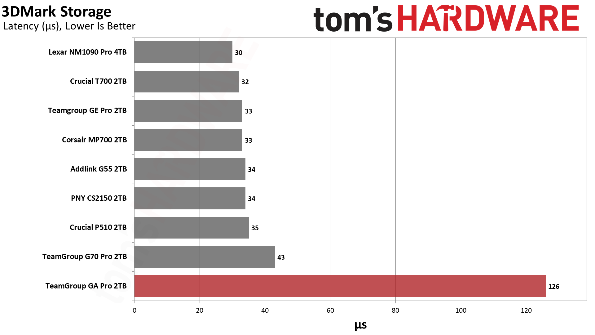
There’s no doubt about it; the GA Pro’s response here is quite poor. The drive’s score of 1,428 puts it pretty close to the SATA SSD range of around 1,000 to 1,400, and second to last of the 242 NVMe drives in our database. Now, this is plenty fast for gaming and much better than using an HDD, but it’s also terrible for an NVMe SSD, and we would not recommend it for this.
Right out of the gate, we began to question this drive’s results. We switched up our comparison drives, re-ran the tests, and ultimately contacted TeamGroup. In theory, this score is what we would expect given their explanation, which was that the drive was designed for CDM, ATTO, and sustained writes to get the most out of its bandwidth potential. The firmware being used drops the drive into a lower power state when the host is idle, and this can add unwanted command latency. That matches the 3DMark latency result.
Optimizing for certain workloads makes sense, but we don’t think this result is defensible. The likeliest reason for any such design, beyond the stated one, would be to handle heat. This controller runs hotter than any other PCIe 5.0 one we’ve tested. So, this is almost OEM-drive-like behavior, in the sense that it’s really trying to keep the drive within a certain envelope. We think the firmware is not operating as intended, but we at least accept the theory.
Trace Testing — PCMark 10 Storage Benchmark
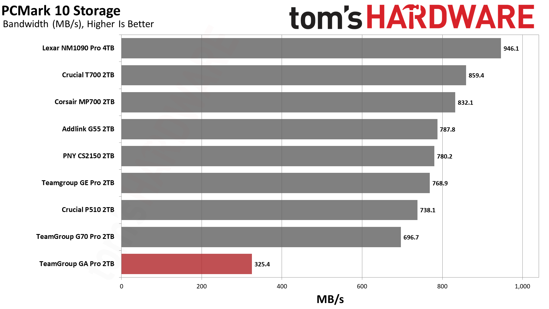
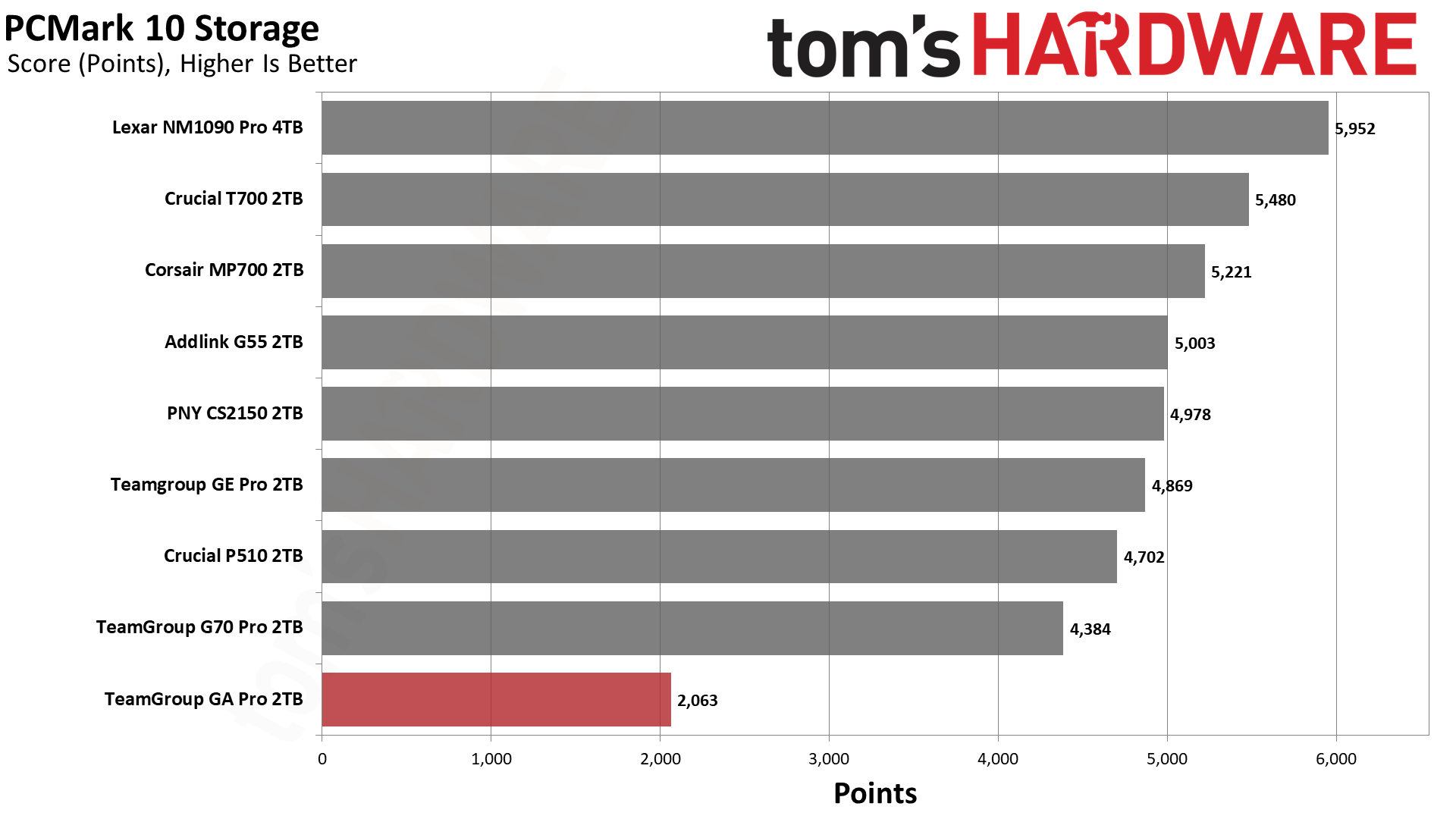
PCMark 10 is an industry standard trace-based benchmark that uses a wide-ranging set of real-world traces from popular applications and everyday tasks to measure the performance of storage devices. The results are particularly useful when analyzing drives for their use as primary/boot storage devices and in work environments.
Tom's HardwareTom's HardwareTom's Hardware
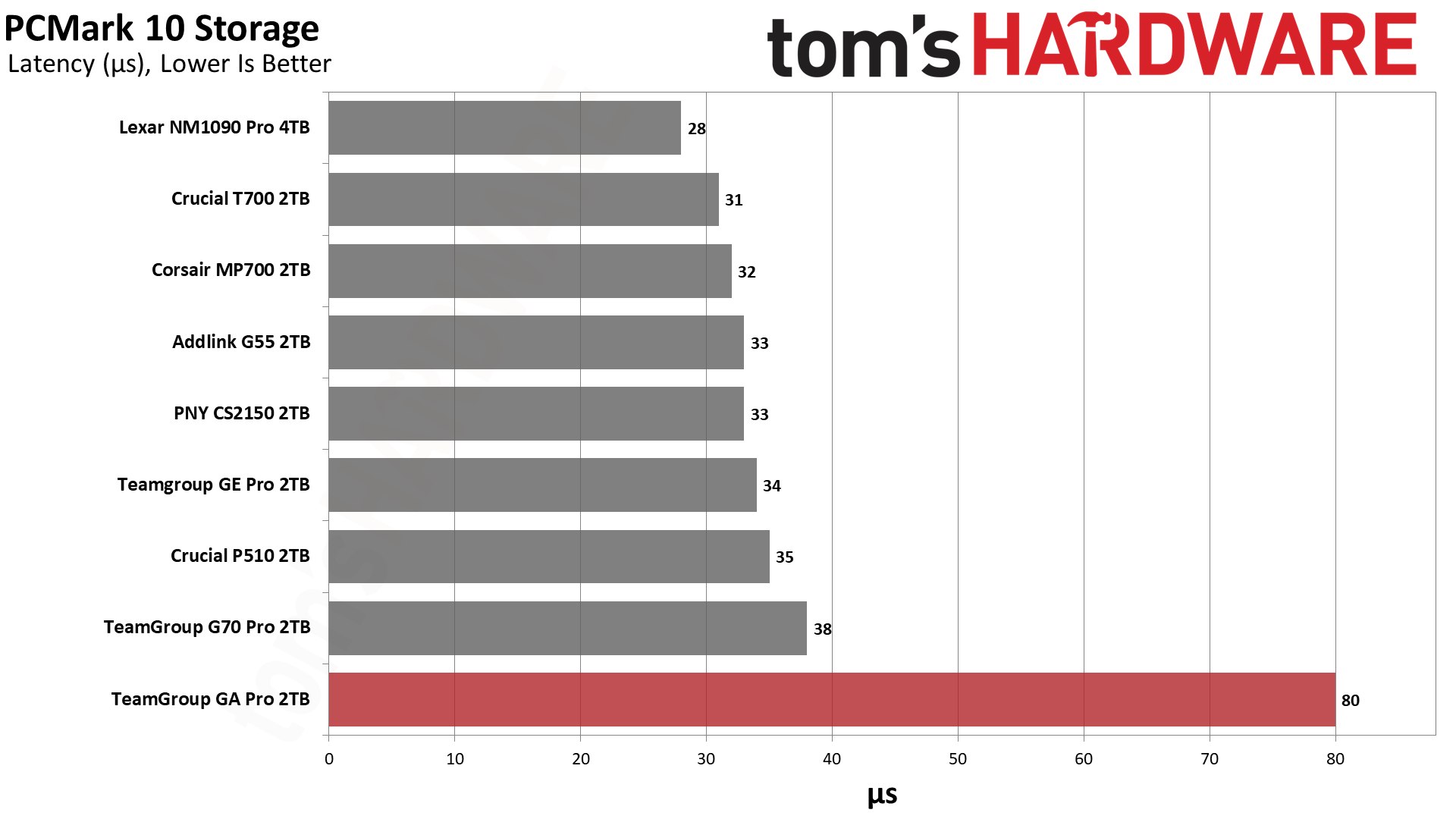
We see the same issue in PCMark. Terrible latency leads to terrible overall results. The drive may not be slow intrinsically, but it might as well be considered as such.
Our hypothesis here, since the problem is consistent, is that the drive is unintentionally throttling. Usually this happens due to heat, but saying “heat” is not fully addressing the problem. That is, it’s not necessarily the heat causing the issue but how the drive and firmware detect and handle it. We remember the days of prototype PCIe 5.0 controllers, mainly from Phison, where flash temperatures were not properly calibrated and caused unintentional throttling. It’s possible something similar is happening here, given how hot the controller runs (see our power and temperature section), but the early takeaway for now is that this is a “solved” problem that InnoGrit is struggling with on this drive for one reason or another.
Console Testing — PlayStation 5 Transfers
The PlayStation 5 is capable of taking one additional PCIe 4.0 or faster SSD for extra game storage. While any 4.0 drive will technically work, Sony recommends drives that can deliver at least 5,500 MB/s of sequential read bandwidth for optimal performance. Based on our extensive testing, PCIe 5.0 SSDs don’t bring much to the table and generally shouldn’t be used in the PS5, especially as they may require additional cooling. Check our Best PS5 SSDs article for more information.
Our testing utilizes the PS5’s internal storage test and manual read/write tests with over 192GB of data both from and to the internal storage. Throttling is prevented where possible to see how each drive operates under ideal conditions. While game load times should not deviate much from drive to drive, our results can indicate which drives may be more responsive in long-term use.
Tom's HardwareTom's HardwareTom's Hardware
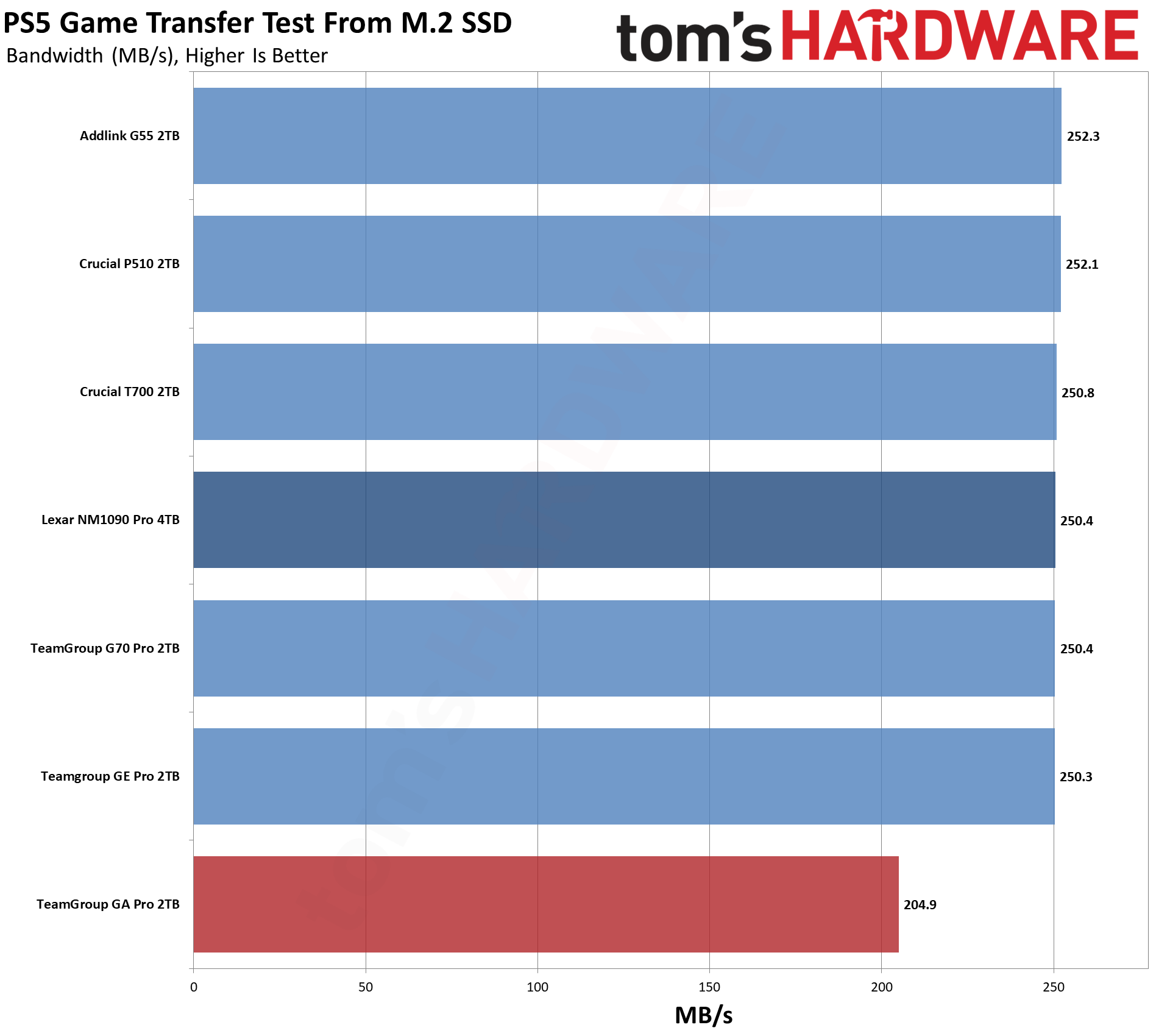
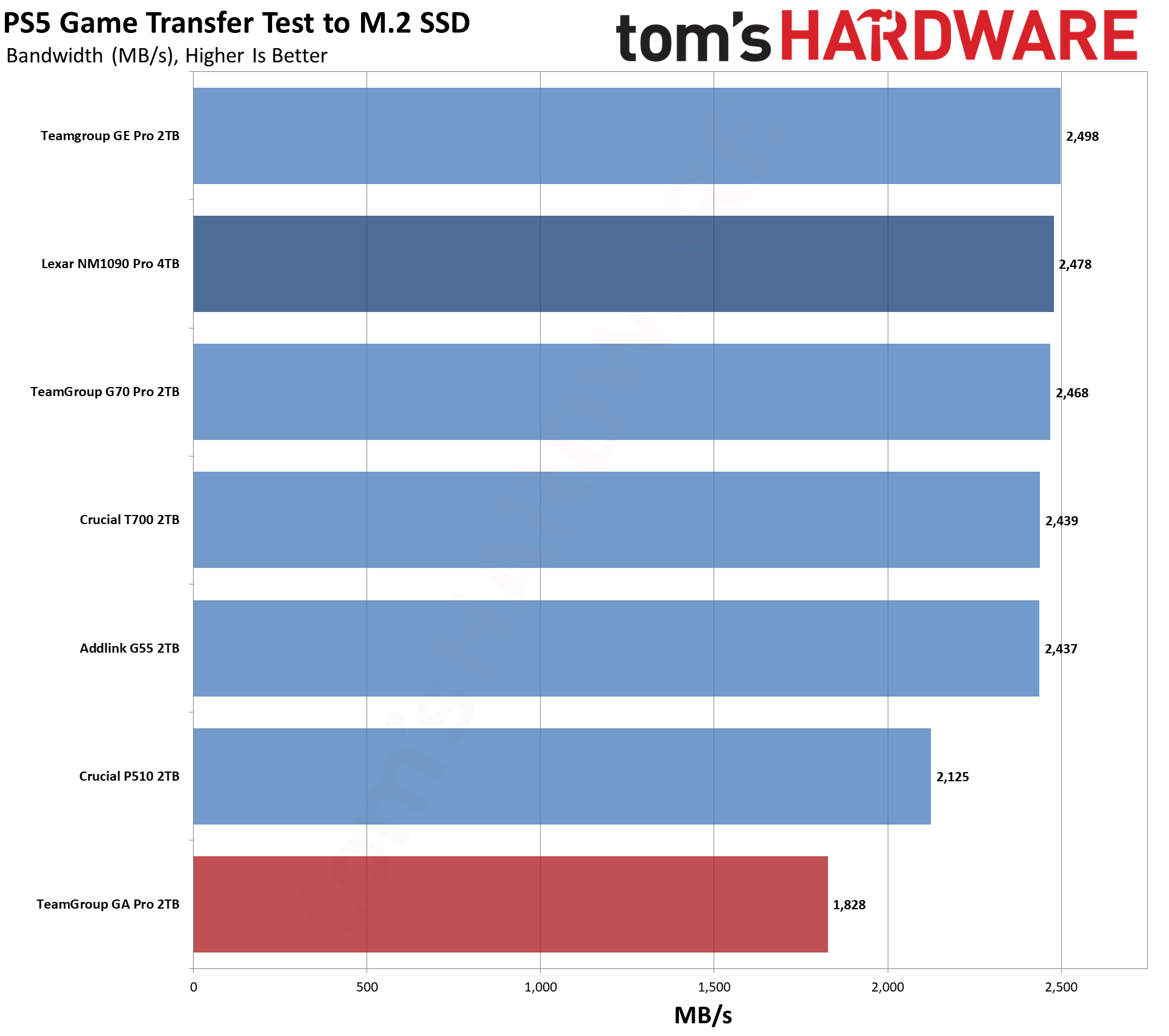
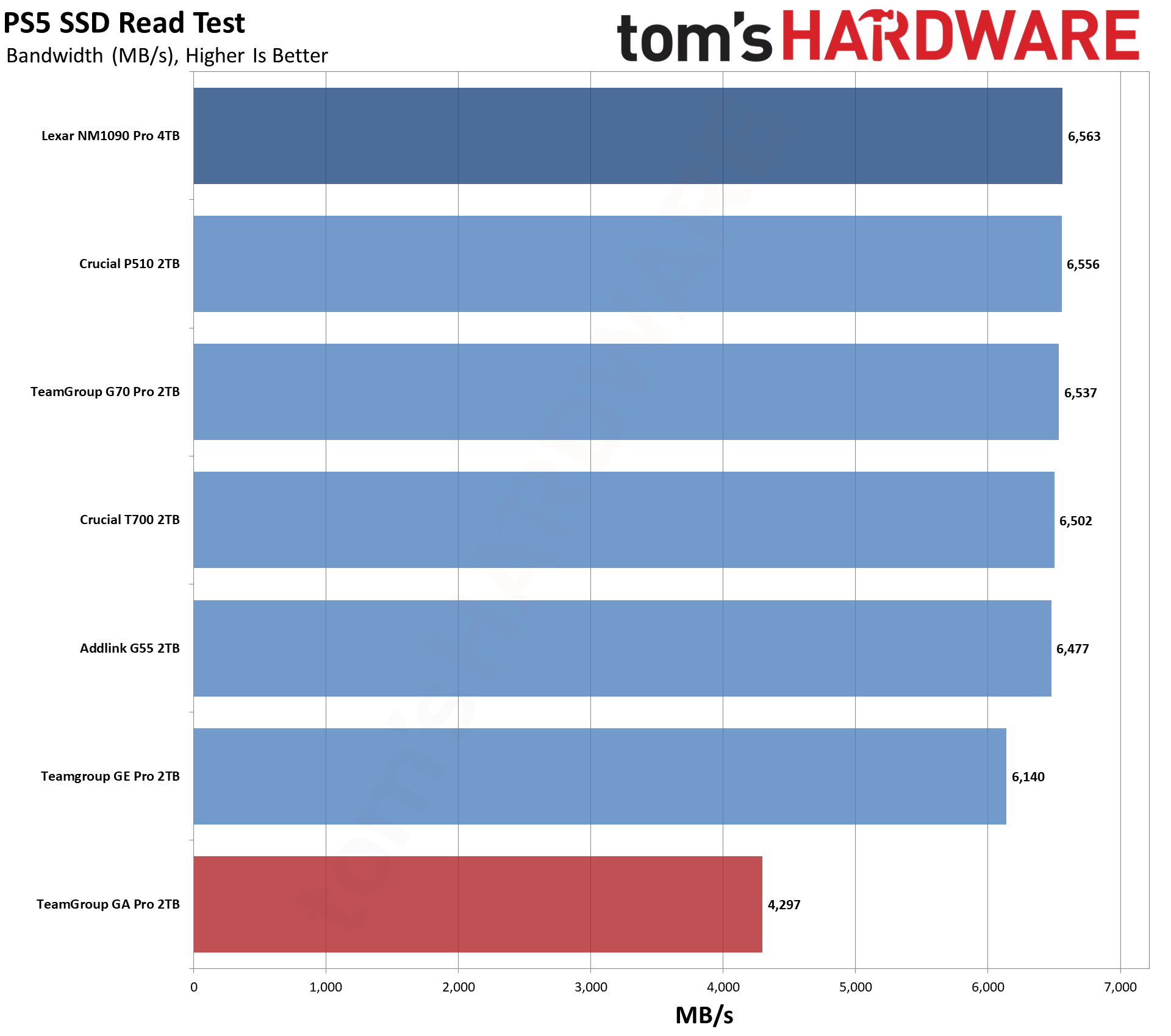
We usually don’t worry about the PS5 with PCIe 5.0 drives, as even the slowest ones are plenty for the console, but we wanted to be sure with this one. The drive works but does not perform that well. Given how brief this testing can be, and because it’s limited to PCIe 4.0 speeds, we don’t believe the drive is throttling. It’s more likely the same latency issue we saw in the trace tests, or a larger firmware issue.
Transfer Rates — DiskBench
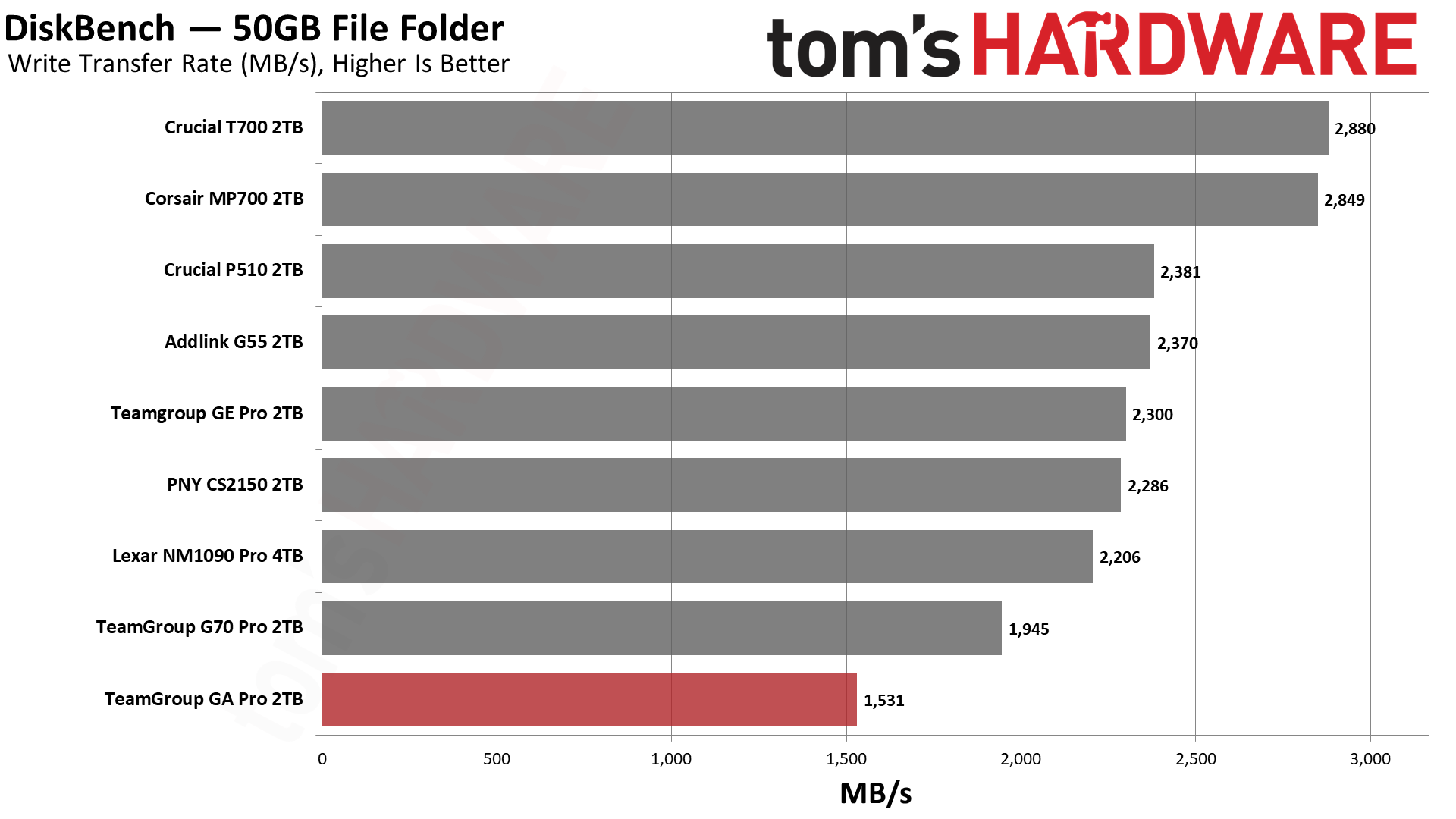
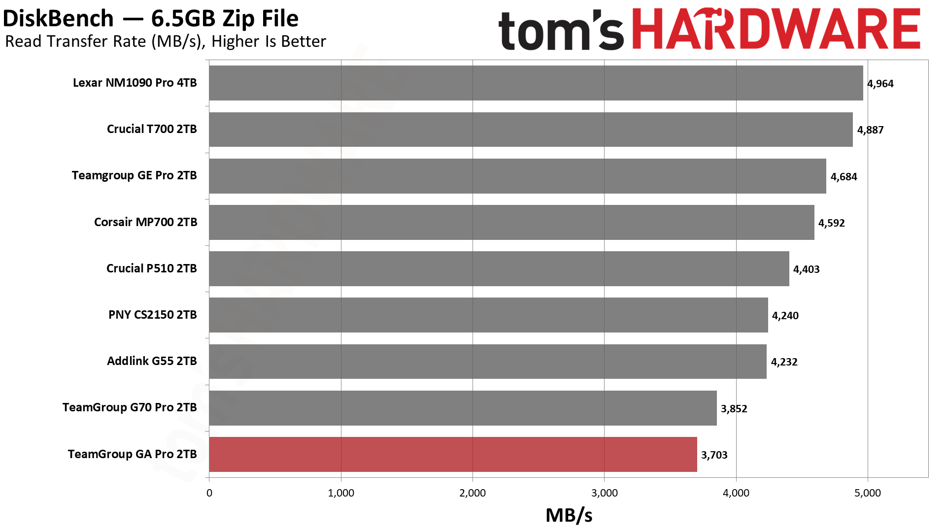
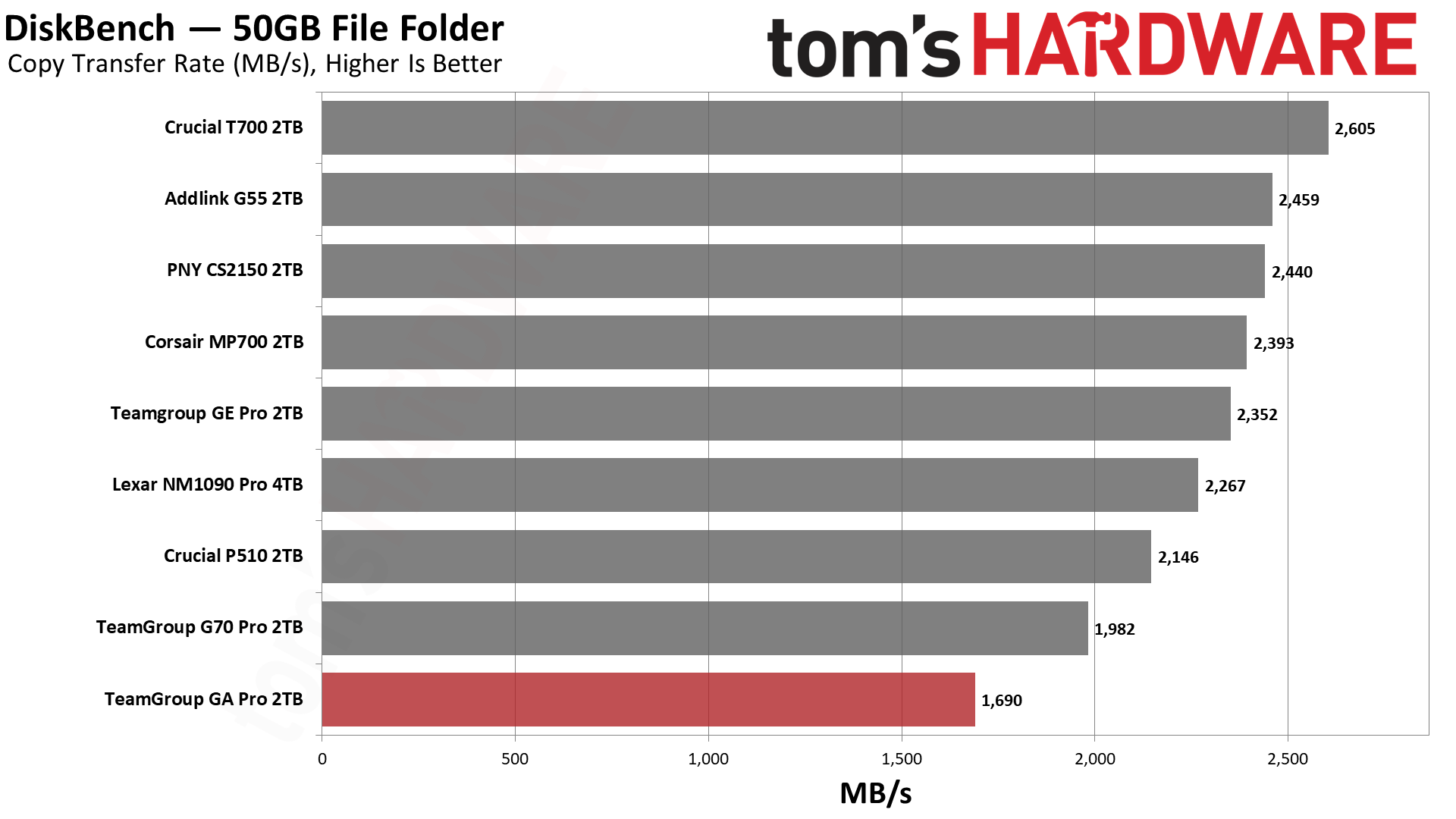
We use the DiskBench storage benchmarking tool to test file transfer performance with a custom 50GB dataset. We write 31,227 files of various types, such as pictures, PDFs, and videos to the test drive, then make a copy of that data to a new folder, and follow up with a reading test of a newly written 6.5GB zip file. This is a real-world type workload that fits into the cache of most drives.
Tom's HardwareTom's HardwareTom's Hardware
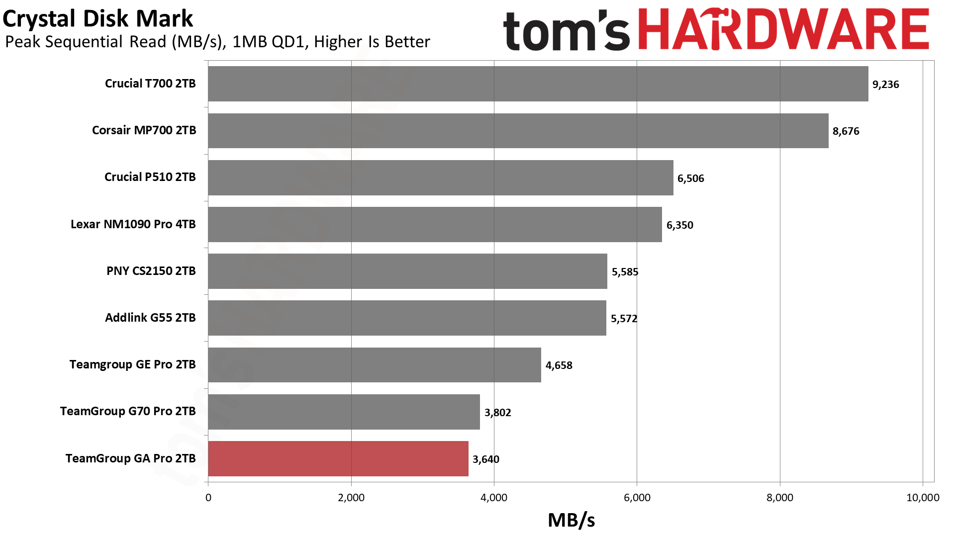
The GA Pro also ends up dead last in DiskBench, which also requires explanation. The drive has a very small cache for its size and generation, something that is also OEM- or NAS-like rather than what we’d expect from a normal retail drive, but it’s large enough to fit this test. Either the cache was not fully emptied in testing, which generally would also be linked to firmware, or we’re having more issues here from the previously mentioned flaw. The drive is also slower with reads because the reads in this test are at a queue depth of 1, where the drive is known to have issues; this was affirmed by TeamGroup when we asked.
Synthetic Testing — ATTO / CrystalDiskMark
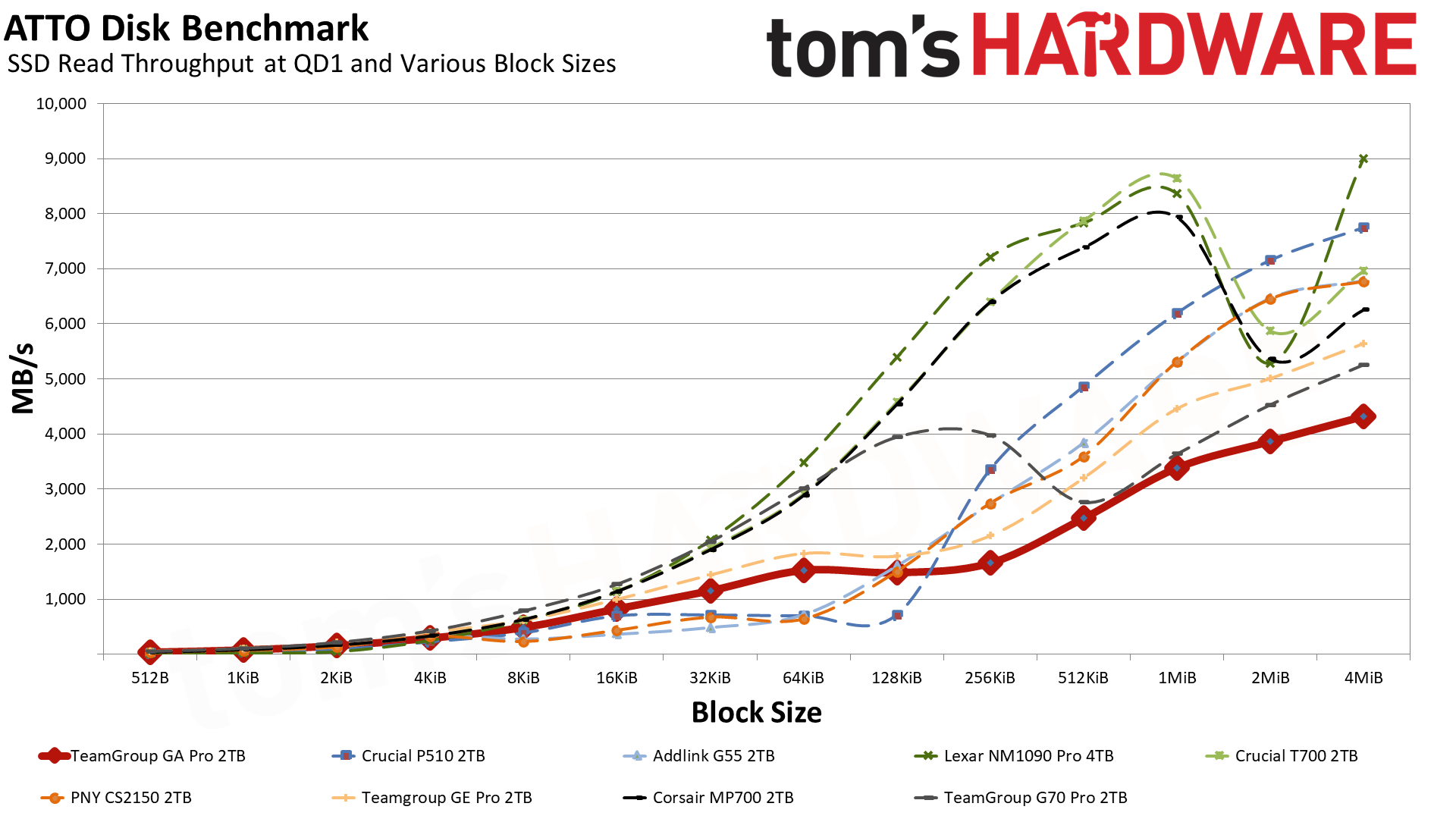
ATTO and CrystalDiskMark (CDM) are free and easy-to-use storage benchmarking tools that SSD vendors commonly use to assign performance specifications to their products. Both of these tools give us insight into how each device handles different file sizes and at different queue depths for both sequential and random workloads.
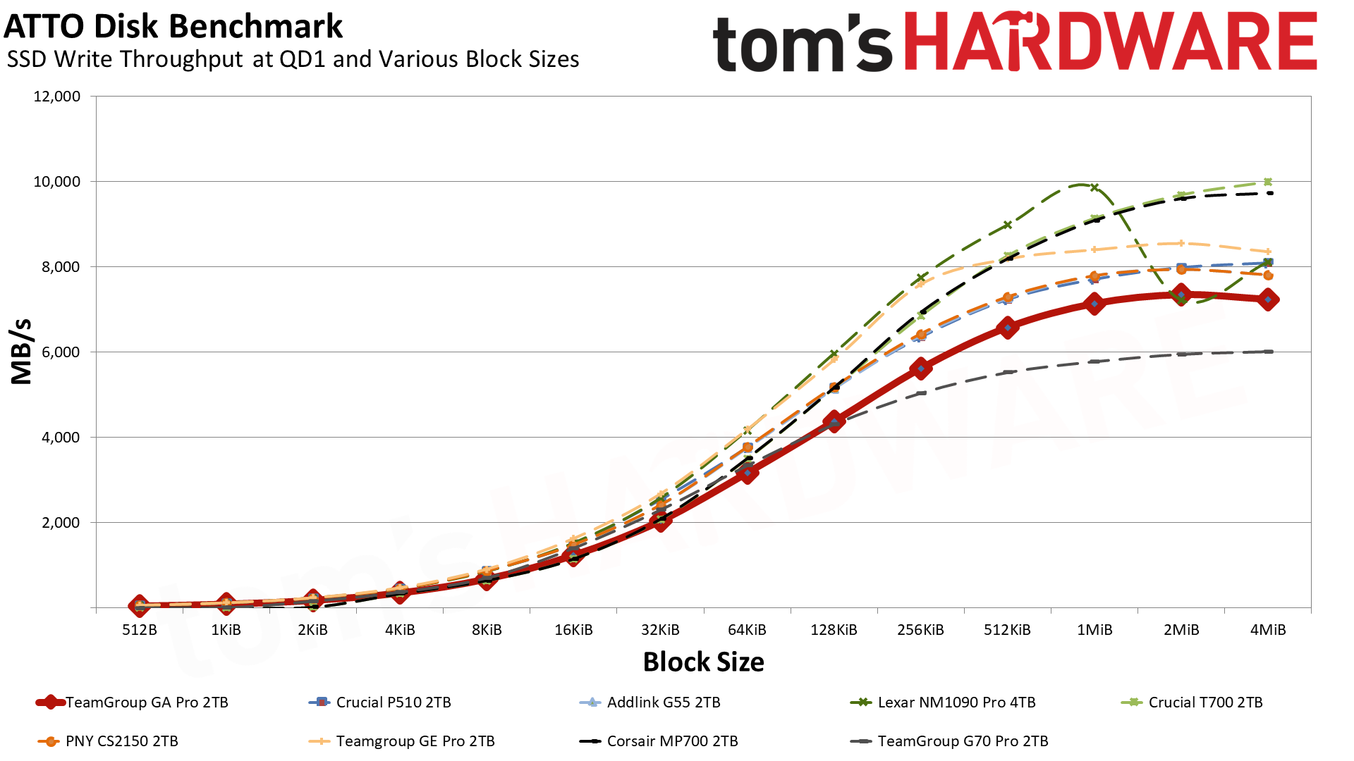
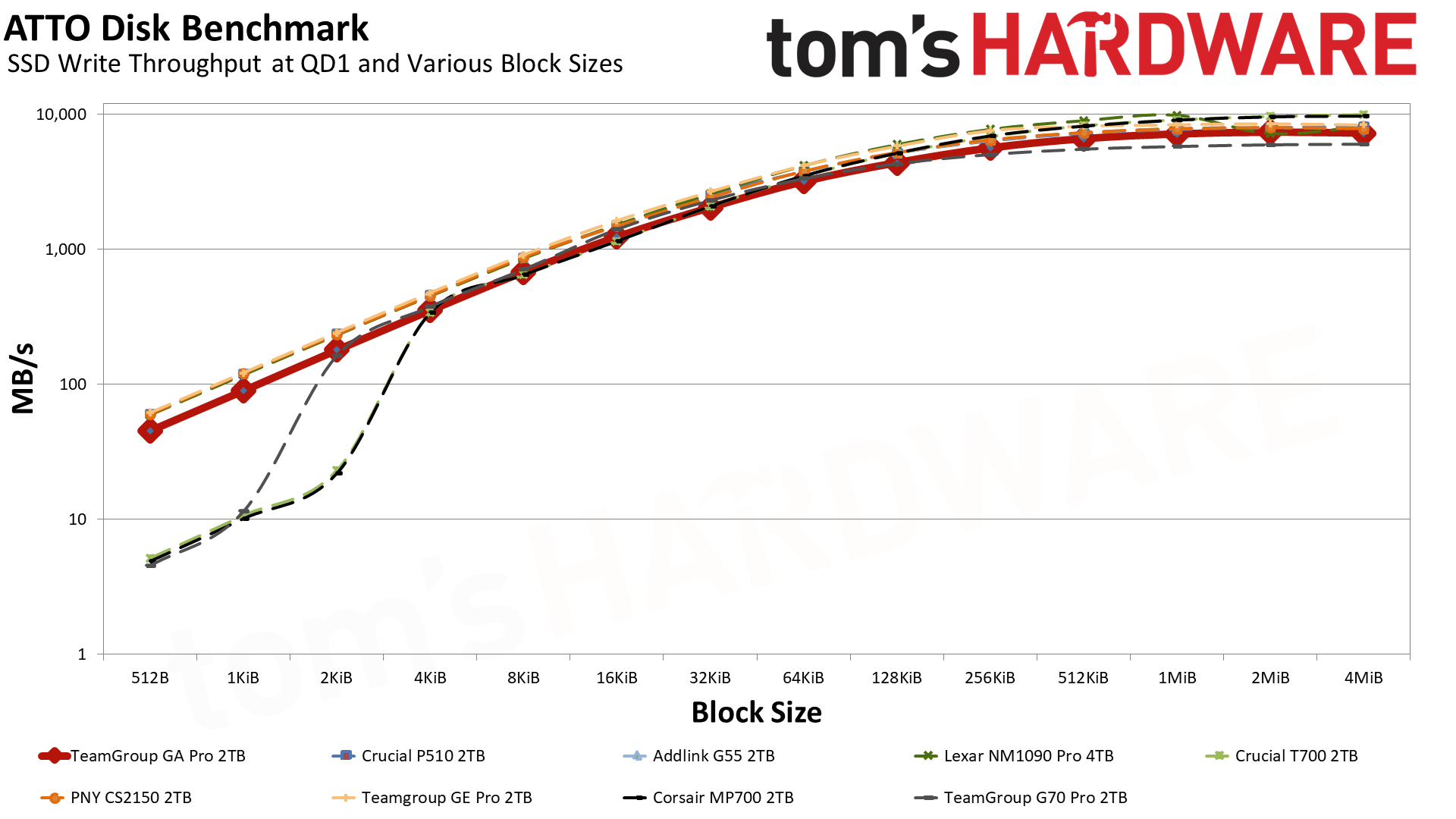
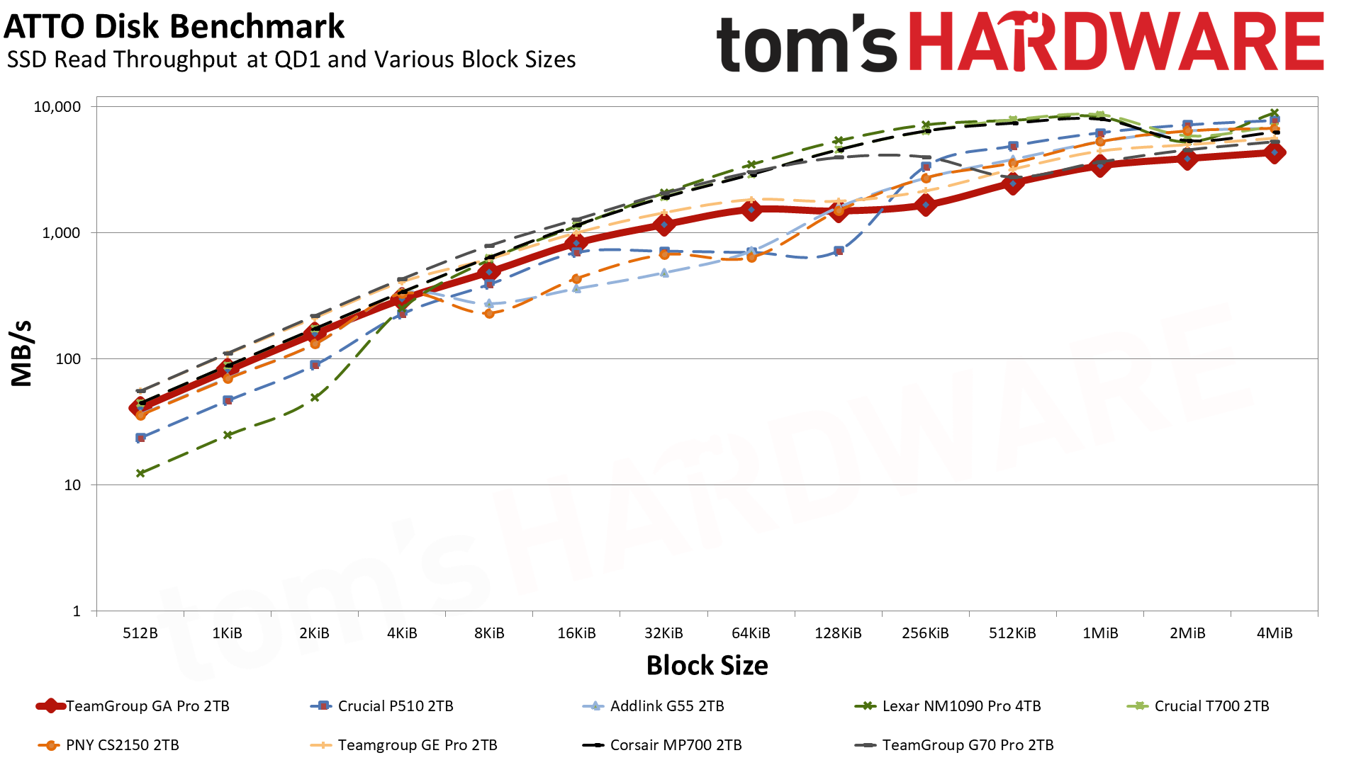
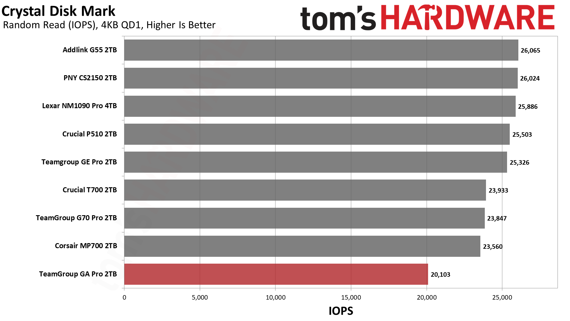
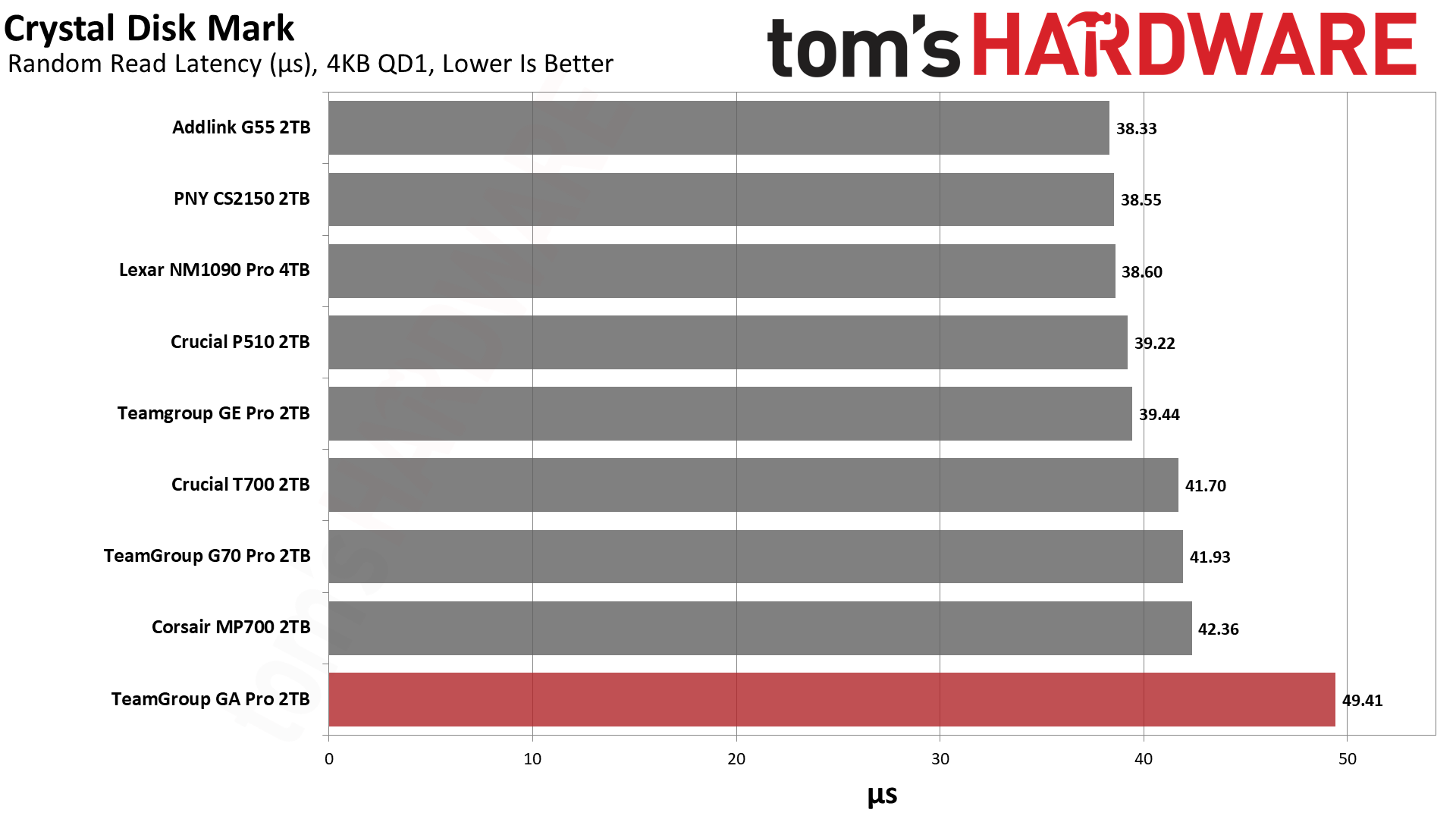
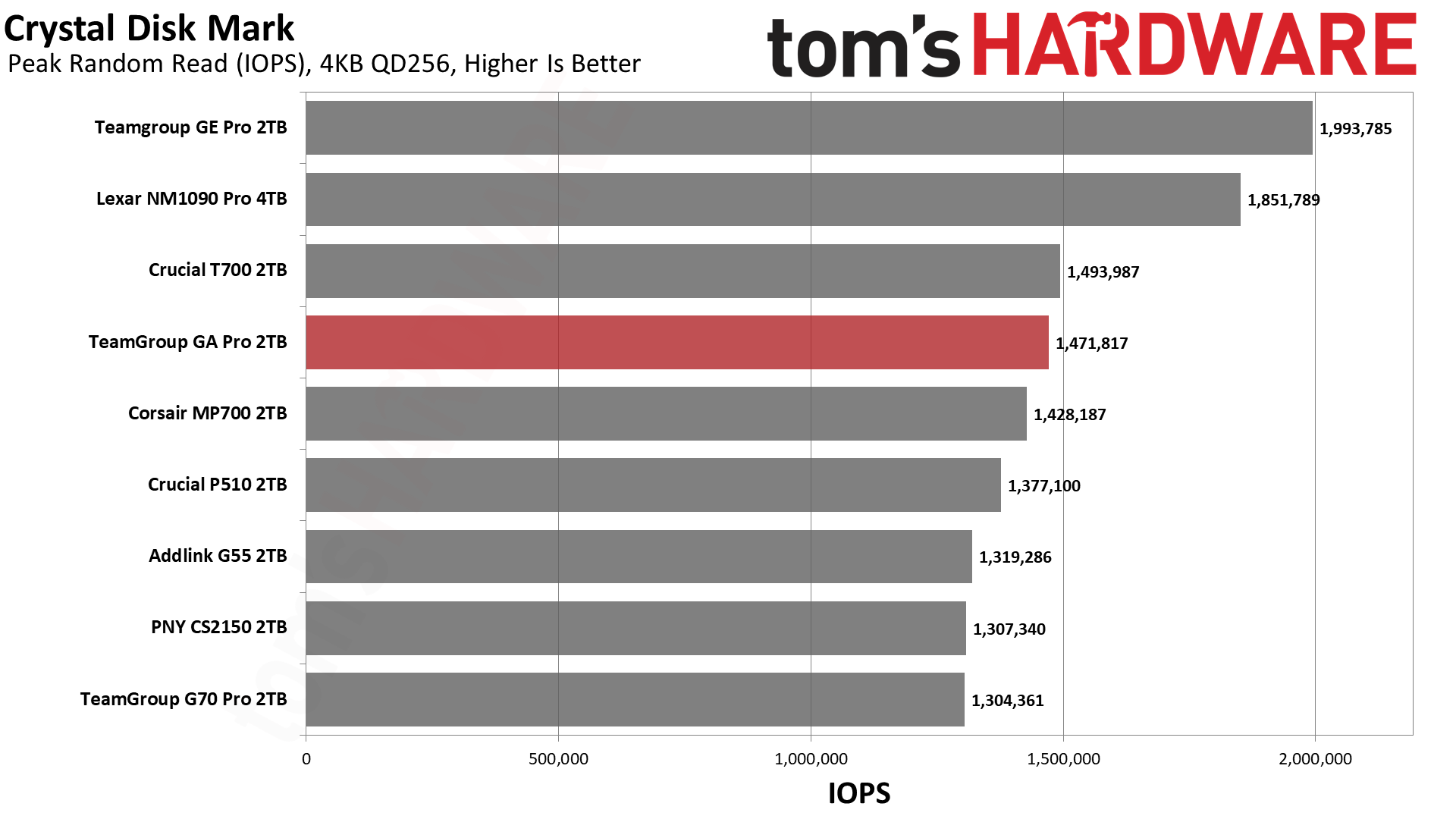
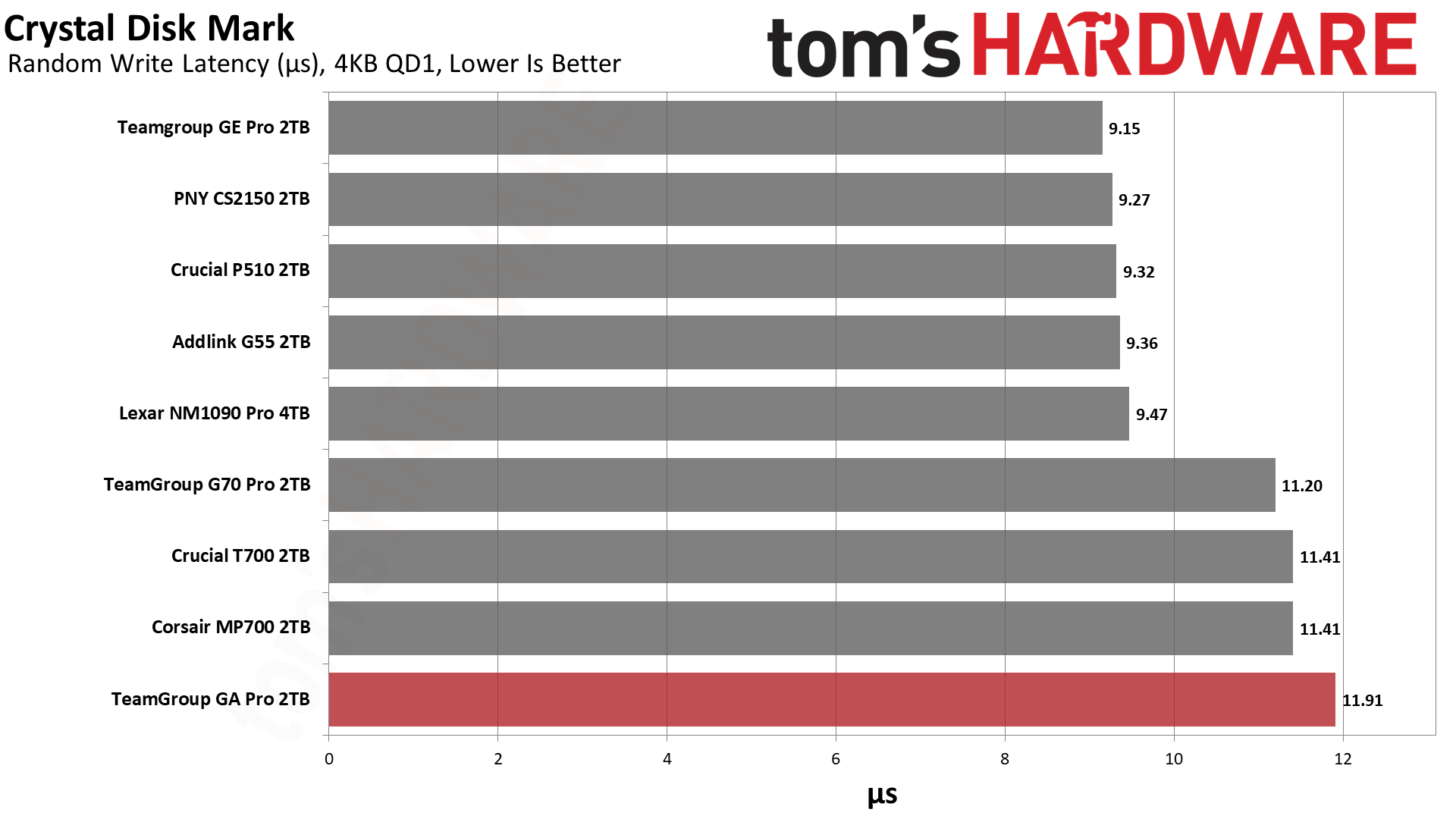
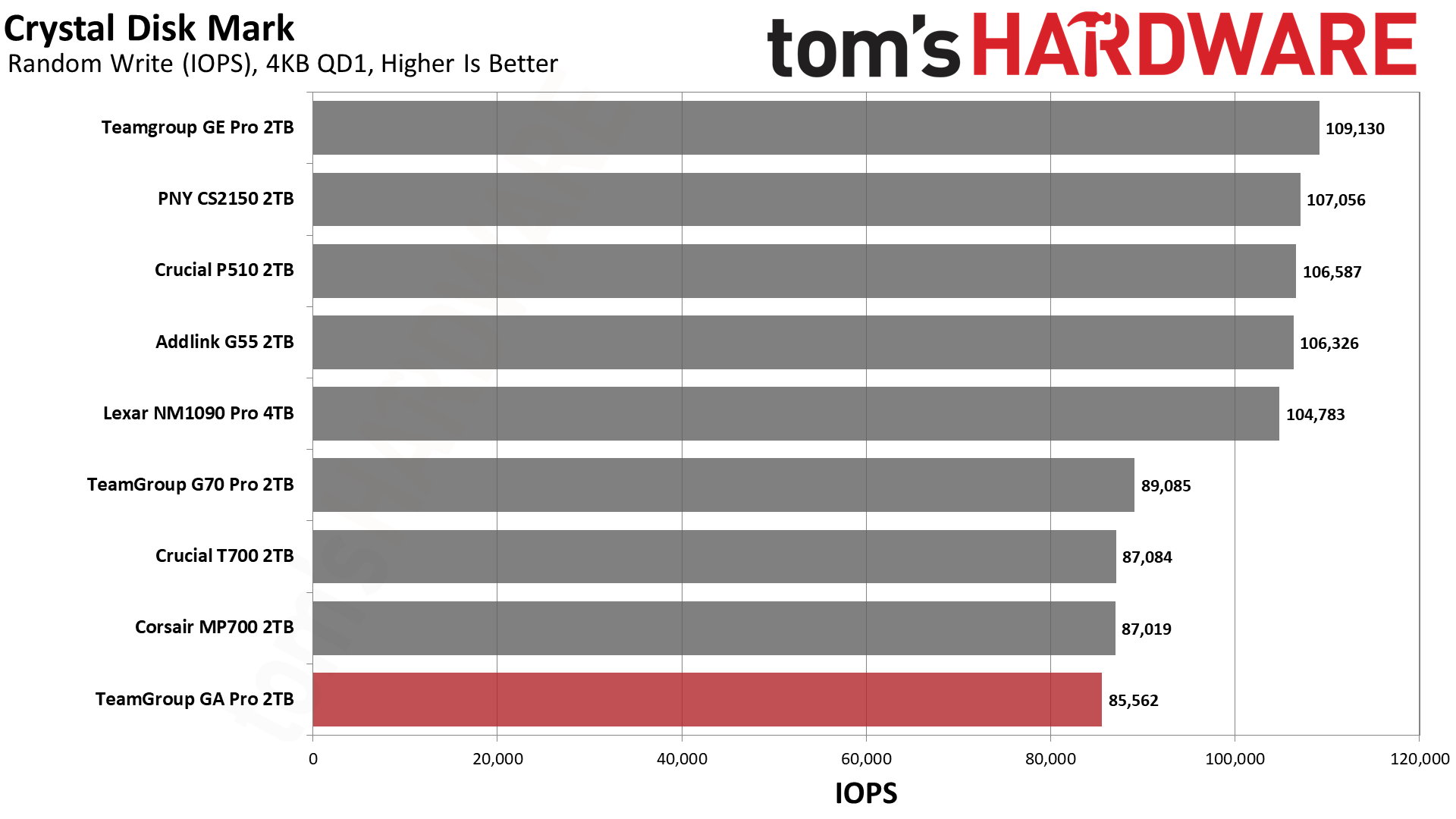
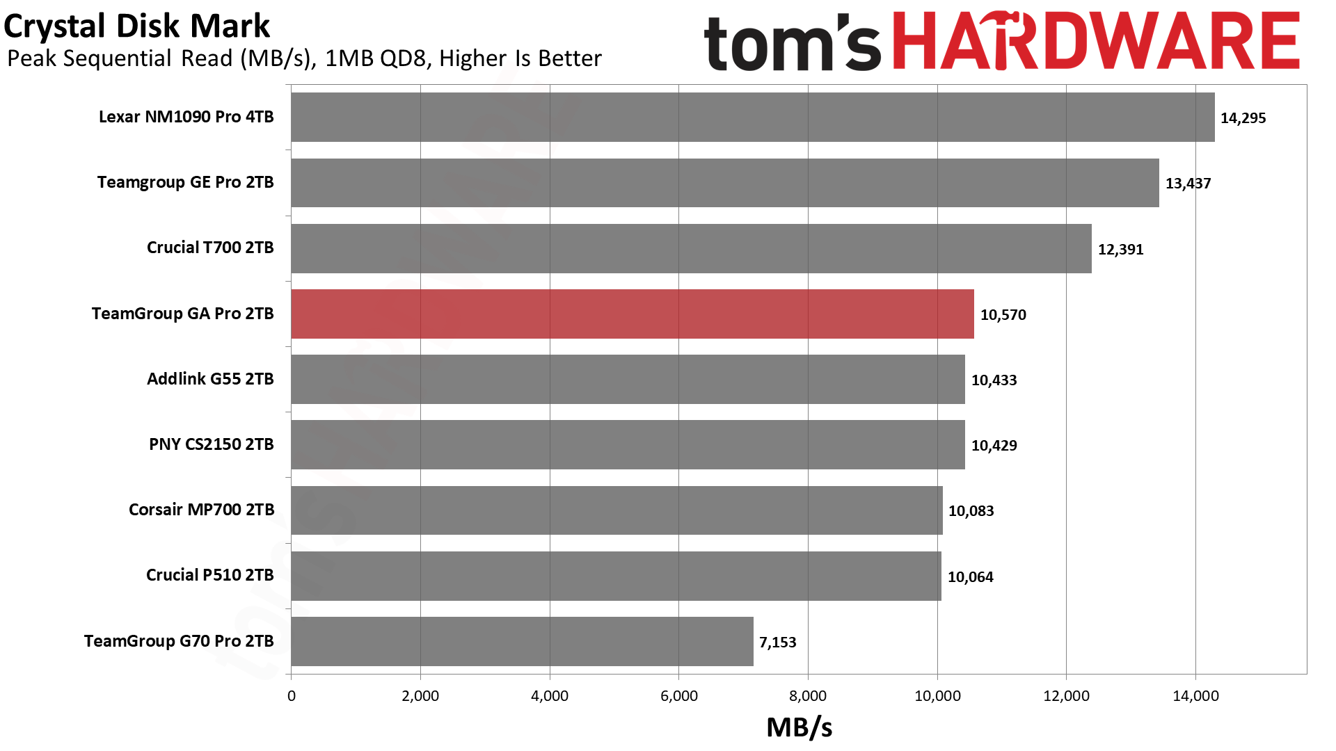
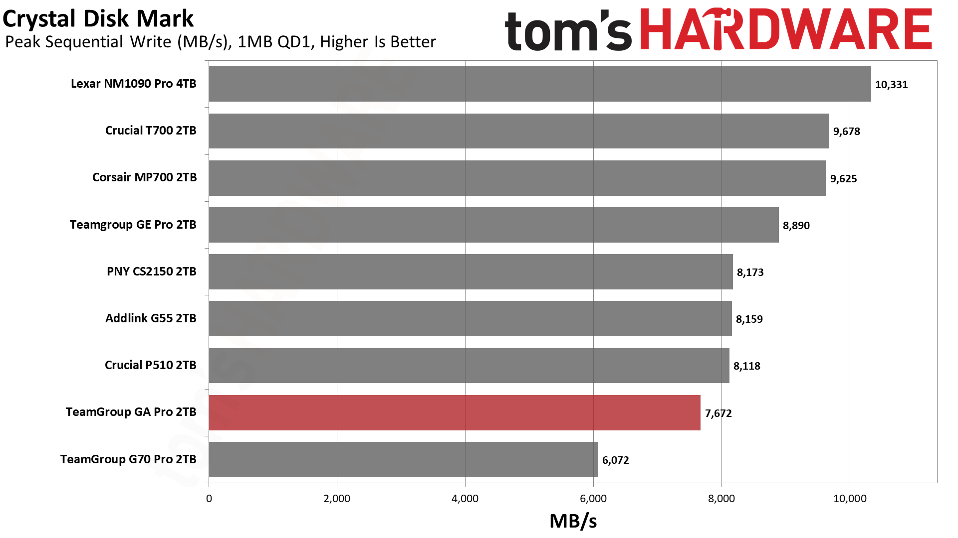
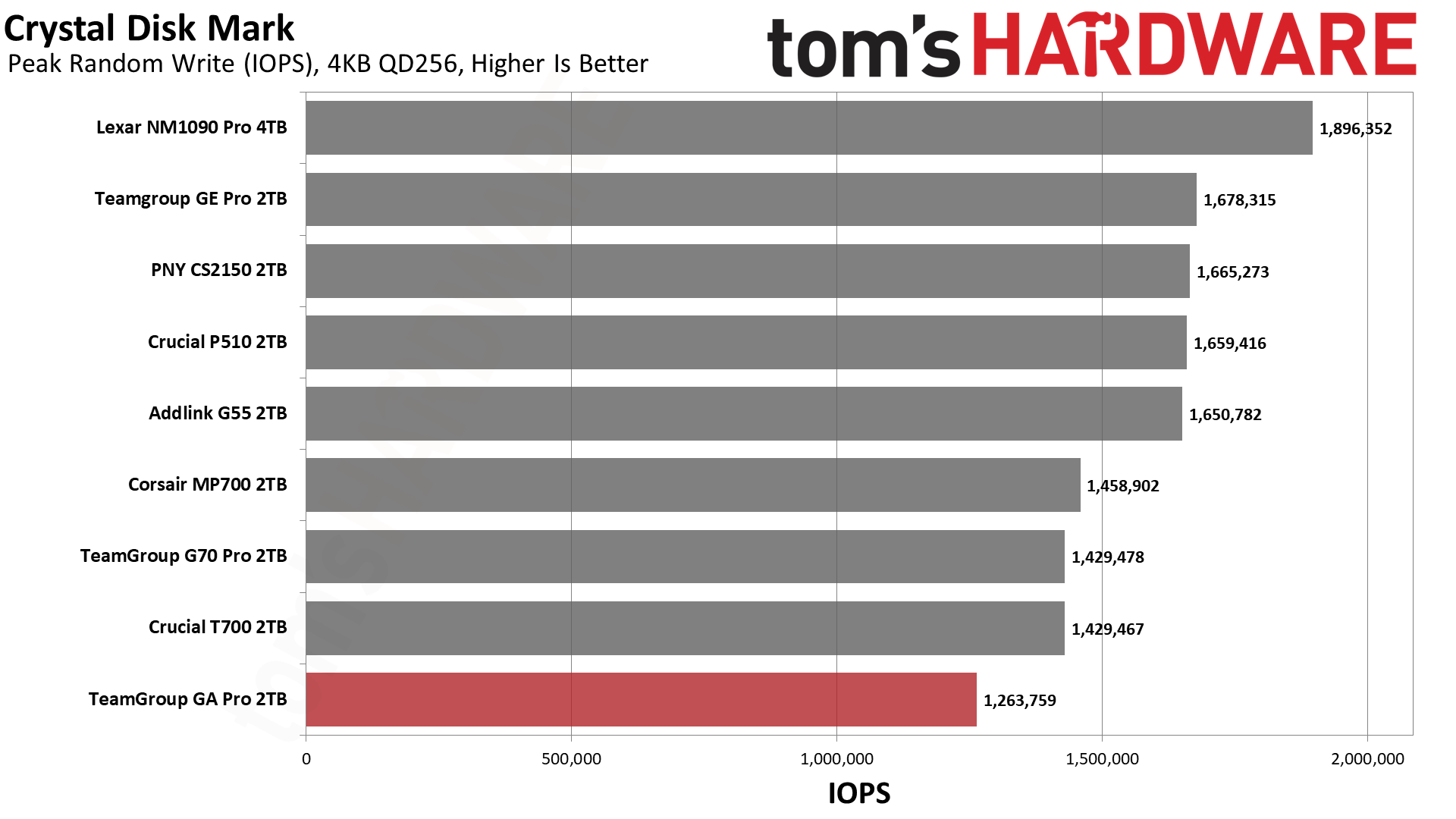
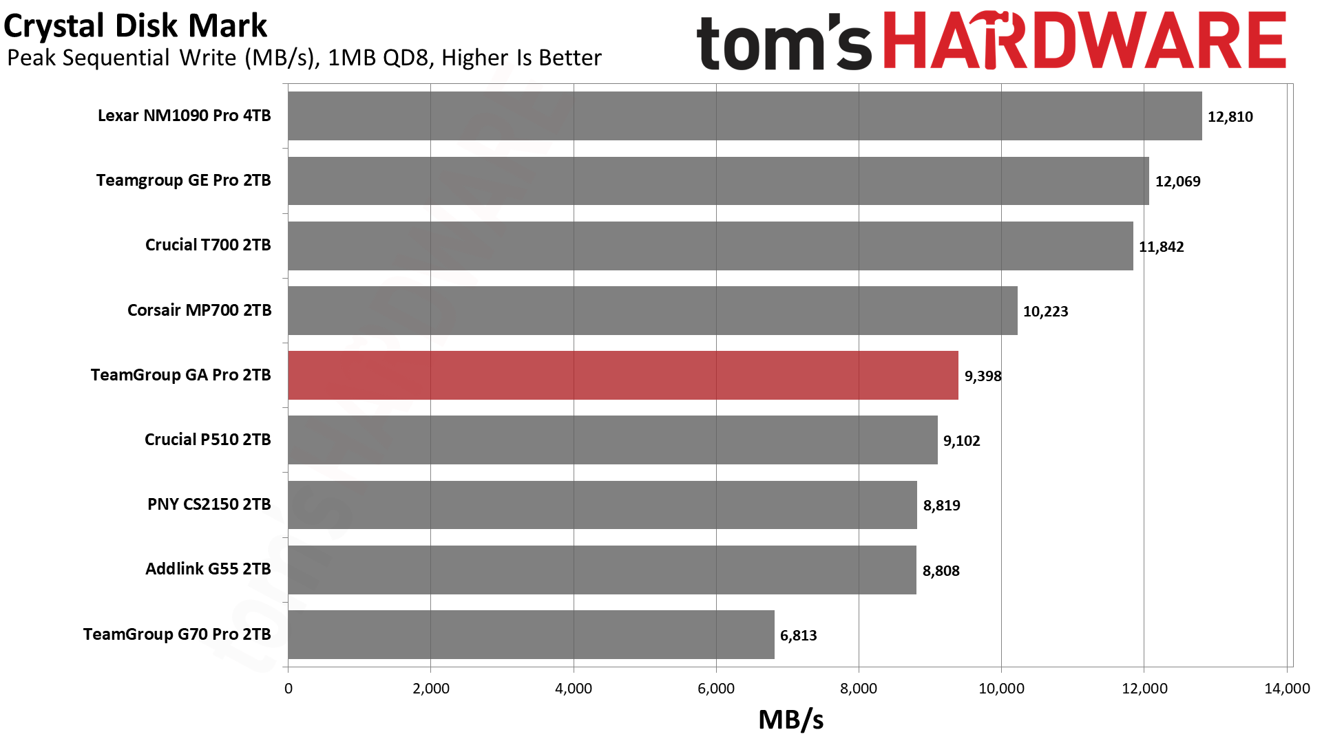
The GA Pro isn’t actually all bad here, with reasonable ATTO curves and even some okay marks in CDM. 4KB latency is still higher than expected, and that hurts this drive for everyday use. On the other hand, it can mete out some decent sequential performance, especially at QD8. TeamGroup told us that this is what the drive was designed for, so that lines up. Keep in mind, this drive isn’t going to keep up with PCIe 5.0 drives rated for higher speeds. Instead, to keep it on the positive side, at QD8 it does very well against drives with similar specs.
Sustained Write Performance and Cache Recovery
Official write specifications are only part of the performance picture. Most SSDs implement a write cache, which is a fast area of pseudo-SLC (single-bit) programmed flash that absorbs incoming data. Sustained write speeds can suffer tremendously once the workload spills outside of the cache and into the "native" TLC (three-bit) or QLC (four-bit) flash. Performance can suffer even more if the drive is forced to fold, the process of migrating data out of the cache in order to free up space for further incoming data.
We use Iometer to hammer the SSD with sequential writes for 15 minutes to measure both the size of the write cache and performance after the cache is saturated. We also monitor cache recovery via multiple idle rounds. This process shows the performance of the drive in various states including the steady state write performance.
Tom's HardwareTom's HardwareTom's Hardware
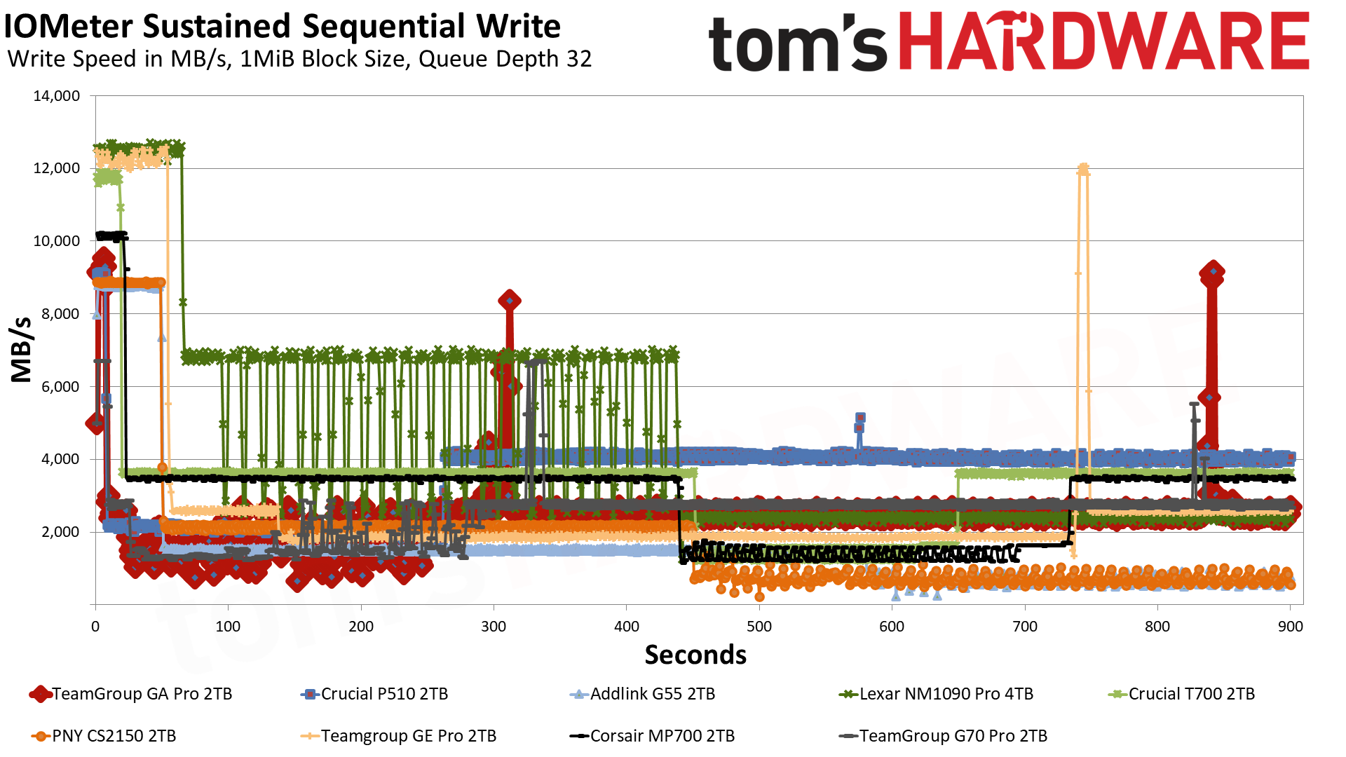
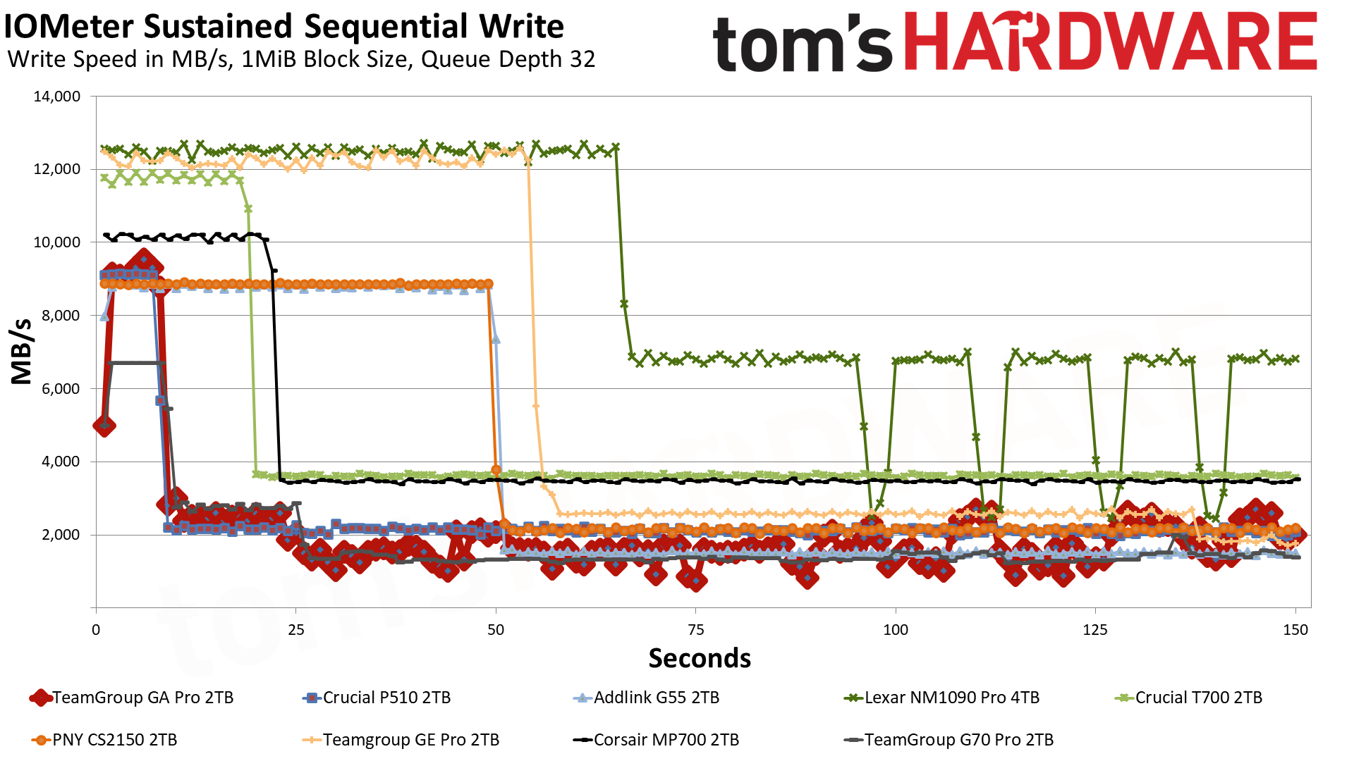
The GA Pro’s fastest mode, pSLC, or what’s called the cache, writes at around 9.2 GB/s. This is respectable for the drive’s speed class and beats any PCIe 4.0 drive, but also doesn’t set records. It only writes at this speed for approximately 7 seconds, which is incredibly short, and means the cache is only about 69 GB in size. This is small in general, small for a 2TB drive, and very small for a modern, PCIe 5.0 drive. It’s not unheard of, as we’ve seen caches around this size on some drives to improve “quality of service,” which basically means keeping the drive performing consistently even when the cache runs out.
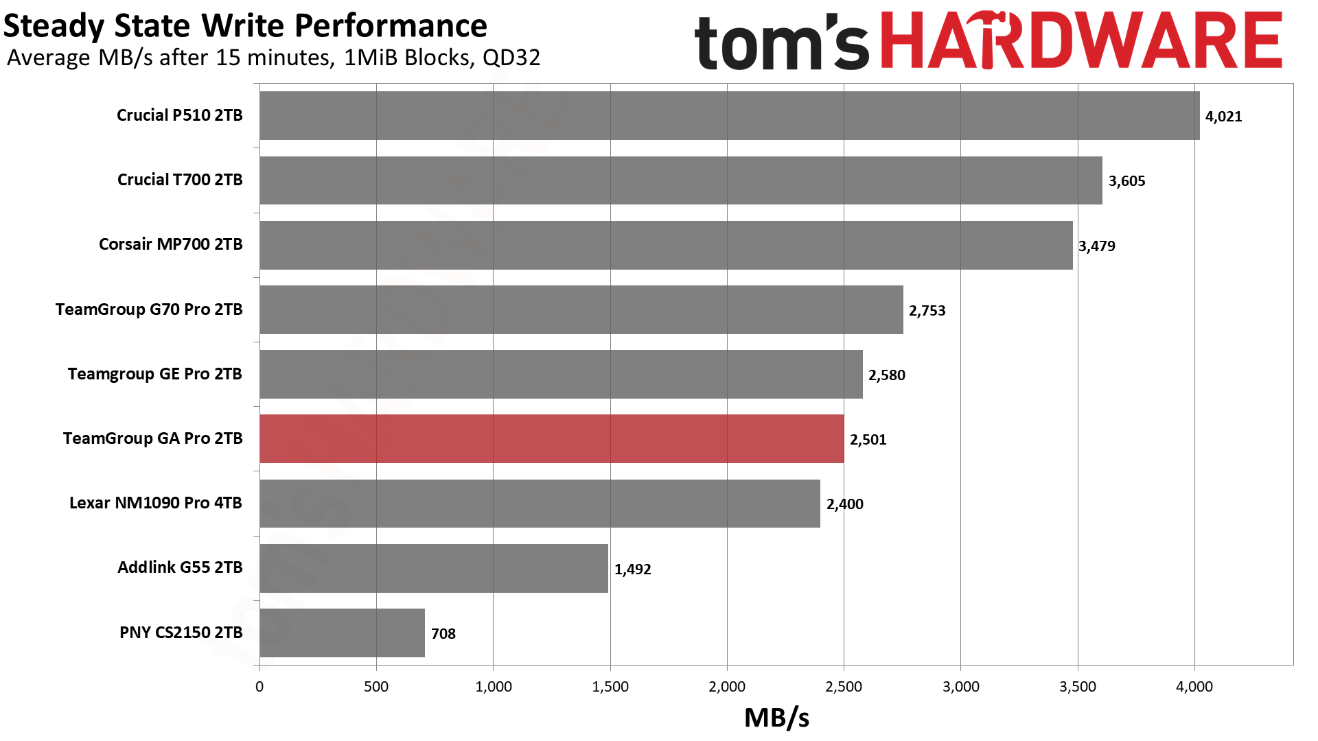
We don’t see that, per se, after the cache runs out here. The drive initially acts in an erratic manner, although eventually it does hit a steady speed around 2.5 GB/s. This isn’t too bad, but the drive should be able to muster a little bit more: the G70 Pro, with the same YMTC flash and an even smaller cache, manages about 2.75 GB/s. Still, it’s fast enough to be useful for some applications. TeamGroup suggested this is one area the drive was designed to be good at, and while we can’t agree with that 100%, we do think its current arrangement is, on paper, good for something like write caching. It would be better if things were smoothed out, maybe through firmware, and we would absolutely recommend a good heatsink for that type of workload on this drive.
Power Consumption and Temperature
We use the Quarch HD Programmable Power Module to gain a deeper understanding of power characteristics. Idle power consumption is an important aspect to consider, especially if you're looking for a laptop upgrade, as even the best ultrabooks can have mediocre stock storage in terms of capacity and performance. Desktops are often more performance-oriented with less support for power-saving features, so we show the worst-case for idle.
Some SSDs can consume watts of power at idle while better-suited ones sip just milliwatts. Average workload power consumption and max consumption are two other aspects of power consumption, but performance-per-watt, or efficiency, is more important. A drive might consume more power during any given workload, but accomplishing a task faster allows the drive to drop into an idle state more quickly, ultimately saving energy.
For temperature recording, we currently poll the drive’s primary composite sensor during testing with a ~22°C ambient. Our testing is rigorous enough to heat the drive to a realistic ceiling temperature, but real-world temperatures will vary due to the environment and workload factors.
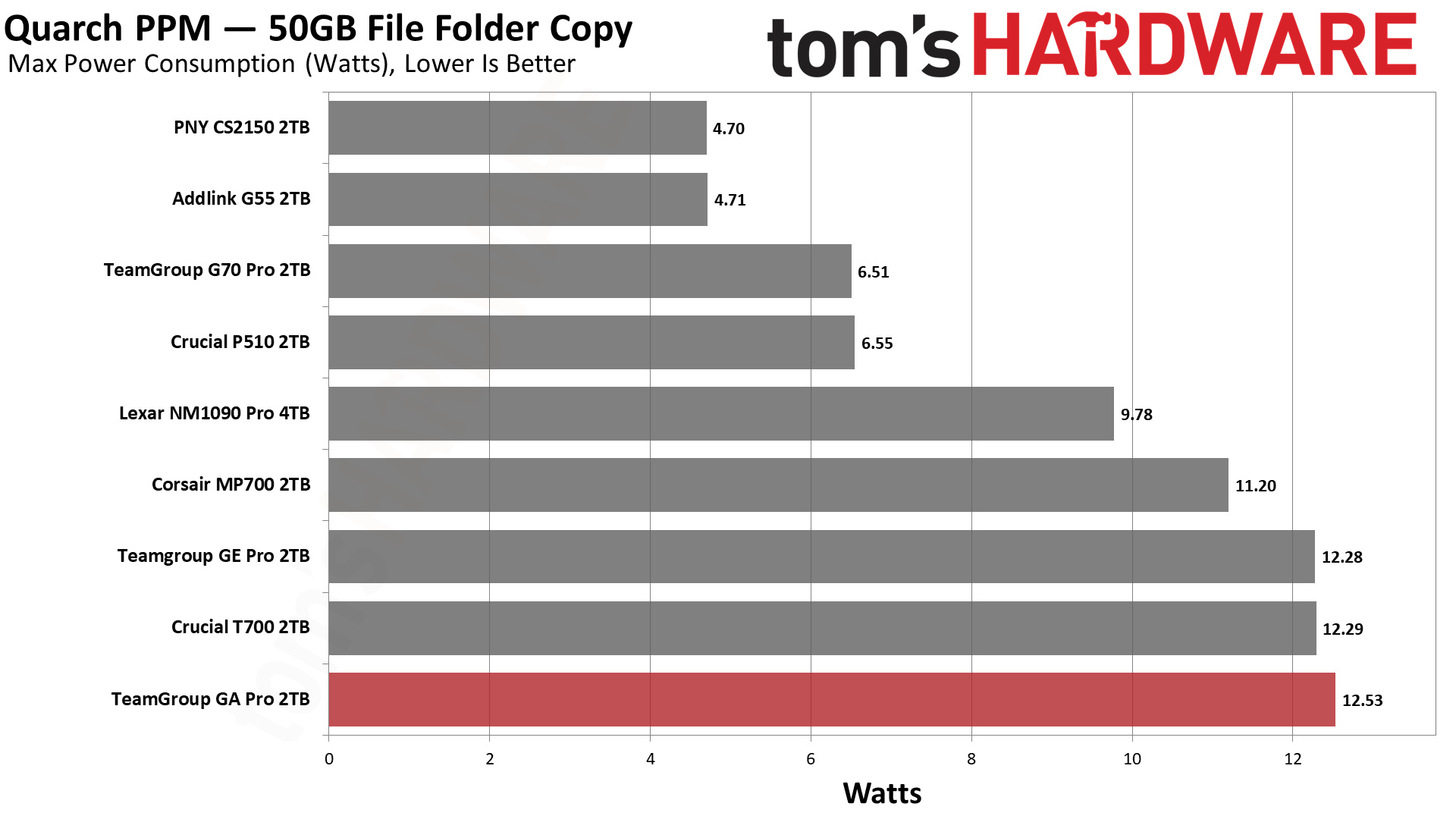
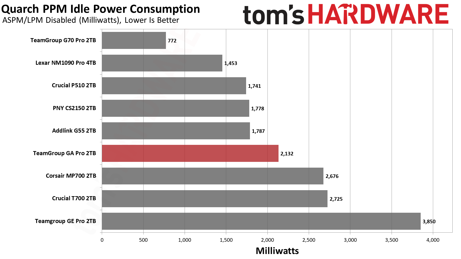
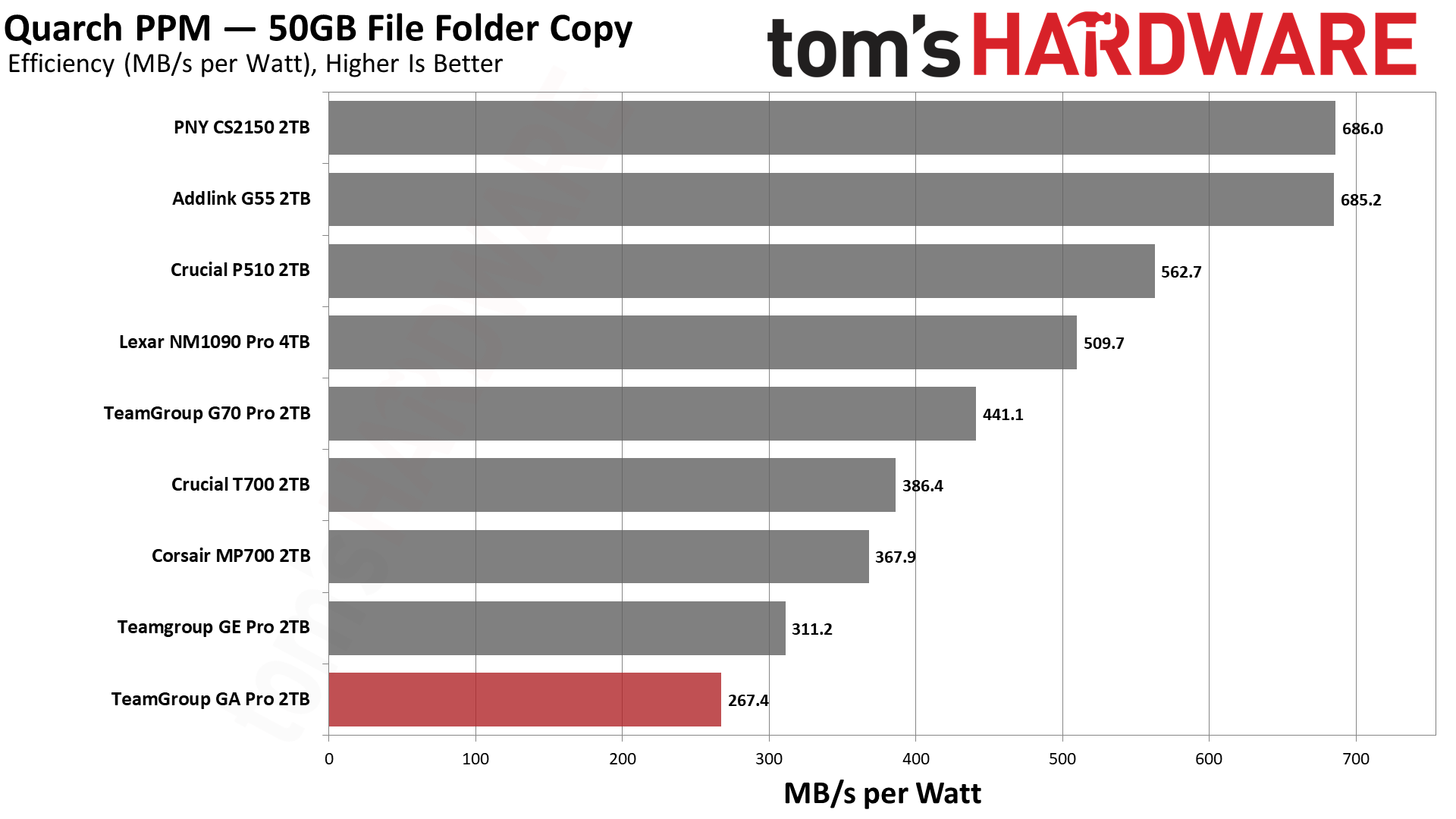
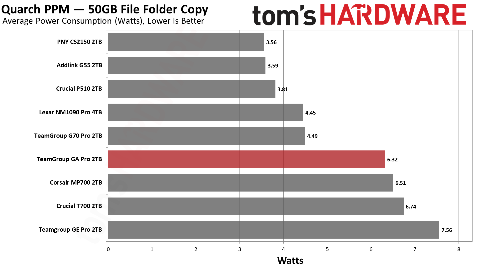
At this point in the review, you’re probably thinking to yourself: I bet the GA Pro isn’t very power-efficient, either. You’d be correct; it finishes last in our lineup. That comes down to its slow DiskBench copy speed, which our efficiency metric is based on, paired with high power draw: the GA Pro averages 6.32W, fourth-highest in our lineup, and peaks at 12.53W, the highest. Also, its hardware is already known to be inefficient even compared to comparables like a Phison E26 and Micron TLC on the MP700; see the GE Pro. We also don’t really expect great power efficiency out of a drive like this. That said, yeah, don’t get this drive if you care about that. One thing we’ll add is that TeamGroup’s claim about latency fits the results here: the GA Pro’s idle power consumption is significantly better than the GE Pro’s.
Temperature-wise, well, what can we say? The three sensors reported maximum temperatures of 61, 72, and 92 degrees Celsius. The 92-degree reading is most likely the controller, which held at 88 degrees or higher for over 90% of our sustained write test. The drive’s 90-degree warning threshold applies to the composite sensor, which peaked at 72 degrees, and it stayed below that threshold. But the controller holding steady at around 89 degrees in some cases suggests the firmware may be working around that temperature instead. Either way, yes, this drive runs hot. Mind, this is with cooling, so you would definitely want to be prepared to handle this one.
We use an Alder Lake platform with most background applications such as indexing, Windows updates, and antivirus disabled in the OS to reduce run-to-run variability. Each SSD is prefilled to 50% capacity and tested as a secondary device. Unless noted, we use active cooling for all SSDs.
TeamGroup GA Pro Bottom Line
We test many, many drives and only rarely, exceptionally, do we consider giving out a perfect score. That’s because the perfect drive is essentially a unicorn. The same goes the other way, too: to get our very worst rating, a drive would have to be truly awful. Now, the TeamGroup GA Pro is among the worst drives I’ve handled in my tenure, but I’ve heard of many worse. Drives that fail at the drop of a hat, ones plagued with firmware issues, ones with low-grade flash, ones with PCIe 3.0 or worse performance. They exist, and the GA Pro is not one of these. We also reviewed tons of drives from TeamGroup; this is a known brand that also communicated to us the need for a firmware revision, which makes us feel like the InnoGrit controller choice is the biggest issue here.
(Image credit: Tom's Hardware)
The GA Pro is an odd drive, anyway, because it’s not fast for a PCIe 5.0 drive. It’s at first-gen speeds for the high-end drives in this class, with the next two steps being 12 and 14 GB/s or so, and it ends up competing with later-arriving 10 GB/s drives that are DRAM-less and far more efficient. If you’re looking at a chart of drive generations like it was showing an evolution, this drive is halfway to being a dinosaur at this point. If we look at the problems Phison had early with the E26, we can see some misstep overlaps here. Our feeling is that TeamGroup had a rough idea of what they wanted this drive to be, and there are many hints at that, like the small cache size, and the vision never panned out. Not surprising given the controller has never done well and the consumer SSD industry at this point is exceptionally bad.
No excuses here, though. Performance is very bad for this class in many areas, especially with low QD reads, presumably due to a latency issue, which hits the drive hard. Power efficiency is also pretty bad, not unexpected, though, and the drive runs hot. That’s also expected from this hardware.
On the other hand, sustained write performance is not terrible once it steadies out, and in some high-QD situations the drive even outperforms its spec. We think TeamGroup could have slotted this into a NAS-like category or even HEDT like other early PCIe 5.0 SSDs. The cache speaks to that, although we’ve seen some Phison-based drives use a smaller cache to smooth out write performance. Which means that TeamGroup may have been targeting a similar milieu, but of course putting the GA Pro up against an E31T drive, like the P510, makes little sense to us.
We cannot recommend the drive in its current form; it needs a firmware update. With that update, and if pricing is respectable, the drive has some niche applications. It could tank some higher QD sequential workloads and let you induce less wear on your better or more important drives. Certainly, most drives in this class have massive caches, and that’s not always a good thing. The problem is we would still probably go with those over a GA Pro even where they may be slower. This drive feels more like one you find $100 off on a sale that seems like a misprice some random Sunday, in which case, well, you could do worse.
A Pat Gelsinger-backed Georgia Tech spinout, Nagare Labs, says its Z2RAM can put SRAM-speed memory, at DRAM density, directly on top of AI chips. The founders’ own papers show a fast-improving cell that, tested up to 85 degrees Celsius, holds data for over 300 seconds. Gen 1 is projected to have 5x SRAM density with six stacked layers, 14x DRAM speed, and 3x less read energy than SRAM.
AI chips require a lot of bandwidth, and it has been challenging to get sufficient yields of high-bandwidth memory (HBM) to feed them. Even when manufacturers can get it, some reportedly plan to settle for fewer layers for yield reasons, and heat is another. Heat is also why Samsung’s zHBM, which stacks DRAM directly on the processor, is planned at only about four layers.
Alternatives include high-bandwidth flash, still in development, which stacks NAND like HBM and would sit beside the GPU, or SRAM stacked directly on the die, which is less dense and more expensive for the capacity, but also faster. DRAM, which is more capacious, can sit on top of the compute, but heat limits how hard the logic underneath can run.
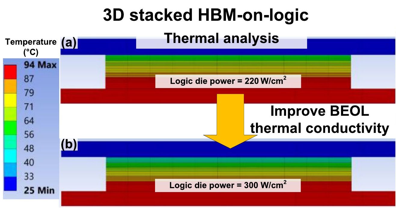
That limit is already shaping chipmakers’ design path for stacked memory. Micron’s vHBM plans, for example, include heat-spreading structures. With HBM stacked on a logic die, and DRAM needing to be kept at or below 95 degrees Celsius, the logic’s heat output is capped at 220 W/cm², or 300 W/cm² with better thermal vias, according to a 2025 simulation by co-founder Shimeng Yu’s group. Nagare Labs says peak compute has grown 70% a year over the past three decades, against 20% for memory bandwidth.
(Image credit: J. Sharda et al., IEEE JxCDC (CC BY 4.0), cropped)
The company describes its Z2RAM as “Two transistors and a shield. No capacitor,” where a write transistor places a charge on a storage node and the shield blocks noisy neighbors. The read transistor can sense without draining. In a gain cell like this, the read transistor’s gate capacitance holds the charge, so reads are non-destructive and the cell avoids DRAM’s write-back. Nagare aims for well under a picojoule per bit.
Nagare builds Z2RAM by depositing its layers on top of the accelerator and patterning them “together on one die,” much as 3D NAND flash scales by adding layers. There’s no interposer and no bonds between the memory layers, which is part of the secret sauce. One lithography exposure covers several layers at once, and standard 300 mm tools with DUV do the job, with no EUV required. The current roadmap is aiming at over 100 layers with “hundreds of thousands” of vertical connections.
Retaining data at higher temperatures is the challenge, and one the founders have probed repeatedly with their testing. A 2020 paper from co-founder Suman Datta’s group, on a tungsten-doped indium oxide two-transistor cell, had retention of 1 second at 25 degrees Celsius and just 300 milliseconds at 85°C. An update in 2025, which has Datta as a co-author, adds a third transistor and removes the gate overlap from its transistors, managing over 1,000 seconds at 25°C, up from 200 seconds with overlapped ones. It also simulated a GPU L2 at twice SRAM’s capacity but in the same area with 75–80% lower energy-delay-area product, a combined score that multiplies energy, delay and area.
Six months later, both founders showed a “folded asymmetric boosted” three-transistor cell that held data for over 300 seconds at 85°C, as compared to only 100 milliseconds for a conventional three-transistor design. That’s still below the roughly 95°C that Nagare says DRAM must stay under, so neither the founders’ published cells nor Z2RAM have shown retention above that line yet. The boosted cell is also “refresh-free,” which means data in the GPU’s last-level cache, profiled from AI workloads, doesn’t have time to decay before it is overwritten.
What the founders’ papers measured and simulated, and what Nagare projects
Physical space is also limited for this application, and the founders project their boosted cell at 0.0168 µm² at 7nm, compared with 0.0199 µm² for a high-density SRAM cell on TSMC’s 3nm (N3) process. A separate study from Yu’s group found that a four-tier, 256MB cache of two-transistor gain cells at 7nm could reach 5.7x the bit density of 7nm SRAM in the same area, in simulation. However, the return on investment falls off past seven or eight tiers because masks scale with layers. Nagare Labs’ claim of single lithography would potentially bypass this limitation.
That has not yet been proven, and nothing published yet shows it. “Where we are is literally lab prototypes,” Datta told The Register, adding that sampling of Z2RAM tiles is targeted within four years and production shipments, if they arrive, within the next decade. Yu told the outlet that no standard yet exists for integrating this kind of memory with an accelerator, which means Nagare might have to come up with the interface itself. Datta also mentioned reliability to the outlet, as single-electron effects can shift a cell’s threshold enough to upset the stored bit. It also remains to be seen if the tested three-transistor cells work sufficiently well as a two-transistor, single-shield product.
Even if Nagare clears those hurdles, a more important one lingers: It currently has no fab. The plan to scale depends on getting partners for fabrication as well as packaging. Nagare is reportedly looking for an R&D fab partner so it can scale beyond the university clean room. Perhaps the most similar type of memory-on-compute shipping today, and the one Datta cited to the outlet as a model for working with chipmakers, is AMD’s 3D V-Cache.
Z2RAM isn’t the first capacitorless memory to promise a 5x improvement over SRAM in density; it follows in the footsteps of Innovative Silicon’s Z-RAM from 20 years ago, a technology AMD licensed, though it was not pursued. A Georgia Tech paper due at IEDM in December covers a different device, a one-transistor, one-ferroelectric-transistor cell, aimed at the same gap between SRAM latency and DRAM density.
Gelsinger, previously CEO of Intel, which started as a memory company, phased out Optane, a low-latency non-volatile memory, in favor of CXL. Optane sought to bridge the gap between slower non-volatile storage, such as HDDs and standard SSDs, and DRAM. Now he sits on Nagare’s board, and Playground Global, where he is a general partner, led the startup’s $5 million round as Nagare searches for a solution to a different but related problem.
Nagare declined to share measured retention, latency, or energy figures. The founders’ boosted cell already holds data at 85°C longer than a cache needs, but until a fab-built, multi-layer Z2RAM stack is measured, retention above 95°C included, its headline numbers remain projections.
AI creator Nick Saraev says on X that Amazon closed his account after he tried to buy seven Nvidia DGX Spark AI mini-PCs. The closure email cites a verification process and gives no reason. Epic CEO Tim Sweeney chimed in that his regular orders would go through, then get canceled before arrival, after he tried to buy two GPUs.
Update: Amazon just closed my account.Buying even modest amounts of compute immediately puts you on a watchlist. Be careful!November 1, 2026
Saraev puts it plainly that “Amazon just closed my account” and that “Buying even modest amounts of compute immediately puts you on a watchlist.” He was “4 orders deep,” and Amazon will no longer allow him to buy DGX Sparks.
The shared screenshots indicate those orders were all canceled, with each stating, “Your order was canceled. You have not been charged for this order.” Although he does not give a unit count, the screenshots indicate he tried to buy seven DGX Sparks in total. All show the same listing, with 128GB of memory and 4TB of storage.
Amazon’s support account did respond to his earlier post, about three hours before his closure post, offering a review. The shared email shows that Amazon had “made the final decision” to close his account after review; no reason was given. However, it did mention “previous attempts to verify your account,” and he says he did go through the verification process, but seven DGX Sparks is a significant amount that might draw suspicion. Either way, Amazon’s Conditions of Use reserve the right to “refuse service, terminate accounts” or “cancel orders in its sole discretion.”
He’s not alone in running into trouble with the company. Sweeney says that “Amazon didn’t cancel my account but continued accepting all my regular orders and canceling them just prior to arrival dates, after I tried to buy two NVIDIA GPUs. Rather bizarre.” Nvidia GPUs are often used for local inference. Saraev replied that everyone would “appreciate a bit more transparency.”
Also, in September, Dracones89 on the Nvidia developer forum shared that one Amazon account was hit with “suspicious activity locks” while trying to buy a pair of Asus GX10s; the user ended up with two DGX Sparks from Micro Center instead. Another X user, @PurzBeats, wrote, “They canceled the order when I tried to buy my 5090, twice.” This is a different trajectory than the OpenClaw days of Mac minis, when buyers faced long delivery waits rather than canceled orders or closed accounts.
With local inference remaining of high interest to many, particularly AI influencers, the event is potentially disturbing, especially after recent comments about self-owned DRAM by OpenAI CEO Sam Altman. While this time it was a guy who helps entrepreneurs and small businesses implement AI and claims 500K on YouTube and 700K on Instagram, the slope is slippery, although Saraev’s orders are hardly typical.
The 128GB DGX Spark has an MSRP of $6,950, but it may be found at 20% or more over that: two Amazon listings showed $8,499.99 and $9,499.99 when we checked today, which would put seven at roughly $59,500 to $66,500. Both showed Prime delivery tomorrow, so the hardware is still on sale there.
Hardware has been climbing in price, largely due to rising memory costs. As open-weight models have become more popular, so has local AI inference. The combination may make retailers uneasy, as you’re dealing with high ticket prices and there has been uncertainty about the safety of models as they have improved, with open-source AI agent tools reportedly being used in multiple recent cybersecurity incidents.
Micro Center, a different retailer, required one buyer to sign an Advanced Computing Product Purchaser Declaration with photo ID, end user, and an install location, just for a workstation with an RTX 5090. This form specifically forbade exporting or reselling the hardware, which might give a little insight into Amazon’s reasoning, too. Amazon’s conditions also say customers “must comply with all U.S. or other export and re-export restrictions.” China and the U.S. remain locked in a fight over exports of AI hardware.
Amazon hasn’t explained itself, but the attention this is getting may motivate a more detailed response. Right now, it’s a warning signal to users looking to buy significant amounts of hardware for AI work, at least from traditional online retailers. Brick-and-mortar stores, like Micro Center, may crack down further to prevent workarounds designed to export the hardware illegally.
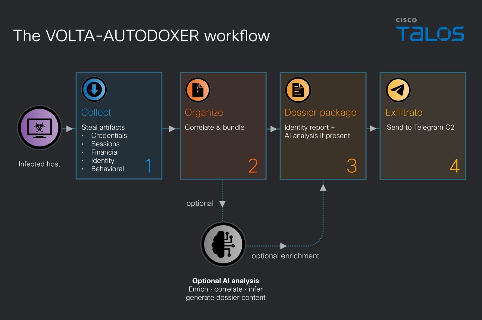
A self-deleting Windows infostealer that calls itself VOLTA-AUTODOXER steals everything it can from a victim’s PC, then asks an AI model, Anthropic’s Claude by default, to turn the haul into a target assessment, Cisco’s Talos research organization reports. The malware builds a structured “evidence bundle” on the person and asks the model for a list of their valuables ranked by how much they could be cashed out for, to see what’s worth the effort. VOLTA operates with a prompt to act as “a forensic intelligence analyst” and to be “blunt, specific, accurate,” and can switch models if one refuses, or even do without.
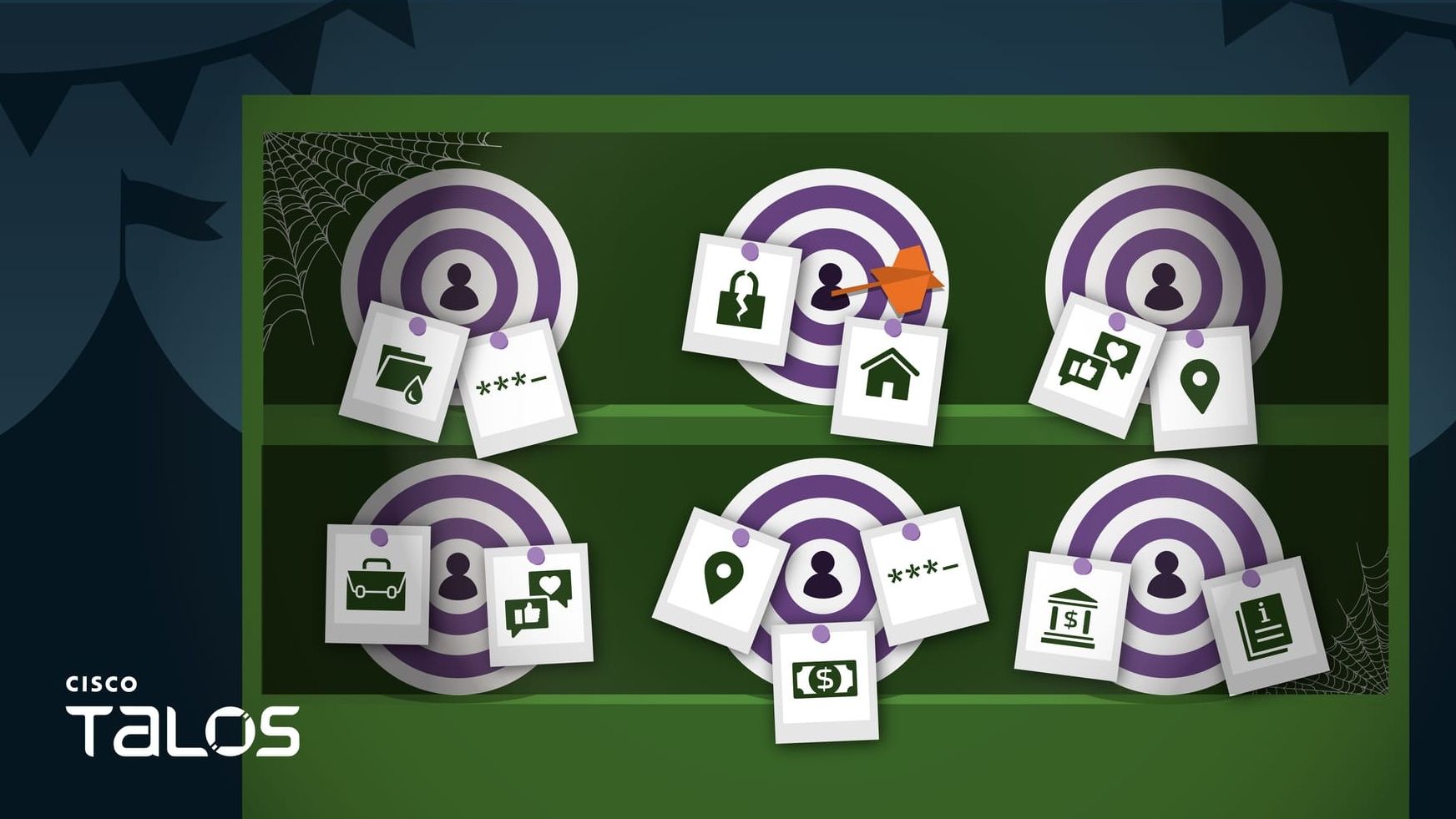
VOLTA steals browser passwords, cookies, and saved payment cards, Thunderbird and Outlook email profiles, Roblox accounts, Microsoft OAuth tokens, screenshots, and even SSH and cloud-provider configuration files. Every saved Wi-Fi password gets pulled in plaintext. Cryptocurrency wallets, when present, are not just copied, as the malware attempts to crack their vaults inline. It then builds the evidence bundle on the person: geolocation and home address, employer and employer domain, inferred birth year, document authorship metadata, and the last four digits of their payment cards.
It also engages in live enrichment with any stolen sessions. VOLTA searches the victim’s Gmail for receipts from Amazon, DoorDash, Uber Eats, Grubhub, Walmart, and PayPal to confirm a home address, pulls Uber Eats and DoorDash order histories, reuses the stolen Discord token to fill in the victim’s profile, and values Roblox items through Rolimons. The theft list is relatively standard for a stealer, but this enrichment pass turns passive data into something dangerous.
The data is first assembled locally as Identity_Report.txt and serialized to JSON, before being POSTed to OpenRouter, a popular model router, with the system prompt. Any reply is saved as AI_Analysis.txt, and both are exfiltrated together in a volta_dox.zip archive file. This inference call happens over the victim’s own network connection. The model call asks for a concise assessment of the victim’s suitability as a target, backed by citations, with “opsec” to analyze overall security posture, including password hygiene.
The settings in use include Anthropic’s Claude Opus 4.6 by default, an older model released in February, at a temperature of 0.2. Temperature controls how random a model’s output is from a baseline 1.0, and the hardcoded low value suggests the operator prioritizes predictability. The author likely anticipates refusals, and VOLTA looks for refusal phrases and thin replies, switching to two other models, Moonshot AI’s Kimi K2 and Google’s Gemini 2.5 Flash, in that order. If the VOLTA user supplies no API key for OpenRouter, it can still send the dossier over Telegram without the AI data.
VOLTA appears to be a product designed for resale, as it has a template with six swappable slots — for a custom Telegram channel, API keys, and settings — that are filled at build time. The customer would supply the values, and a custom binary would be created. While the slot credentials are encrypted, it’s possible to recover them from the file. Assuming everything goes to plan with the delivered build, the customer receives ranked target assessments in their Telegram inbox without relying on any attacker-owned infrastructure; the chokepoints are on the services.
Much of the token theft relies on bypassing Chrome’s App-Bound Encryption (ABE), which VOLTA does by launching Chrome headless, that is, without a GUI. An application-control policy that limits which processes may launch Chrome headless blocks the ABE decryption path. This reduces exposure to VOLTA’s particular method of attack by denying it access to Chrome-stored sessions, but it doesn’t stop its other theft, the AI stage, or exfiltration.
After infection, the main executable may delete itself, but a volta_debug.txt file should be preserved by the victim. This file is a log that shows what was collected and whether the LLM call was successful. The target should revoke or rotate all API keys and tokens and change passwords, regardless of exposure; likewise, any funds in a wallet whose seed phrase was stored in plaintext should be moved to a new wallet with a fresh seed, preferably generated on an air-gapped device.
One very real concern is that VOLTA’s use of AI is relatively narrow compared with what is possible with fully AI-assisted malware, especially as models could be utilized for additional phases. Refusal resilience may become a standard design requirement for malware as AI integration matures. Already, a Windows malware implant reported in September was built around a panel of up to four LLMs that vote on its next move, and another, reported this week, can fall back to using the victim’s own OpenAI API key. This is still a process of having AI replace the work a human analyst would normally do, so the real question is which stage is next.
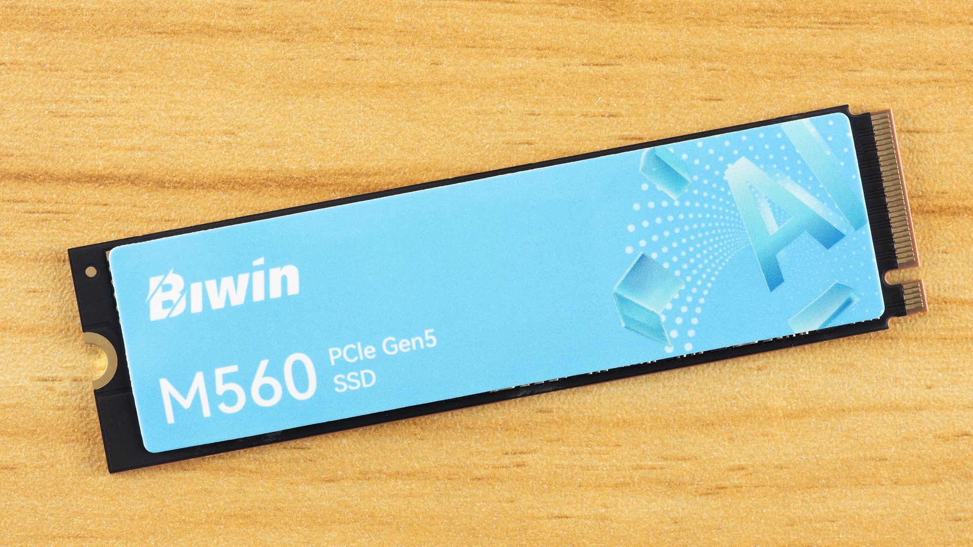
We’re back with another drive from Biwin, which has been putting out some good SSDs with minor exceptions. This one uses hardware we’ve wanted to test in retail for quite some time: the SMI SM2504XT SSD controller, which is hard to find. The PCIe 5.0 DRAM-less range is relatively popular because it offers the performance without the power and heat of higher-end options, at a lower price point. The tech’s newer than what PCIe 4.0 drives offer, so you get a better all-around experience if you’re willing to take the plunge. The M560 slots in here perfectly as a real alternative to all the drives in this class with Phison hardware.
Biwin M560 Specifications
Product
1TB
2TB
Pricing
$189.99
$364.99
Form Factor
M.2 2280 (Single-sided)
M.2 2280 (Single-sided)
Interface / Protocol
PCIe 5.0 x4 / NVMe 2.0
PCIe 5.0 x4 / NVMe 2.0
Controller
SMI SM2504XT
SMI SM2504XT
DRAM
DRAM-less / HMB
DRAM-less / HMB
Memory
218-layer BiCS8 TLC (Kioxia)
218-layer BiCS8 TLC (Kioxia)
Sequential Read
11,000 MB/s
11,000 MB/s
Sequential Write
9,700 MB/s
10,000 MB/s
Random Read
1,400K
1,700K
Random Write
1,600K
1,700K
Security
N/A
N/A
Endurance (TBW)
750TB
1,500TB
Part Number
BM560NN01TB-RGX
BM560NN02TB-RGX
Height
2.45 mm
2.45 mm
Warranty
5-Year
5-Year
The Biwin M560 is available only in 1TB and 2TB capacities. Is that a disappointment? It’s normal to expect at least 4TB SKUs these days, but 8TB is certainly a bridge too far for a four-channel controller. Yes, we have some 8TB DRAM-less drives floating around, but for the most part you can’t find those units. 4TB is more common and highly desired — this is what makes the Lexar NM790 so legendary — but it actually is a decent amount of flash for this type of controller. With the ideal amount of flash for this controller being four dies per channel, or 16 total, 2TB really is the sweet spot. So we’re fine with that for this drive, even if it is higher-end.
Right now the drive can be found for $189.99 and $364.99 for the two SKUs, which is not unreasonably priced for the hardware. At 2TB, it is right in line with the Crucial P510, for example. It’s also below the top drives with DRAM, like the Samsung 9100 Pro, by enough that it makes sense. You can get PCIe 5.0 DRAM SSDs at around this price or cheaper, but you’re giving up some things to do so, which we’ll get into later.
The drive is rated for up to 11,000 / 10,000 MB/s for sequential reads and writes and up to a whopping 1,700K / 1,700K random read and write IOPS. 1.7 million IOPS! That’s astounding, and even exceeds the 1.3+ million, on paper, from direct competitor Phison E31T-based drives, like the Corsair MP700 Elite. This thing is a beast for a DRAM-less drive.
Biwin doesn’t skimp on the warranty, either. It’s the typical five-year affair for duration, but you’re covered for up to 750TB of writes for every TB of space. This is 25% more than is typical, if you care about that sort of thing. We consider it a bonus.
Biwin M560 Software and Accessories
Hitting the download tab for the M560’s site shows three downloads available: the Biwin Data Recovery Tool for macOS, one for Windows, and Biwin Intelligence. The first two are pretty self-explanatory, but we will give kudos to Biwin for having the macOS option. For the last, it is the company’s SSD toolbox, which is an all-in-one software solution dashboard you can use to check your drive’s health, update firmware, and so forth. Biwin lists the supported functions on its page. The toolbox only supports Windows at this time.
Biwin M560: A Closer Look
Tom's HardwareTom's Hardware
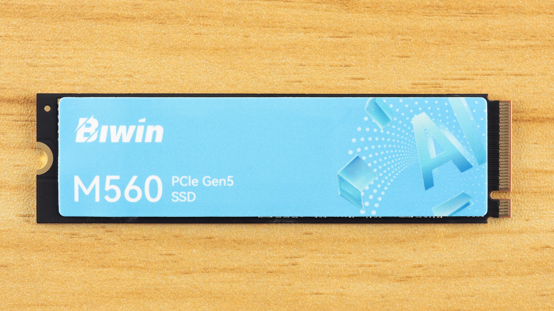
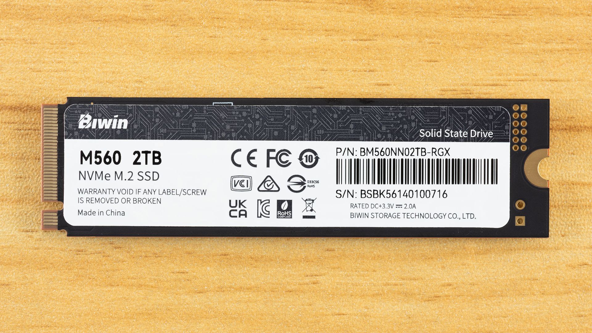
The Biwin M560 is, as expected, a single-sided drive, which we prefer. Less that can go wrong, fits into more machines, and can be easier to cool. The top label is heat-spreading. The back label has drive information, including the 3.3 V / 2.0 A rating, which puts the drive power draw below about 7W. According to the S.M.A.R.T. report, the maximum power draw is 8W.
These numbers might be concerning, especially as good DRAM-less SSDs tend to be at around 6.5W or less. Well, as it turns out, the drive is much more comfortable at 4W, with a maximum significantly below 6.5W and an average of one-half that, as you can explore in more detail with our power testing. Even very efficient PCIe 5.0 drives tend to step up over the last generation, making heat something to watch in some cases. Not in this one — we think this will be great in laptops, and exceptionally cool in PCIe 4.0 ones.
Tom's HardwareTom's HardwareTom's Hardware
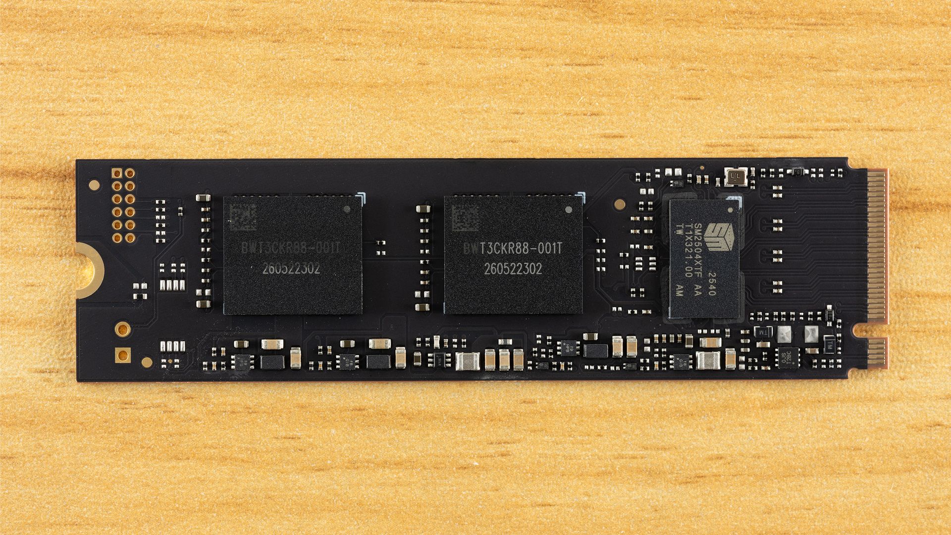
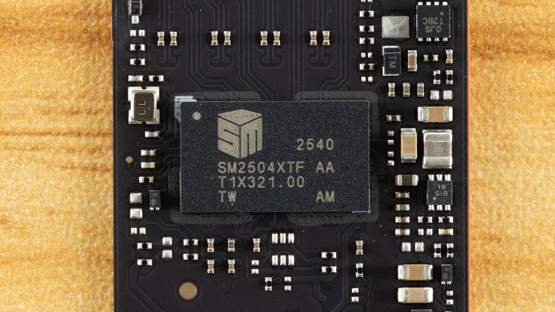
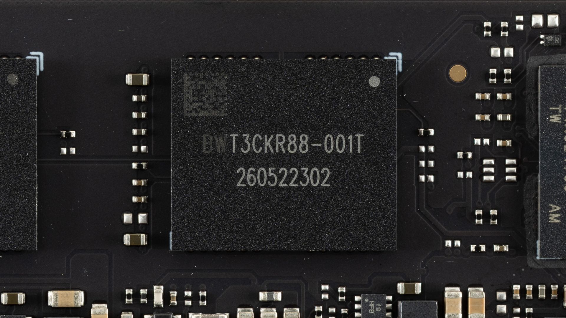
The components don’t even take up half of the PCB space! Impressive engineering, and the extra spacing between components can help spread heat. Here we have one controller, the SMI SM2504XT, which we previously covered in an ES preview, and two NAND flash packages. The controller performed exceptionally in our preview testing and is more than a match for the best controllers out there, whether Phison’s competing E31T or even many drives with DRAM such as those based on the E26. The flash, in this case, is Kioxia’s 218-layer BiCS8 TLC, which is also exceptional. This flash has excellent latency and is also power-efficient. This combination is a match made in heaven, and it’s a shame we don’t see the SM2504XT more often.
We considered pitting the Biwin M560 against some truly high-end drives, but truth be told, we don’t think that’s a valid comparison. If you’re someone who wants DRAM and maximum bandwidth — that means eight flash channels — then this drive is not going to cut it, even if it performs like it does. On the other hand, you may legitimately want a drive in this range that isn’t going to burn your house down. That’s closer to what we’re looking at here. We did throw in the PCIe 4.0 Kingston NV3 for good measure, since it’s using SMI’s comparable controller of that generation, but we suspect that if you’re looking at PCIe 5.0 drives, you are not going to settle for anything less.
To that end, we have direct competitors with Phison’s E31T controller: the Addlink G55, the PNY CS2150, the Corsair MP700 Elite, and the Crucial P510, the last of which has Micron rather than Kioxia flash. We’ve thrown in the SM2504XT ES to show any differences against the more mature M560. We also have a higher-end DRAM-less drive in the Biwin Black Opal X570, which has eight channels. We also have the Crucial T700, which doesn’t break the DRAM and bandwidth rule because, for one, it’s using the older Phison E26 controller and, for two, it’s not the full 14 GB/s variant. There are 10 GB/s drives using that controller, but we think the 12 GB/s T700 is the most appropriate comparison.
Trace Testing — 3DMark Storage Benchmark
Built for gamers, 3DMark’s Storage Benchmark focuses on real-world gaming performance. Each round in this benchmark stresses storage based on gaming activities including loading games, saving progress, installing game files, and recording gameplay video streams. Future gaming benchmarks will be DirectStorage-inclusive and an evaluation for future-proofing is included where applicable.
Tom's HardwareTom's HardwareTom's Hardware
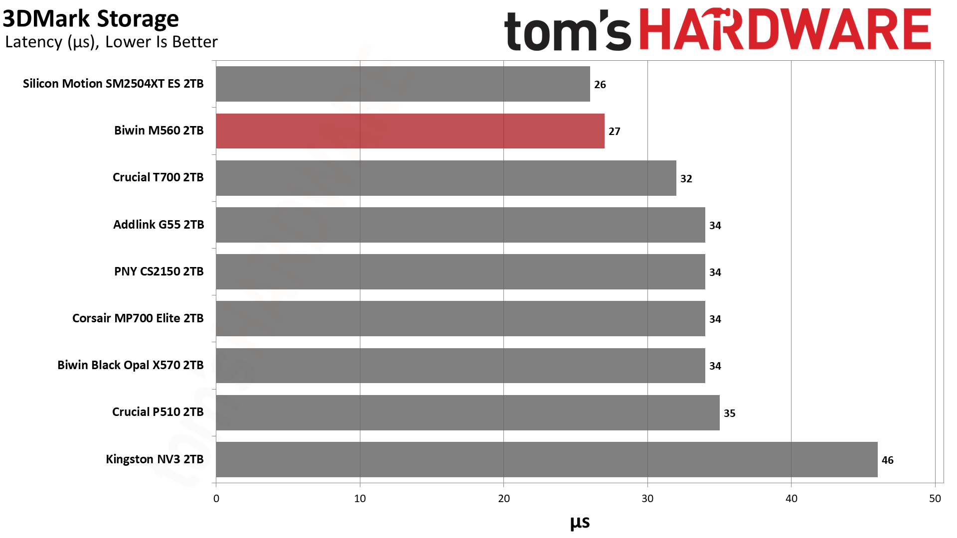
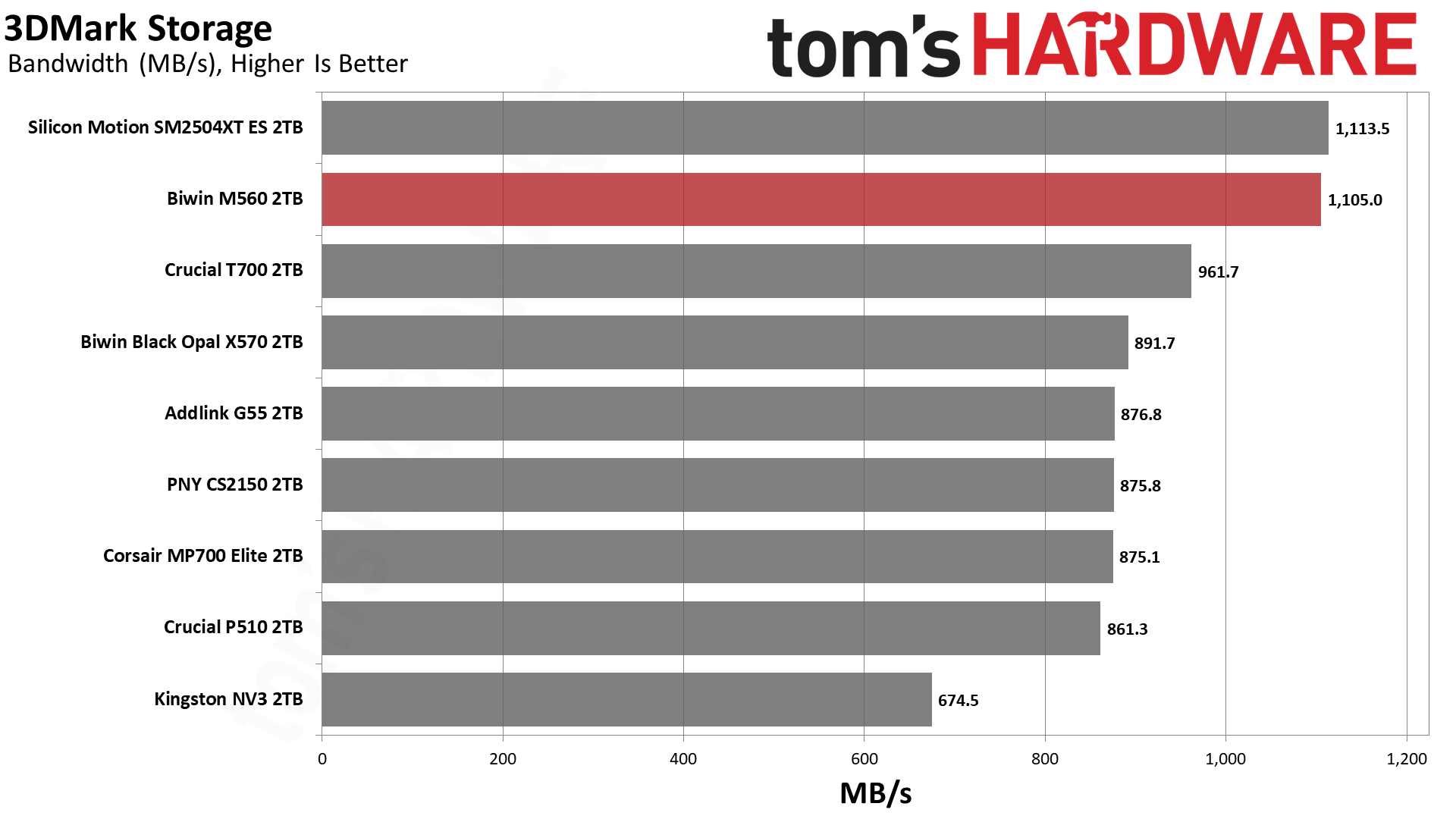
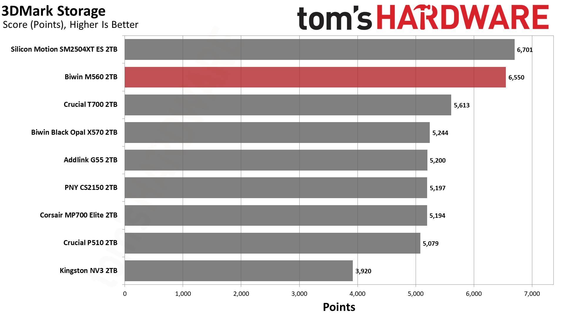
You love to see it: the M560 blows the doors off this benchmark. It comes second only to the ES but, for all intents and purposes, it’s well above any of the competition. This flash is exceptional, but clearly the controller makes the difference here. There are faster high-end drives like the WD Black SN8100, but that uses BiCS8 TLC and an SMI controller, too. This is an SM2508 “Mini-Me,” which is perfect if you want a fast drive without the baggage of a top-end drive.
Trace Testing — PCMark 10 Storage Benchmark
PCMark 10 is an industry standard trace-based benchmark that uses a wide-ranging set of real-world traces from popular applications and everyday tasks to measure the performance of storage devices. The results are particularly useful when analyzing drives for their use as primary/boot storage devices and in work environments.
Tom's HardwareTom's HardwareTom's Hardware
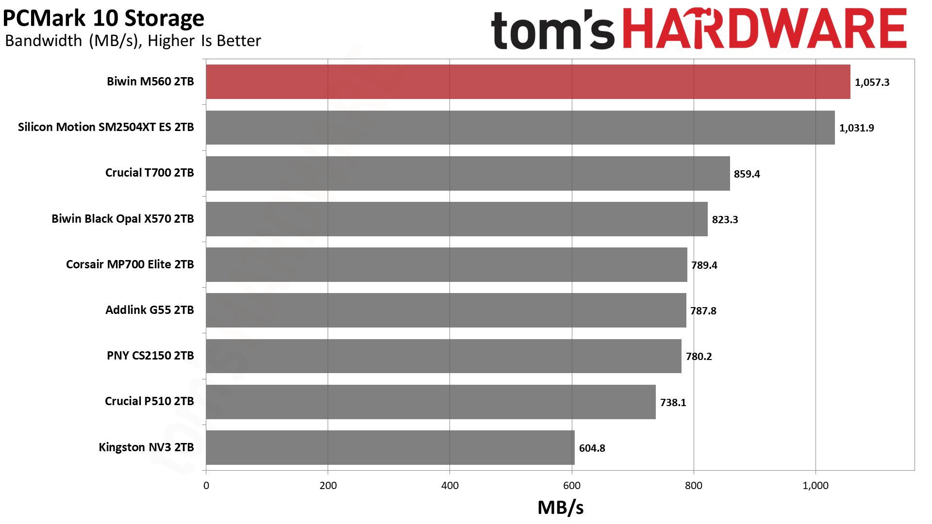
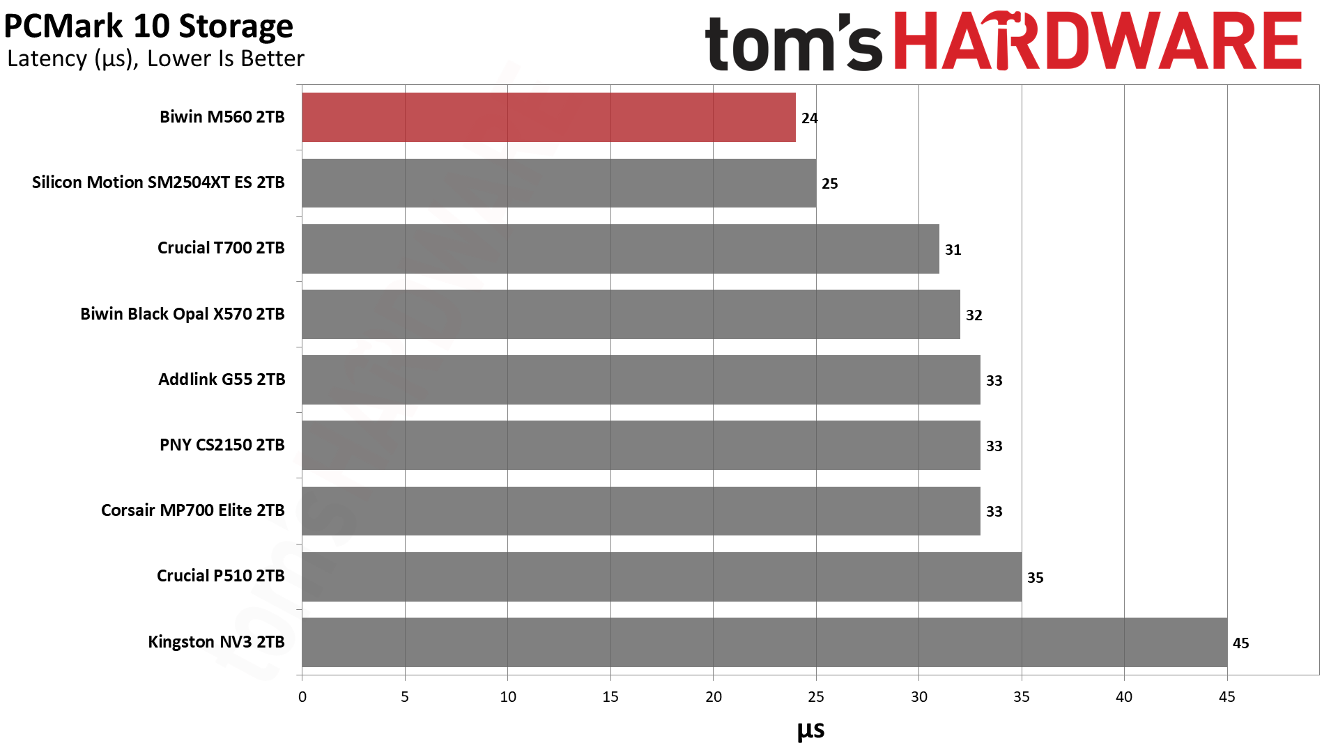
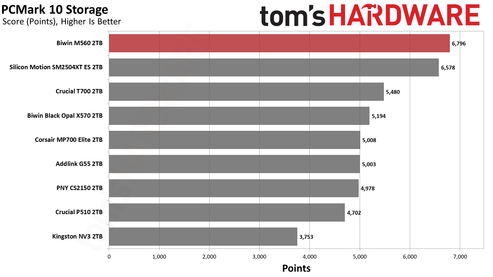
The M560 and SM2504XT ES switched places this time, with the Biwin drive ending up in first place. It’s well ahead of the other drives, with almost half the latency of the NV3. This is an extremely responsive SSD that’s not too far off from the very best, finishing in the top ten of all drives we’ve ever tested.
Console Testing — PlayStation 5 Transfers
The PlayStation 5 is capable of taking one additional PCIe 4.0 or faster SSD for extra game storage. While any 4.0 drive will technically work, Sony recommends drives that can deliver at least 5,500 MB/s of sequential read bandwidth for optimal performance. Based on our extensive testing, PCIe 5.0 SSDs don’t bring much to the table and generally shouldn’t be used in the PS5, especially as they may require additional cooling. Check our Best PS5 SSDs article for more information.
Our testing utilizes the PS5’s internal storage test and manual read/write tests with over 192GB of data both from and to the internal storage. Throttling is prevented where possible to see how each drive operates under ideal conditions. While game load times should not deviate much from drive to drive, our results can indicate which drives may be more responsive in long-term use.
Tom's HardwareTom's HardwareTom's Hardware
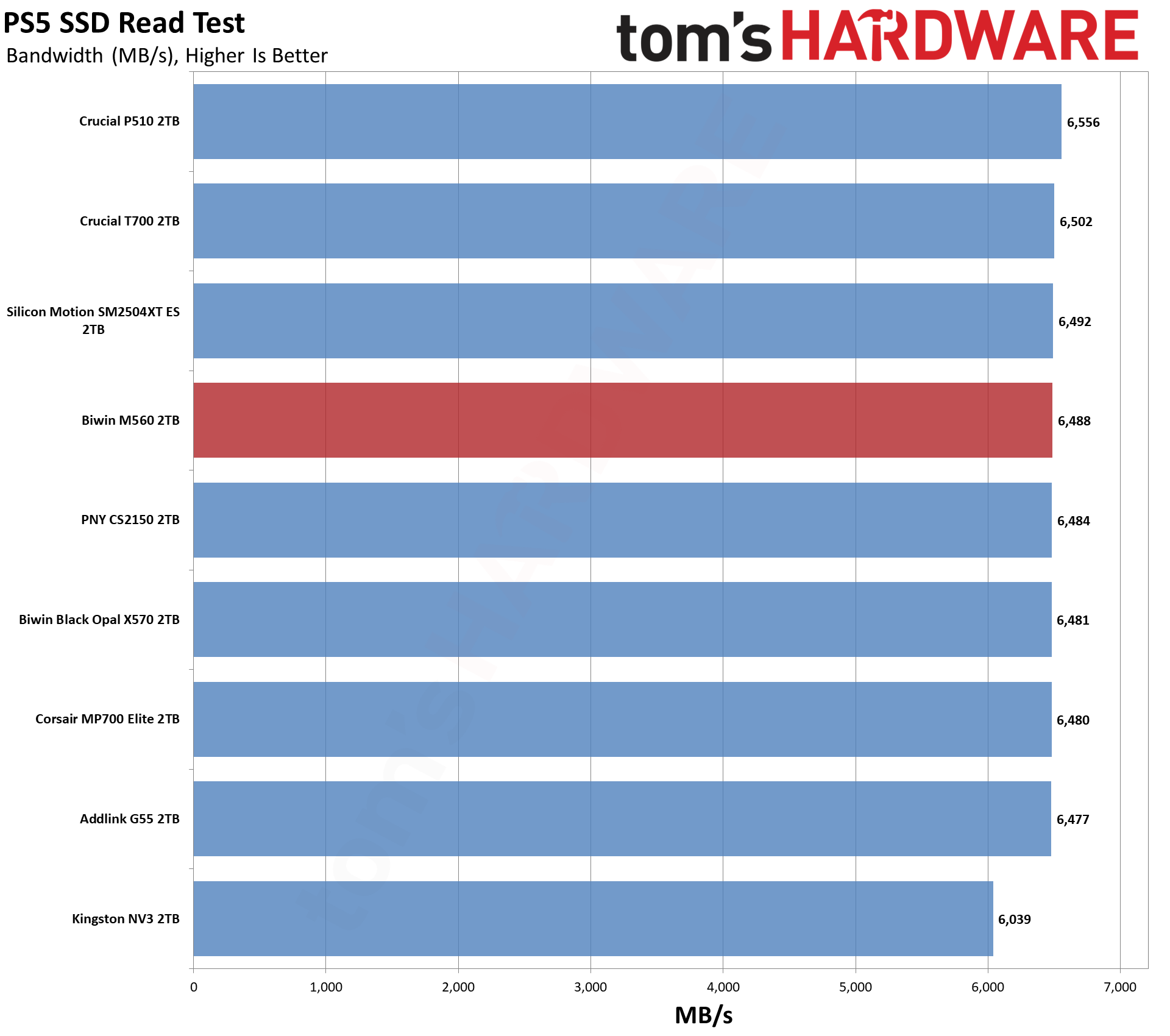
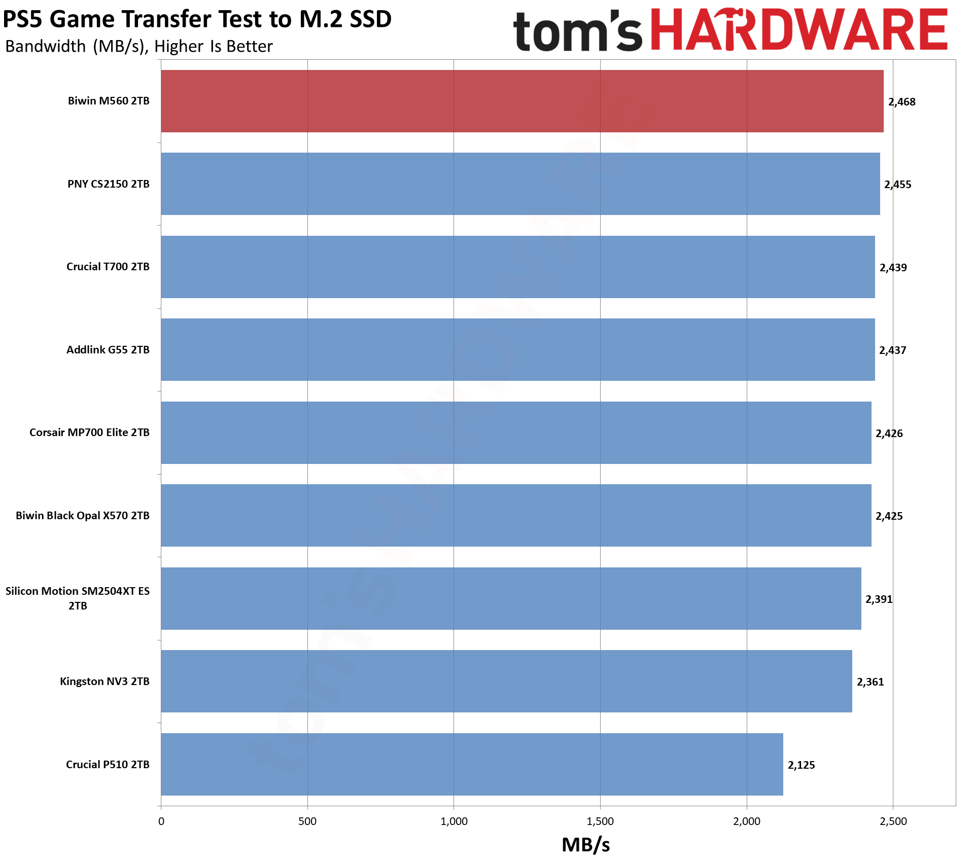
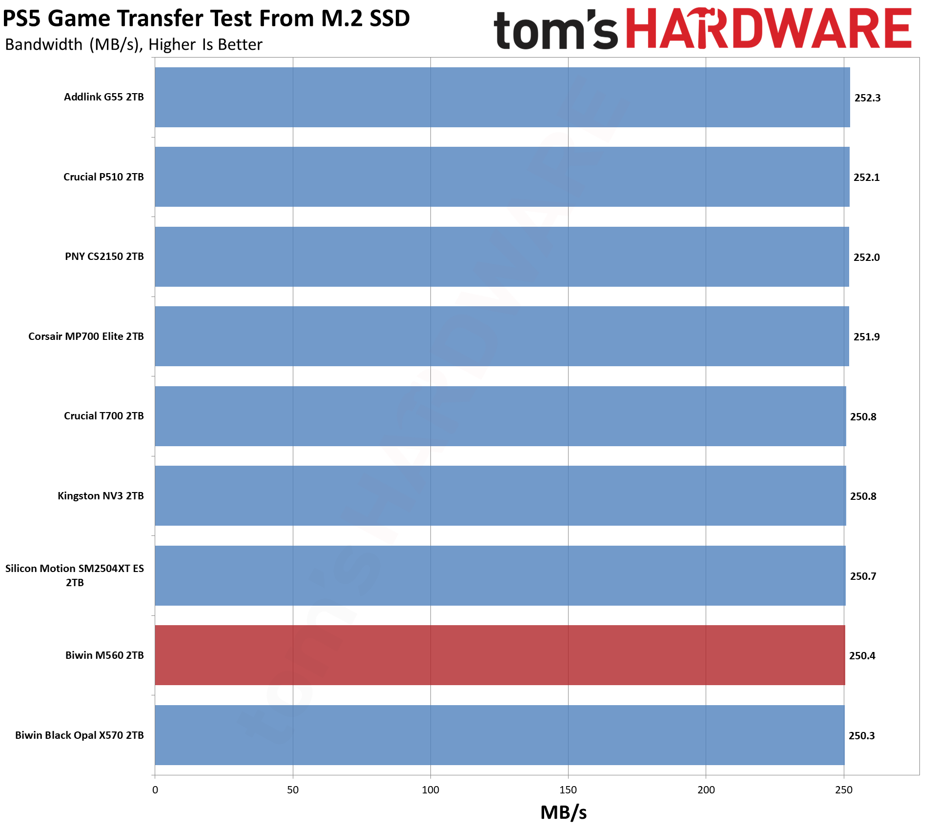
The PS5, why not? The M560 has good results here, as expected, even if it is overkill. We can still recommend it, as it’s going to run very cool at PCIe 4.0 speeds. We think you’re usually better off with a 4TB PCIe 4.0 drive like the Addlink A93, pound for pound, but this one would work.
Transfer Rates — DiskBench
We use the DiskBench storage benchmarking tool to test file transfer performance with a custom 50GB dataset. We write 31,227 files of various types, such as pictures, PDFs, and videos to the test drive, then make a copy of that data to a new folder, and follow up with a reading test of a newly written 6.5GB zip file. This is a real-world type workload that fits into the cache of most drives.
Tom's HardwareTom's HardwareTom's Hardware
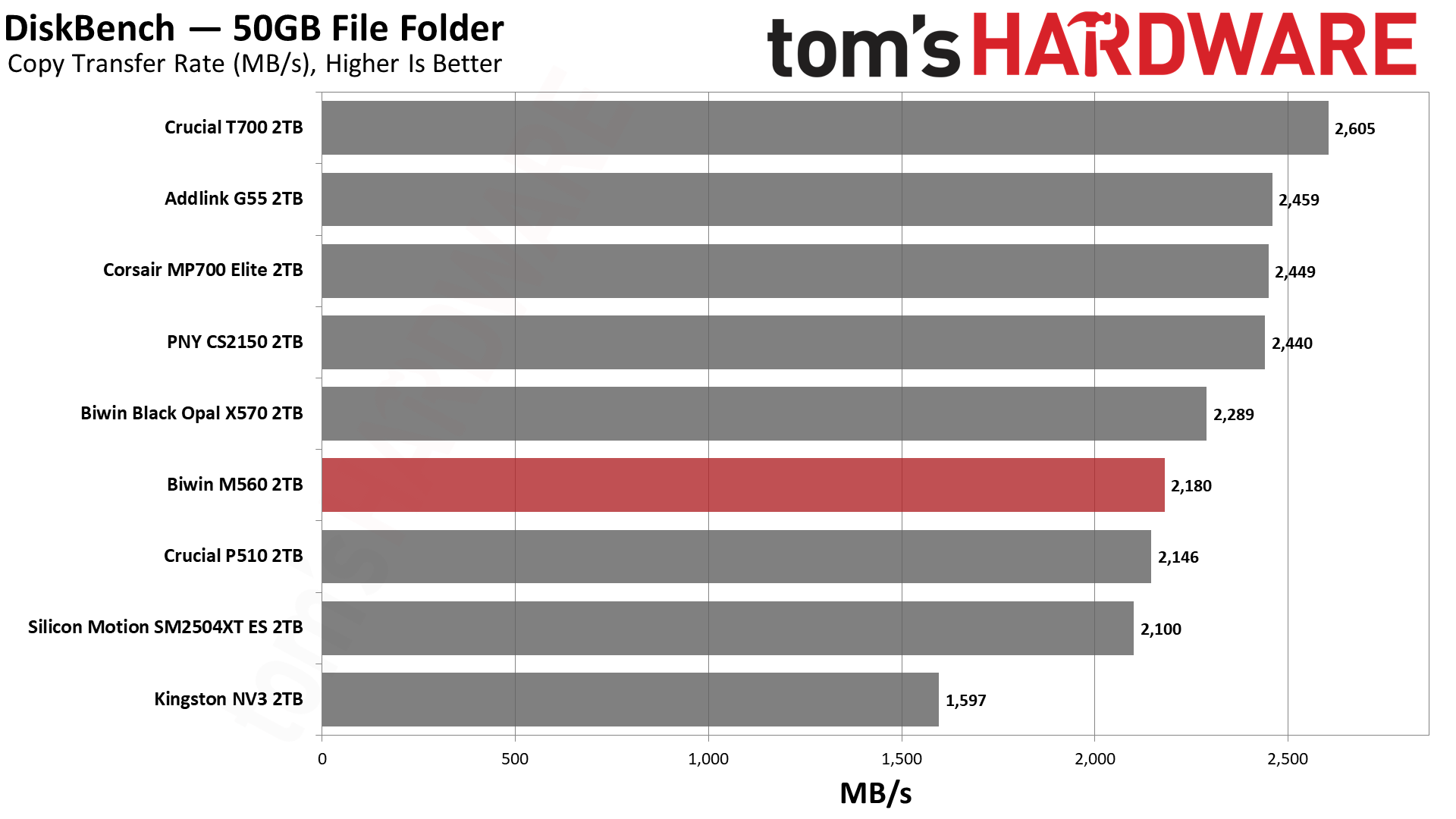
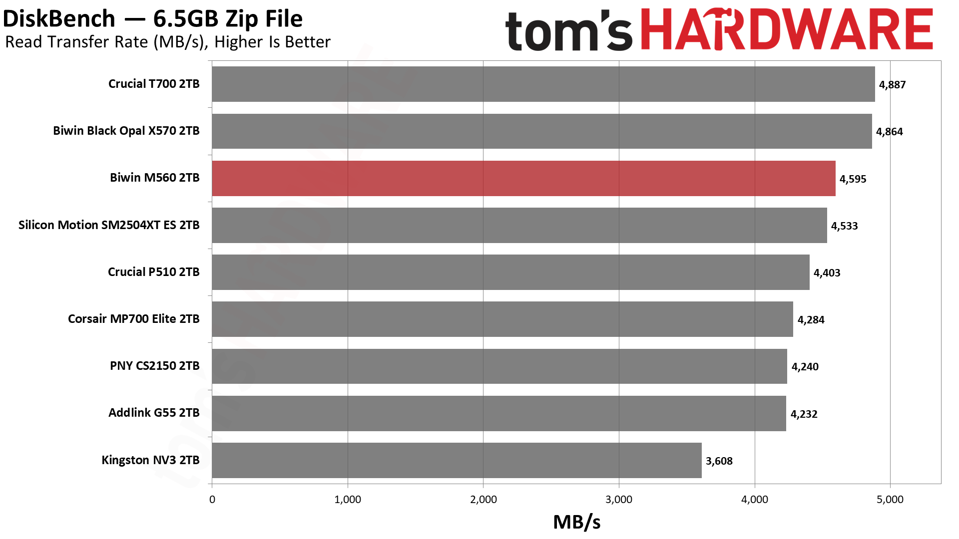
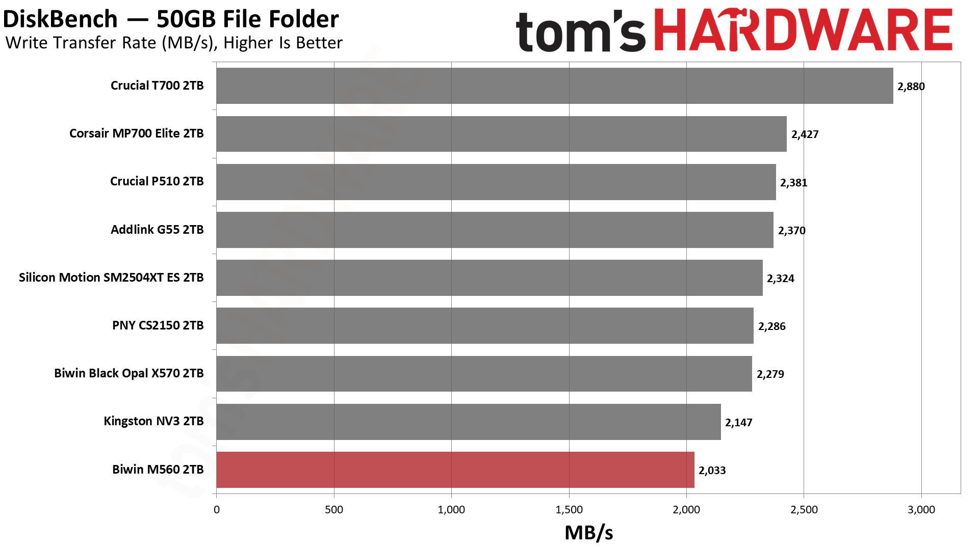
This is the one less impressive test for the drive, and it’s not unexpected, as the SM2504XT also fared somewhat poorly here. The M560 beats it at copying and reading, but not at writing. For copying, it also gets ahead of the P510, which, in our opinion, isn’t bad. Phison’s controller with BiCS8, with the CS2150, MP700 Elite, and G55, is just faster. We can’t chalk this up to a bandwidth difference or a latency difference, so our best guess is that the SMI controller is just not as well-optimized here.
Synthetic Testing — ATTO / CrystalDiskMark
ATTO and CrystalDiskMark (CDM) are free and easy-to-use storage benchmarking tools that SSD vendors commonly use to assign performance specifications to their products. Both of these tools give us insight into how each device handles different file sizes and at different queue depths for both sequential and random workloads.
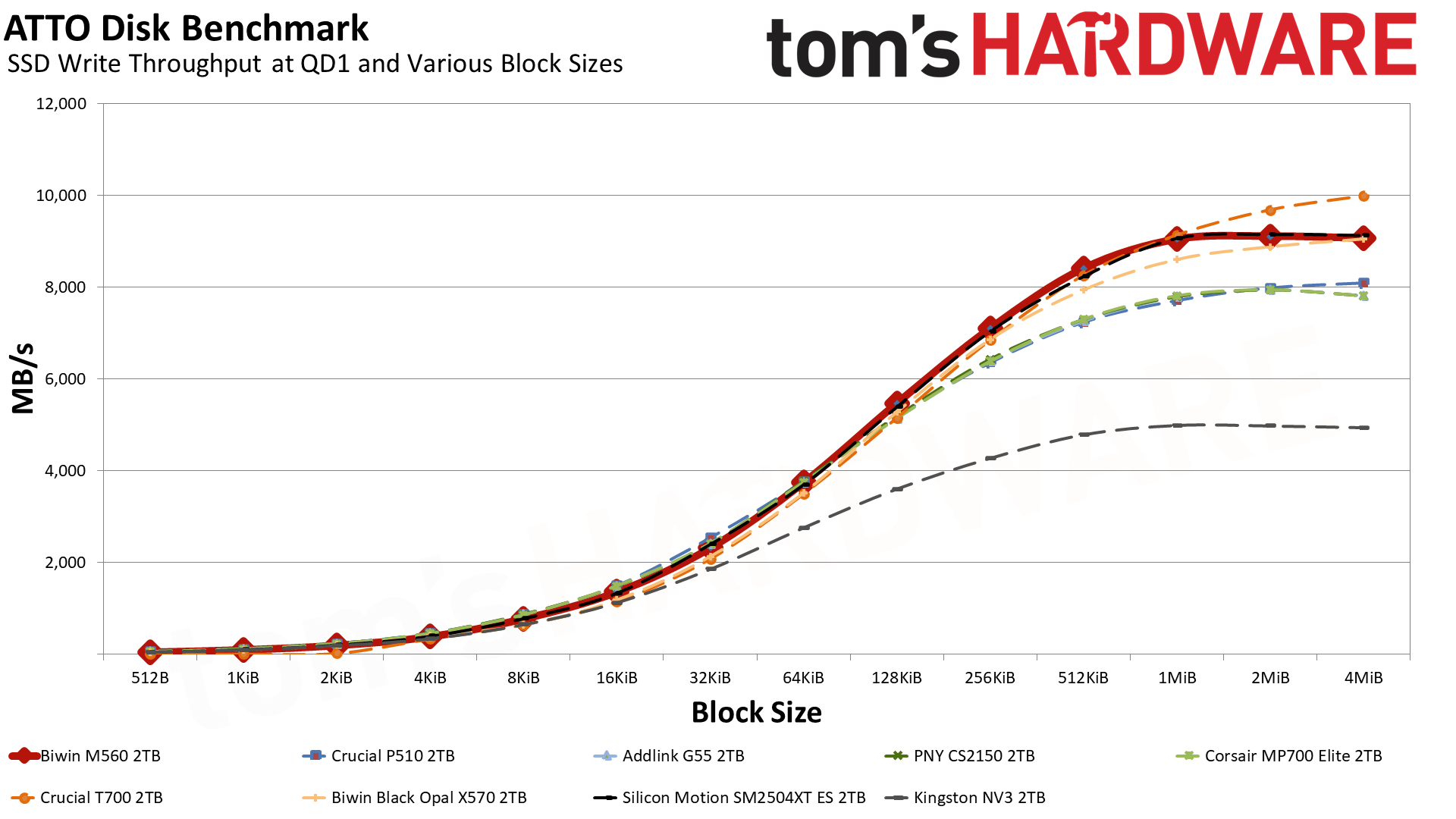
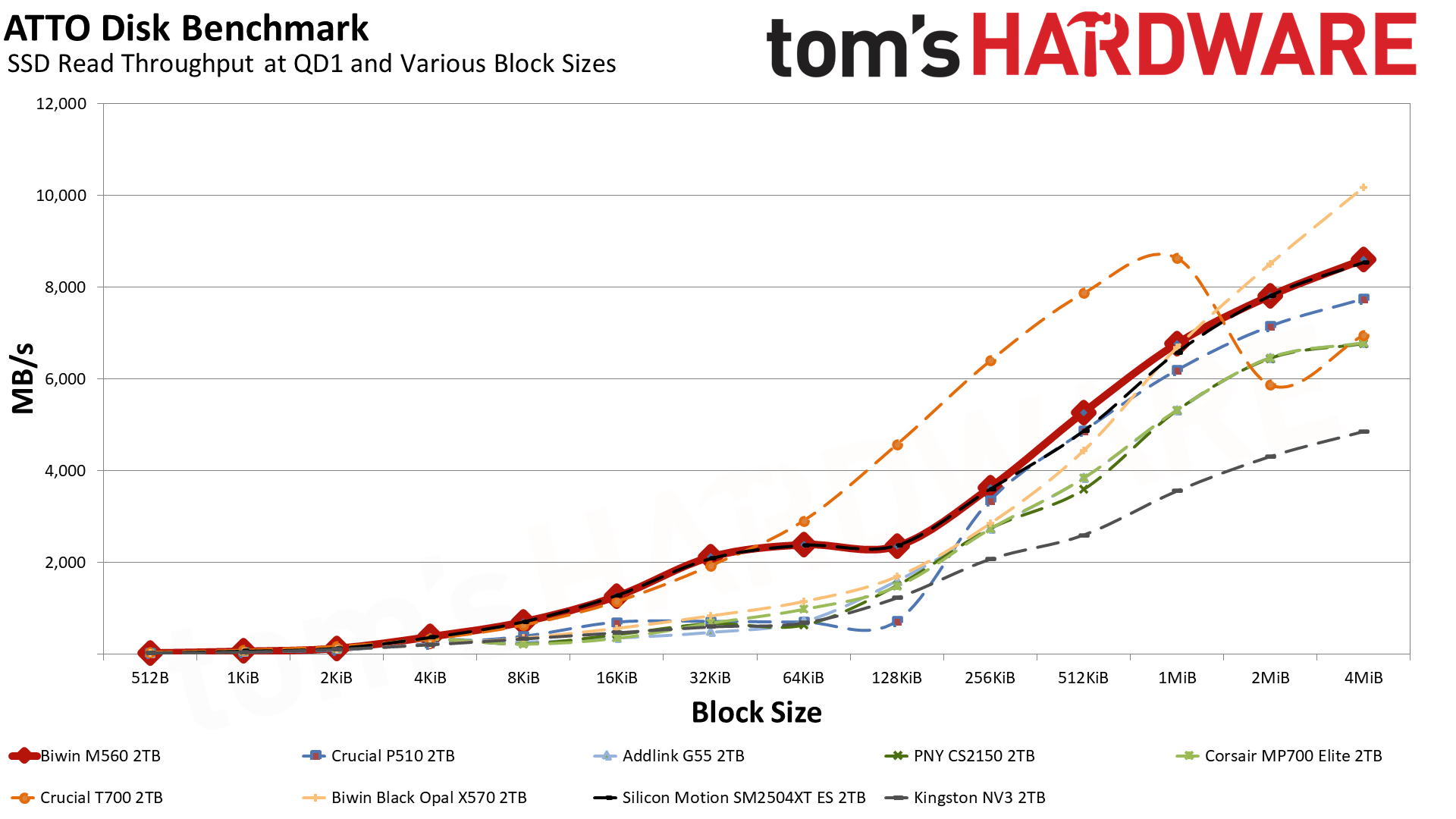
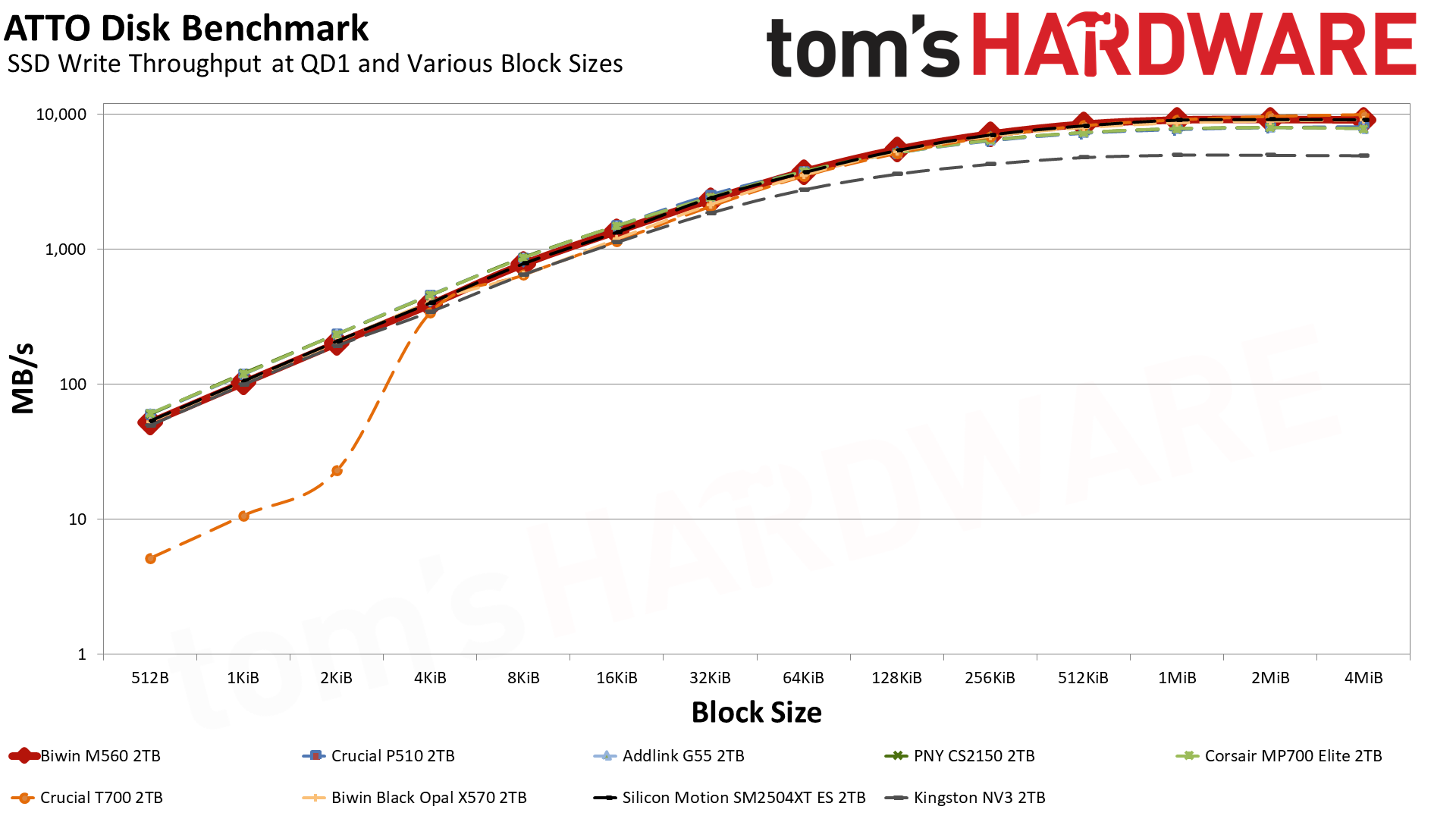
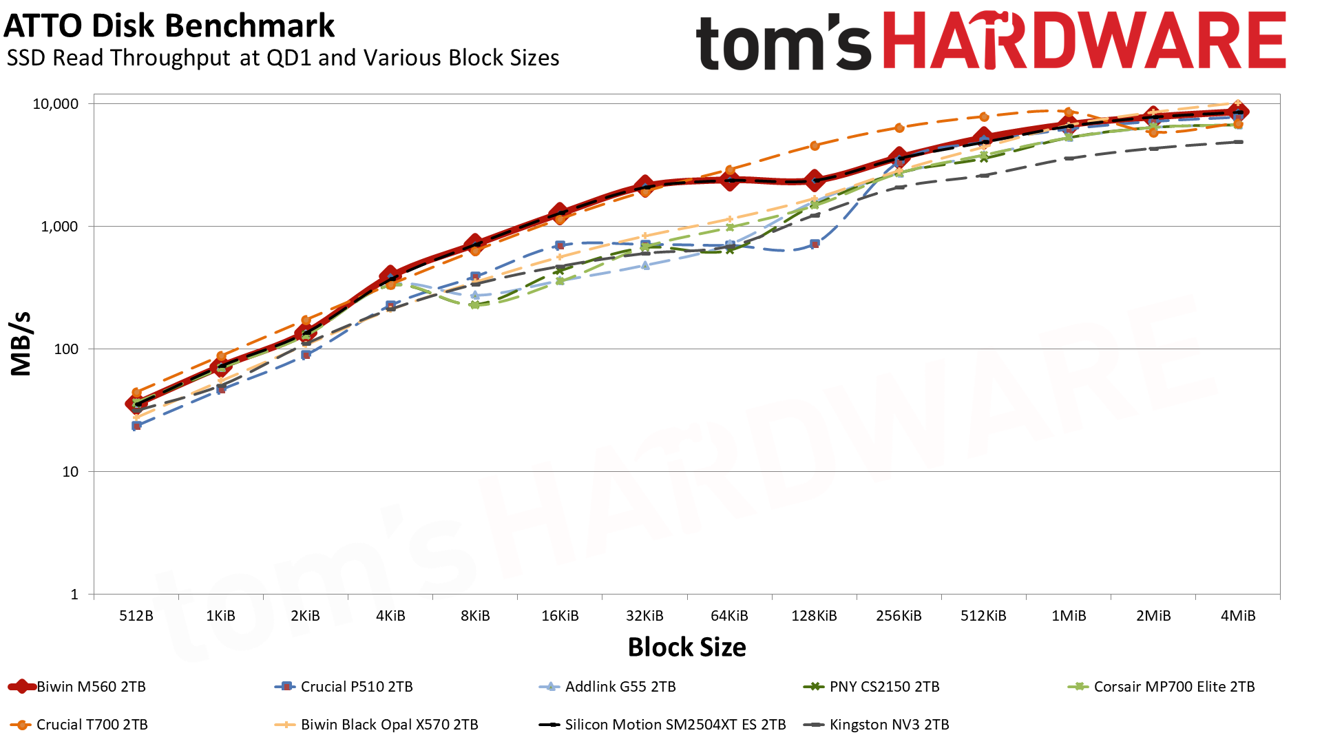
Let’s start with ATTO. For writes, the M560’s curve is quite nice, and it only loses to the T700 — which has double the flash channels, DRAM, and a higher bandwidth ceiling — at the largest block sizes. It even mostly outdoes the eight-channel X570 that’s rated for 10 GB/s with sequential writes. Reads are more of a mixed bag, but in general it’s better than any other drive except for the T700, which it defeats at 2 MiB and up, and the X570, which beats it in that same range. Effectively, this makes the M560 a monster drive for its class any way you slice it.
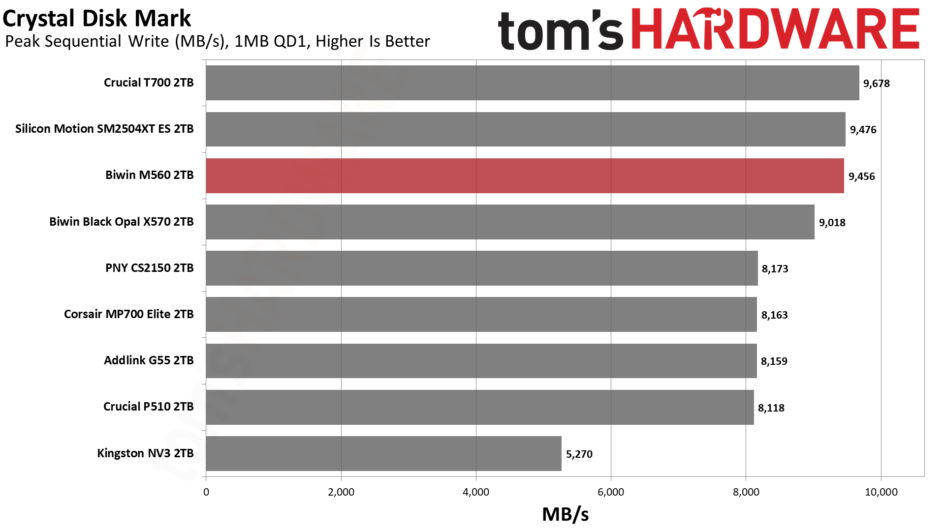
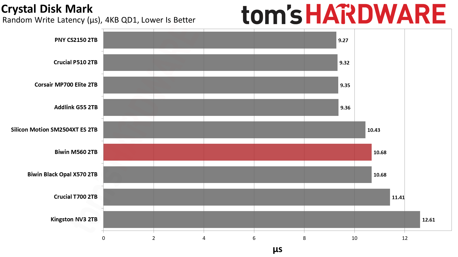
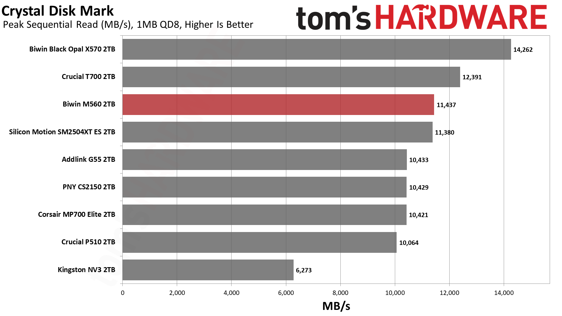
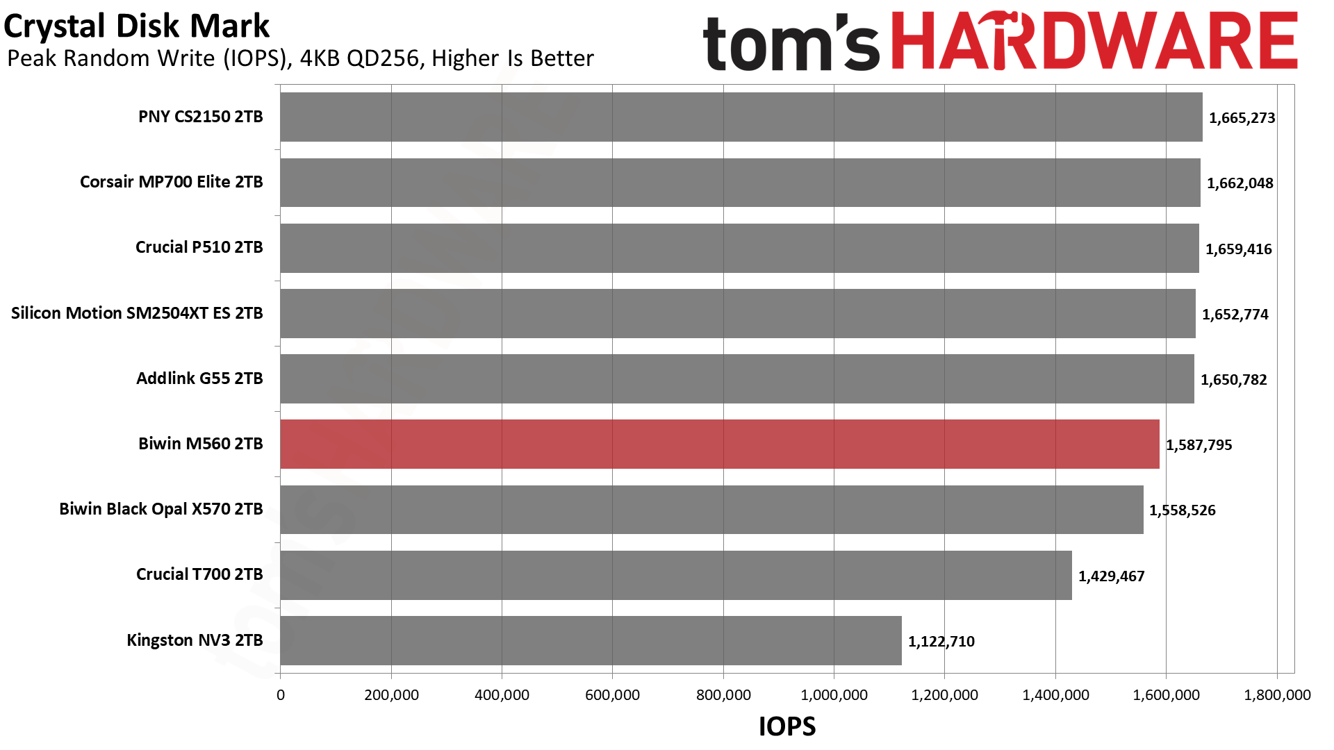
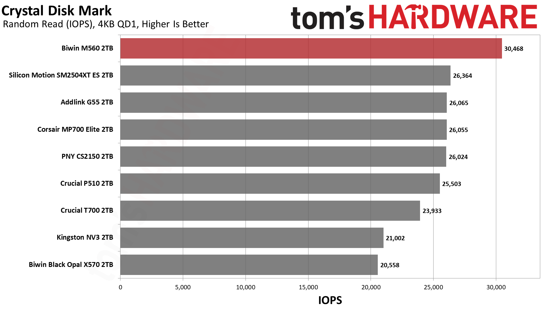
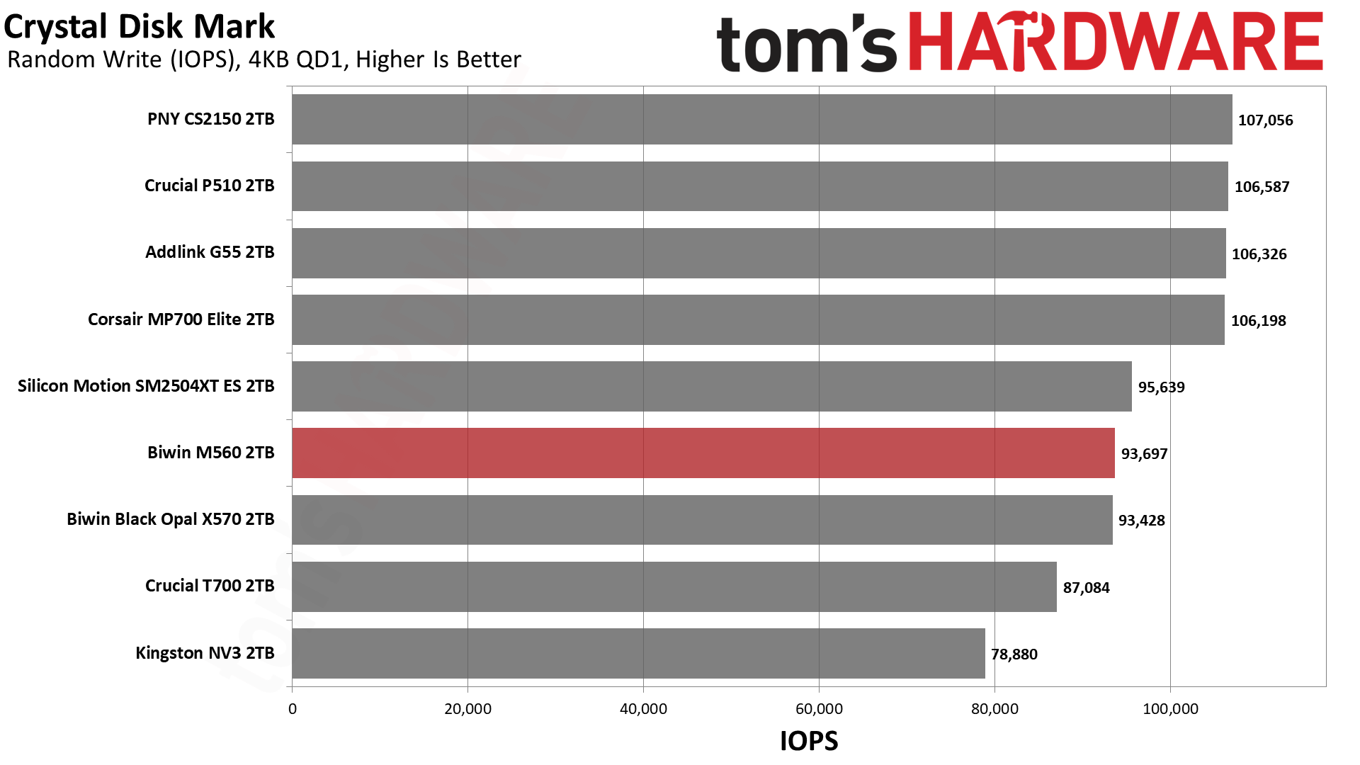
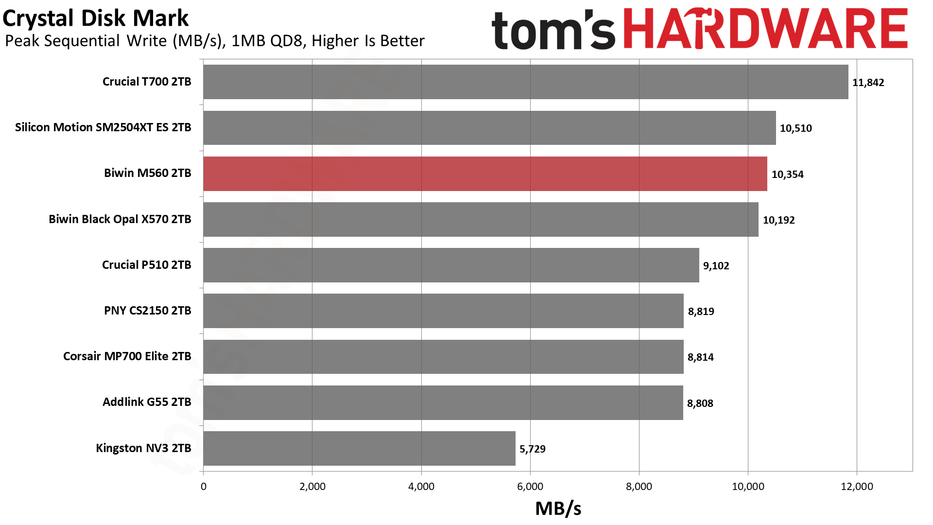
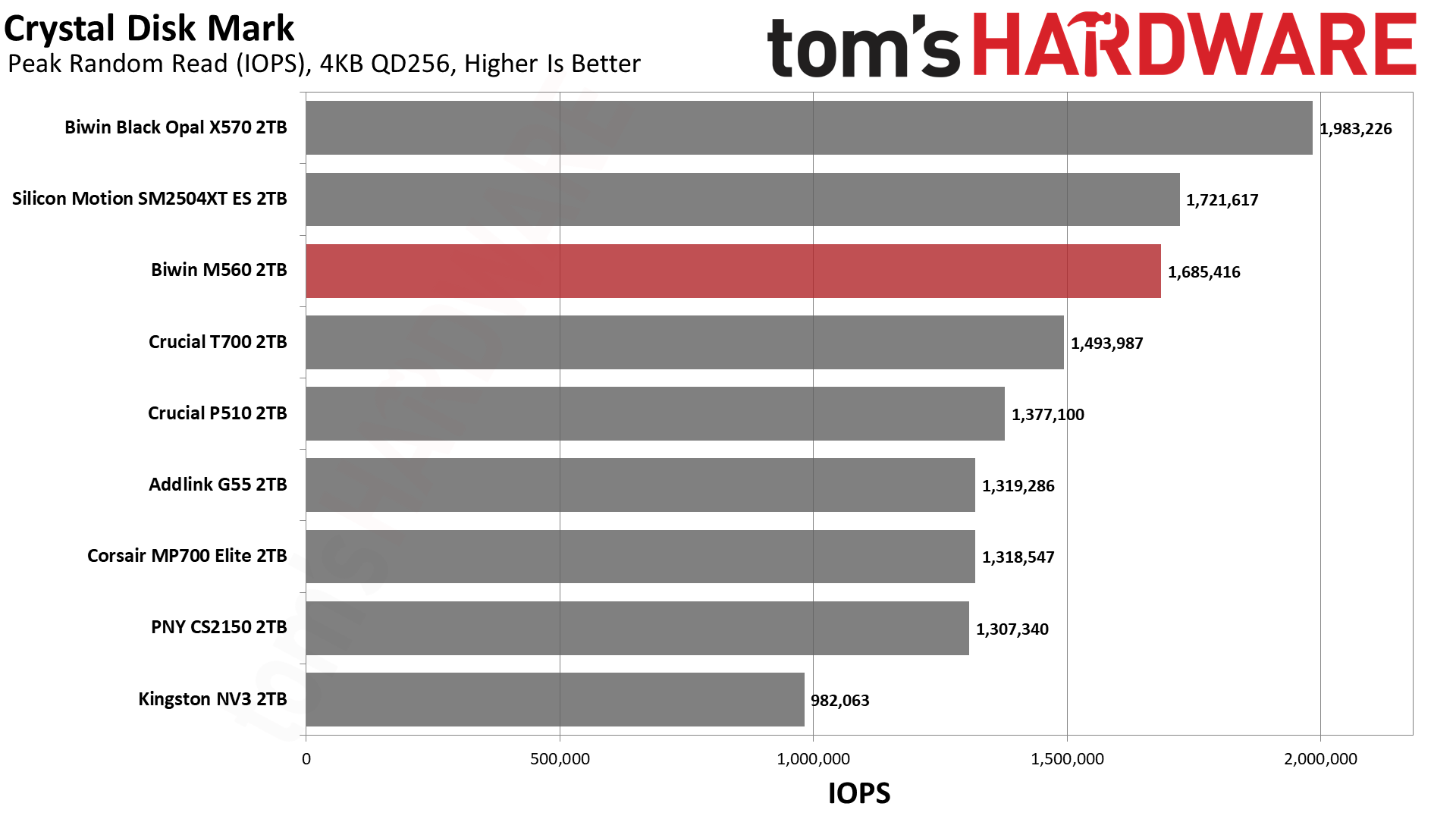
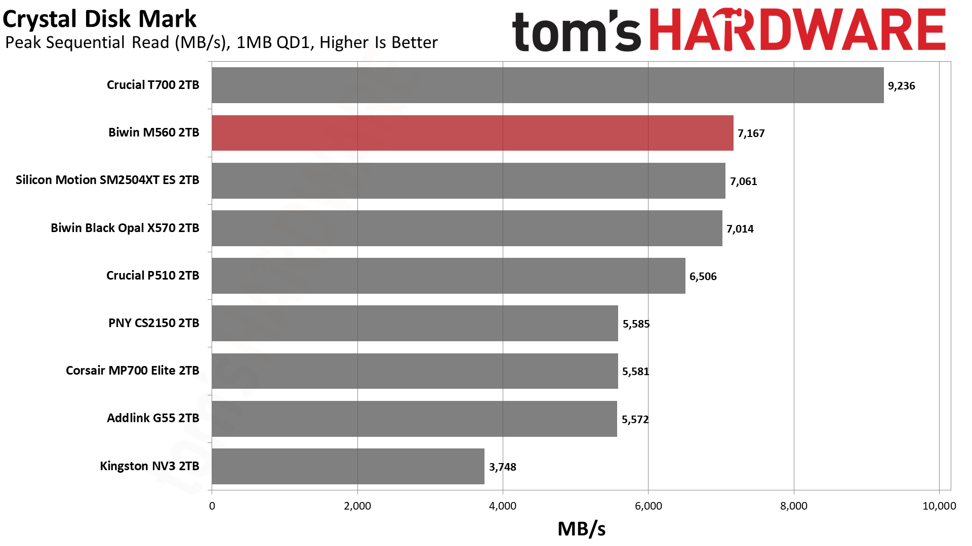
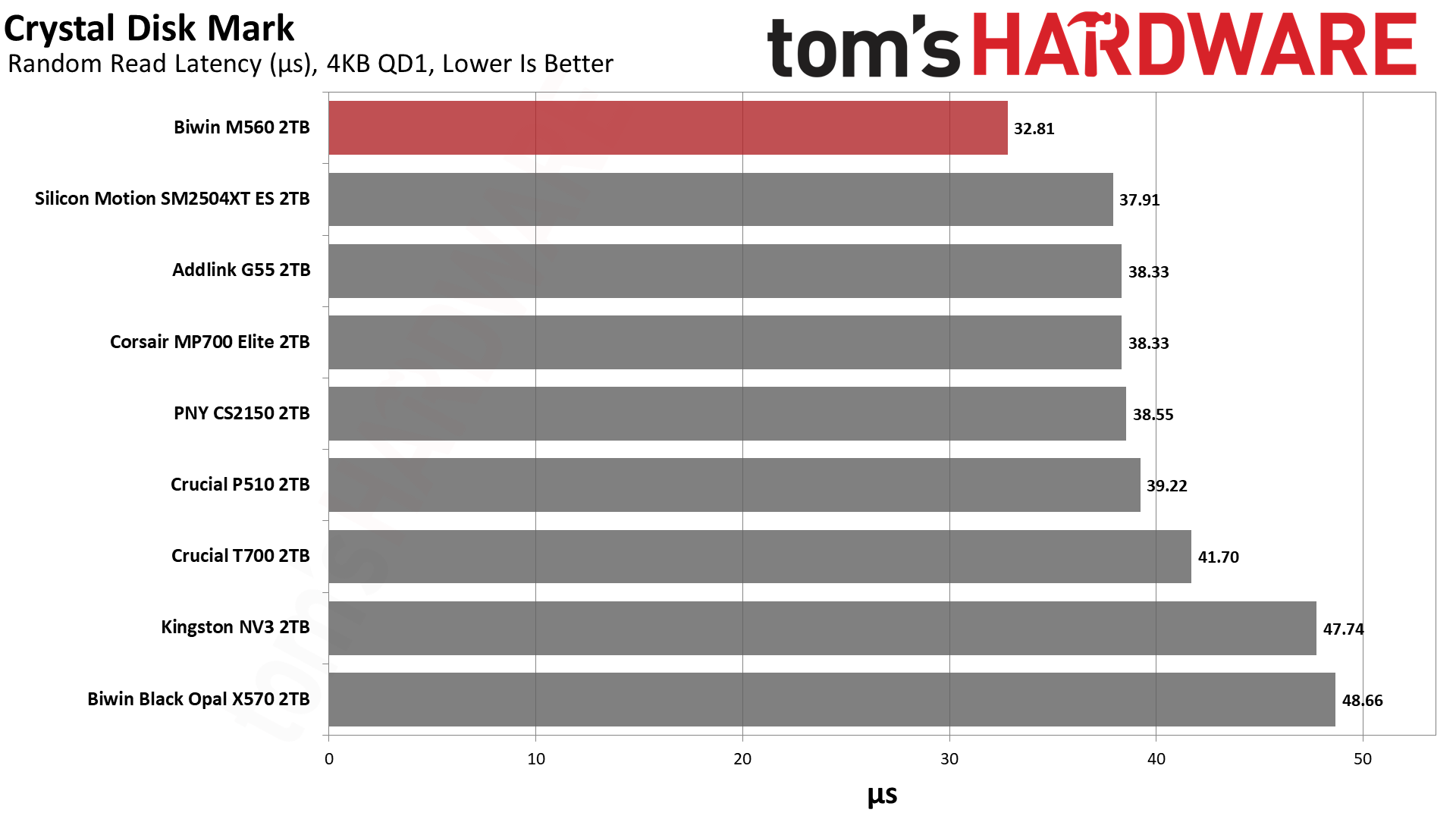
If we turn our attention towards CDM, we see that it dominates with sequential performance against not only the other retail drives in its class but the X570 as well, except at QD8 for reads. This is a powerhouse for what it is. If we look at 4KB performance, we see two different things, with one that weighs more than the other. The first is 4KB QD1 random write latency, which isn’t bad but not up to the level of what we’ve seen with this flash. The maximum IOPS at QD256 also lags. For reads, though, the M560 comes into its own: ahead of the E31T drives at high QD for 4KB random reads but, more importantly, top in QD1 latency against all drives here.
That result, more than any other, should compel you to consider this drive. It’s exceptionally responsive for what matters in daily use. It’s not quite as fast as WD and Sandisk’s drives with Sandisk BiCS8 flash, but it’s very close. Phison’s E31T just doesn’t come close.
Sustained Write Performance and Cache Recovery
Official write specifications are only part of the performance picture. Most SSDs implement a write cache, which is a fast area of pseudo-SLC (single-bit) programmed flash that absorbs incoming data. Sustained write speeds can suffer tremendously once the workload spills outside of the cache and into the "native" TLC (three-bit) or QLC (four-bit) flash. Performance can suffer even more if the drive is forced to fold, the process of migrating data out of the cache in order to free up space for further incoming data.
We use Iometer to hammer the SSD with sequential writes for 15 minutes to measure both the size of the write cache and performance after the cache is saturated. We also monitor cache recovery via multiple idle rounds. This process shows the performance of the drive in various states including the steady state write performance.
Tom's HardwareTom's HardwareTom's Hardware
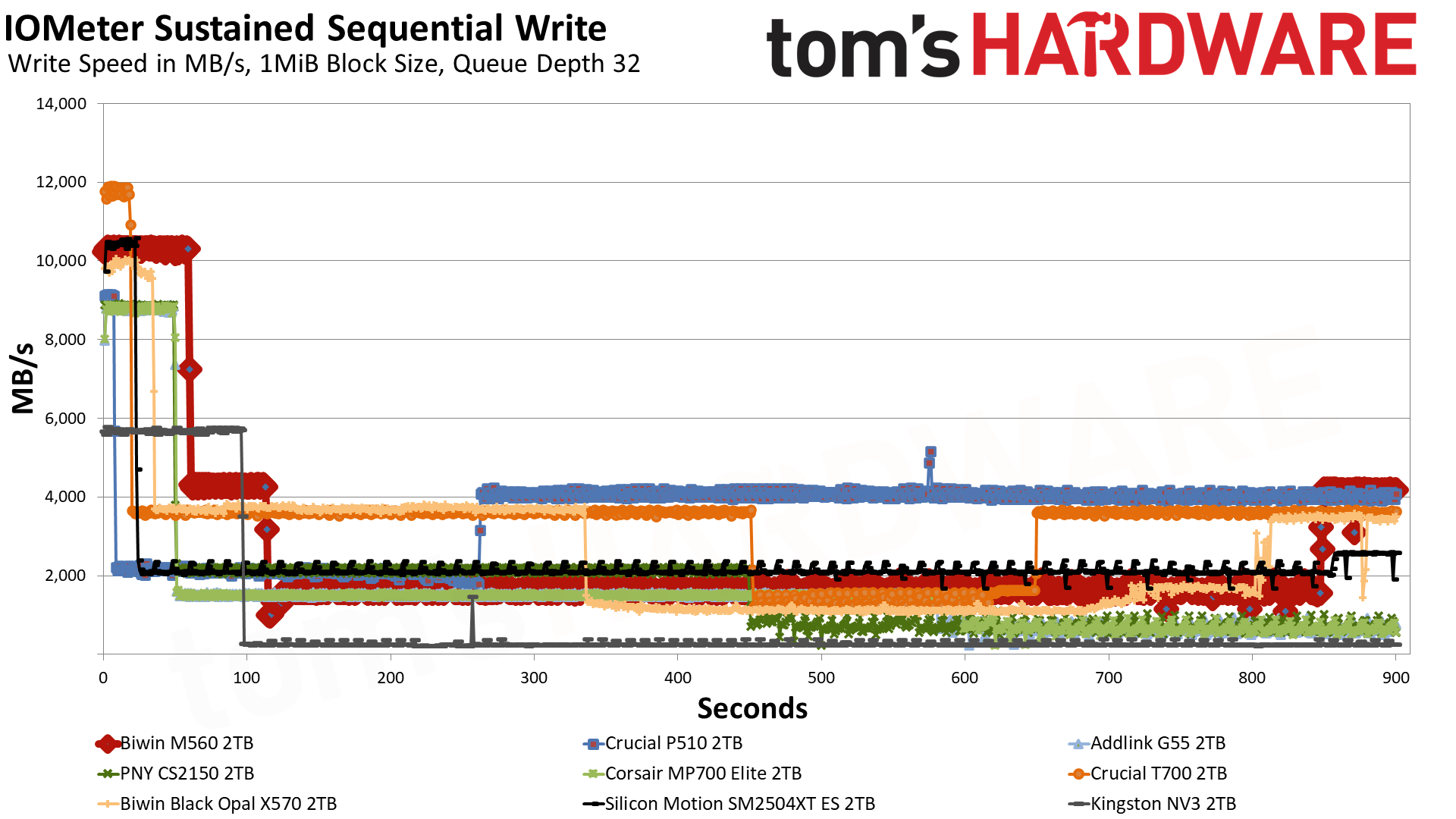
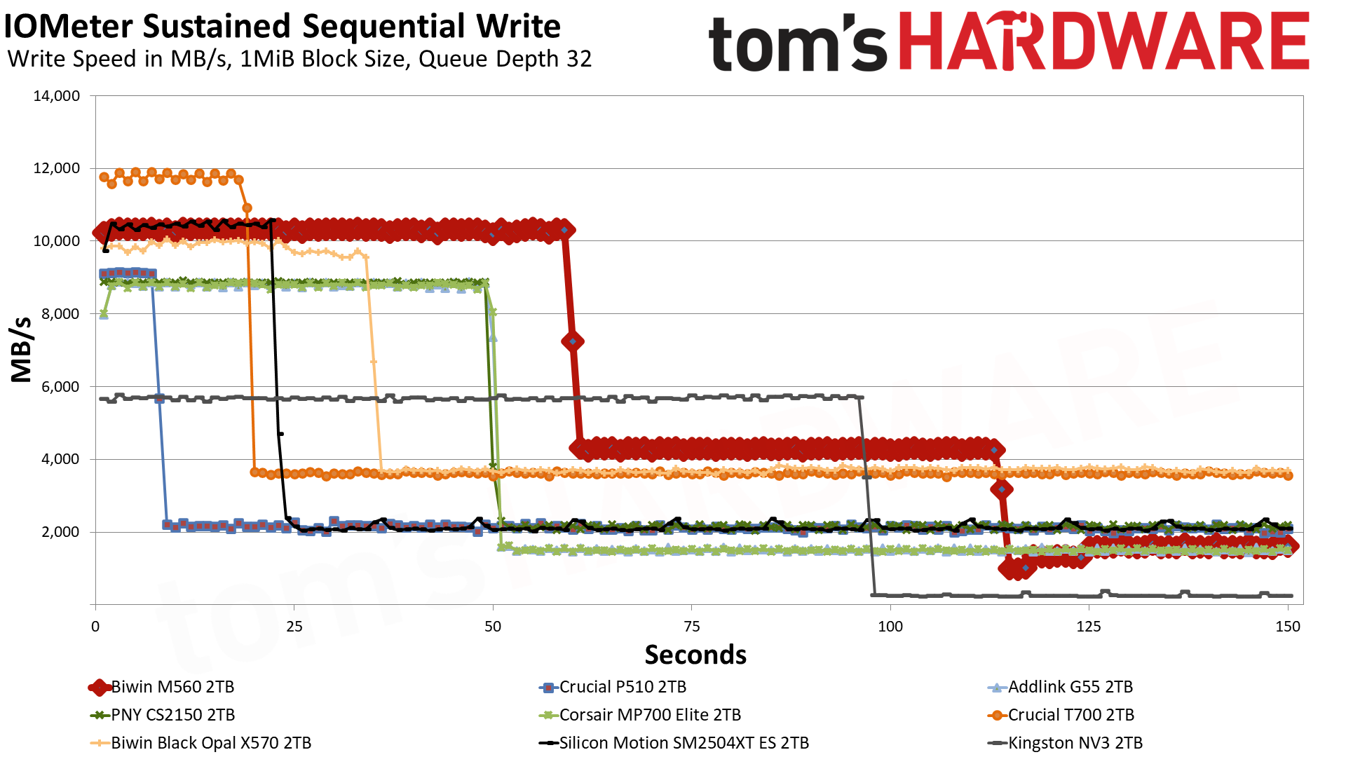
The M560 has three distinct write states: the pSLC cache, direct to TLC flash, and a folding mode where it has to wait for data to be moved over from the pSLC to the TLC. In the first mode, it writes at an average of over 10.3 GB/s for over 59 seconds with a cache of around 611 GB. This is plenty fast for a drive of this type, and the cache is a good size. That figure is from an empty drive, and as with any dynamic cache, it will shrink as the drive fills. It is possible to dedicate more of the TLC flash to this mode, but that has drawbacks. A larger cache usually means the drive will be slower and less consistent with writes when the cache is exhausted.
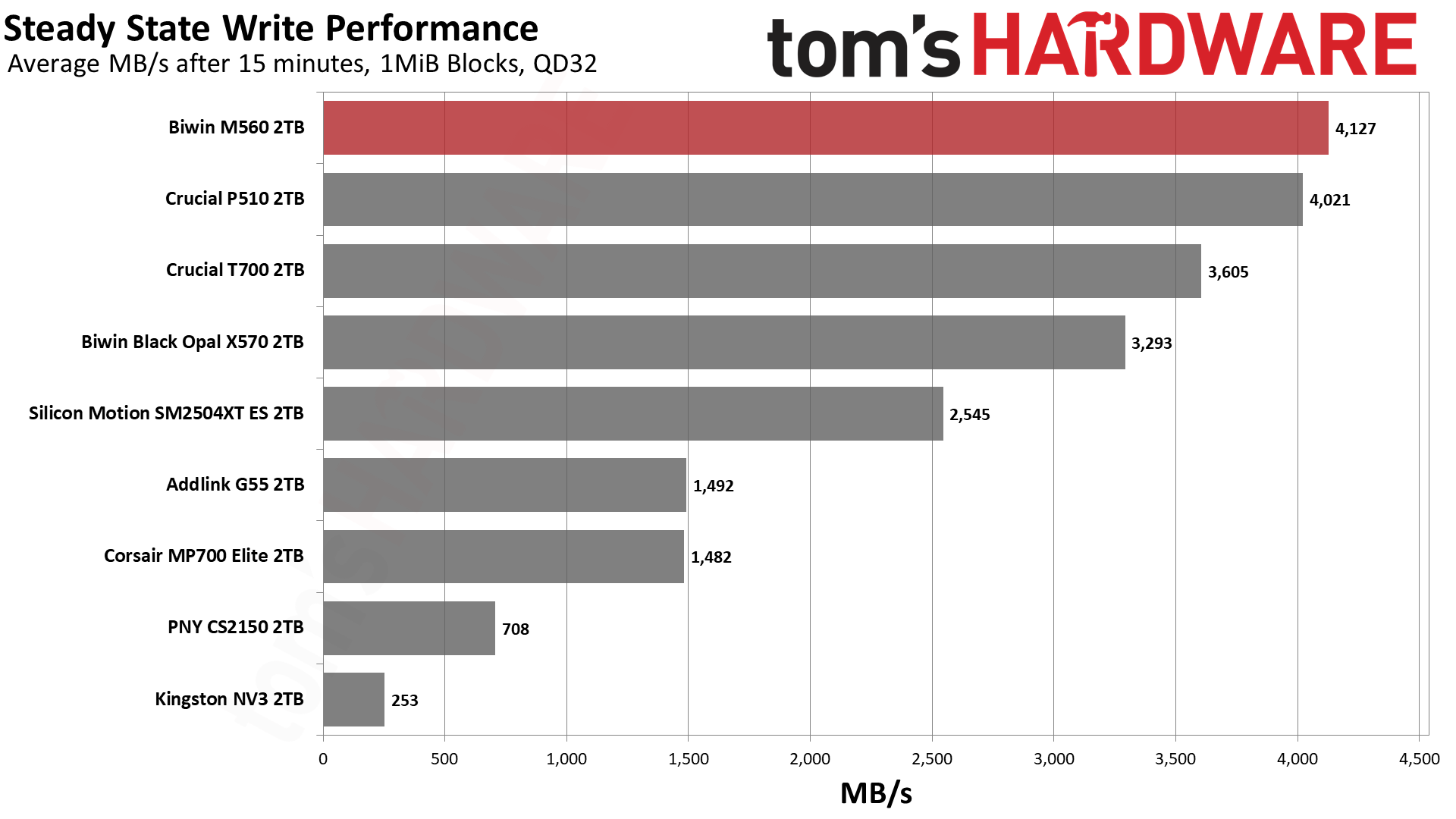
In the middle native write mode, the drive writes at over 4.1 GB/s, which is also what our steady-state result shows: that chart averages the last 30 seconds of the run, and by then the drive had written about 2TB and was back to writing at its native speed. This is in part misleading and in part not. It’s not misleading because, in fact, the flash can maintain this native speed under the right circumstances. It is misleading that you’d end up with this at the end of your writes because the drive will outrun the cache, and there will not be enough space left to handle the incoming writes. This forces the drive to “fold” data from the cache to the native TLC, which interferes with the direct write process, increasing latency and lowering the write speed. The resulting speed is usually less than half the native and, in this case, is somewhere above 1.6 GB/s, which is by no means terrible when some QLC-based drives end up at 10% of that. Note, however, that the ES we tested with the same hardware has a more consistent 2.1 GB/s write speed line, and this is due to it having a much smaller cache.
While the large cache here means that this drive really isn’t ideal for sustained write workloads, the fact it can get over 4 GB/s with its flash is pretty incredible. This would have been above and beyond just about every PCIe 4.0 drive in existence, and with just half the channels. This is a very fast drive and, frankly, feels like a high-end drive if you can get past the fact it “only” hits a bit above 10 GB/s. In practice, for longer writes that still fit in its roughly 600 GB cache, it’s going to feel like one of the fastest drives out there. It’s just that some drives, like the P510, would be more suitable for write workloads where you want a smaller cache. Alternative cache configurations for this same hardware would also be better for that, but we have few to compare at the moment.
Power Consumption and Temperature
We use the Quarch HD Programmable Power Module to gain a deeper understanding of power characteristics. Idle power consumption is an important aspect to consider, especially if you're looking for a laptop upgrade, as even the best ultrabooks can have mediocre stock storage in terms of capacity and performance. Desktops are often more performance-oriented with less support for power-saving features, so we show the worst-case for idle.
Some SSDs can consume watts of power at idle while better-suited ones sip just milliwatts. Average workload power consumption and max consumption are two other aspects of power consumption, but performance-per-watt, or efficiency, is more important. A drive might consume more power during any given workload, but accomplishing a task faster allows the drive to drop into an idle state more quickly, ultimately saving energy.
For temperature recording, we currently poll the drive’s primary composite sensor during testing with a ~22°C ambient. Our testing is rigorous enough to heat the drive to a realistic ceiling temperature, but real-world temperatures will vary due to the environment and workload factors.
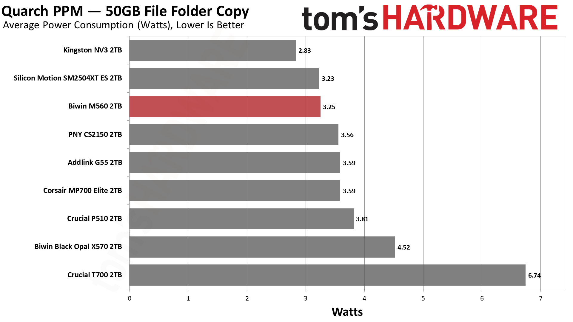
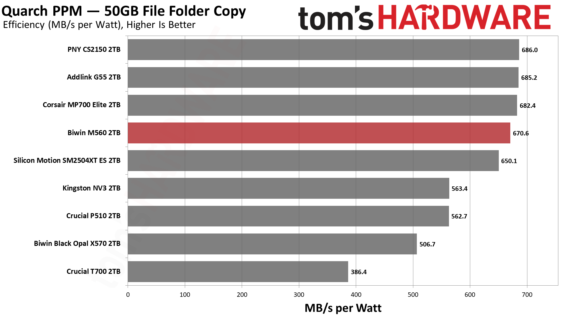
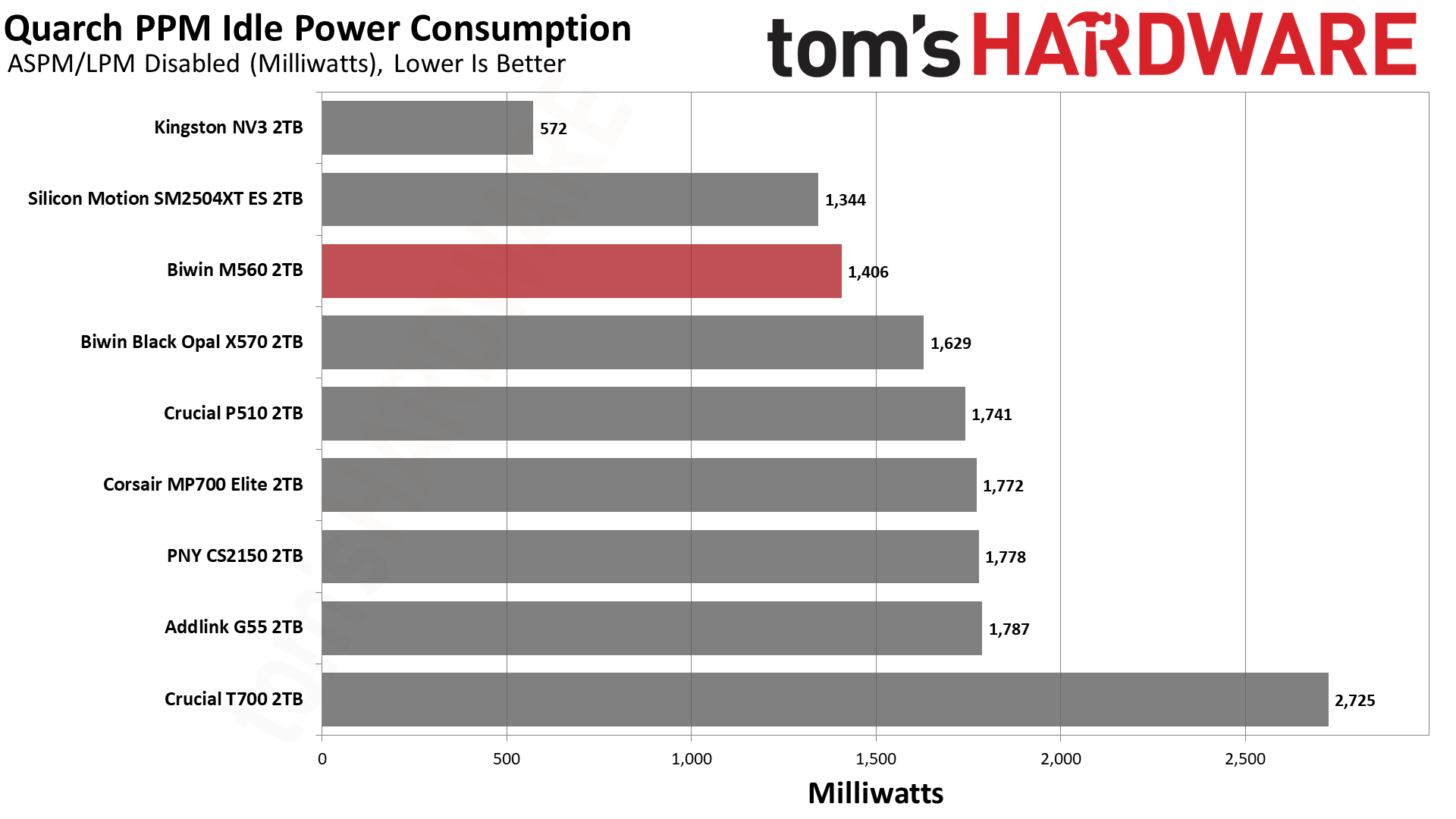
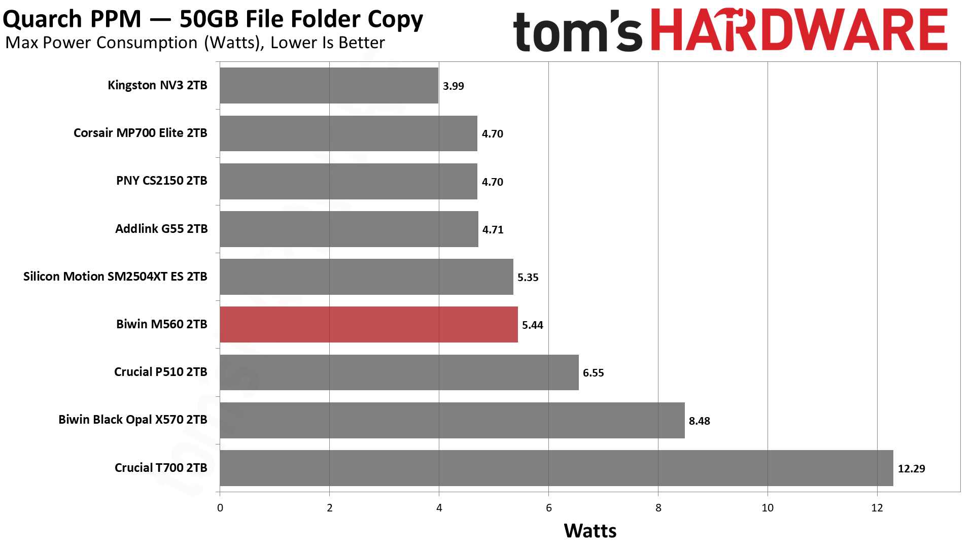
Given what we know from our ES preview, it comes as no surprise that the M560 is efficient. Very efficient. It’s a little shy of the numbers the Phison E31T drives with BiCS8 can put up, but it’s close enough to be negligible. It can pull more watts at peak, but the number is still manageable, and the average power draw is also superior. In fact, the idle power consumption is also relatively good, better than the Phison drives. Ideally, your system will be able to save power, but in the case where you favor responsiveness, the M560 does pull slightly fewer watts. Our take is that, on the whole, this drive delivers pretty excellent power numbers.
The drive ran relatively cool, too. The two sensors hit maximums of 61 and 76 degrees Celsius, respectively. This puts the latter about 10 degrees below throttling, which is closer than we like but is also plenty respectable for a fast, PCIe 5.0 SSD without a heatsink. We test during heavy writing, and the drive has a chonky cache, so we’d expect normal use to run somewhat cooler on average. Sensors aren’t always accurate, and we suspect the hotter one is showing the controller’s temperature, in which case this would probably be okay in most laptops. Would a heatsink help? Sure, but it shouldn’t be a requirement with how few watts this drive draws on average.
We use an Alder Lake platform with most background applications such as indexing, Windows updates, and antivirus disabled in the OS to reduce run-to-run variability. Each SSD is prefilled to 50% capacity and tested as a secondary device. Unless noted, we use active cooling for all SSDs.
Biwin M560 Bottom Line
The Biwin M560 is one of the best all-around drives we’ve ever tested and, for its intended role, is probably the best retail option available. That “role” would be acting as a fast, capable, and efficient all-around boot or primary drive that also has to do other things, like handle gaming and work. Its 1TB and 2TB SKU range underlines this; it’s not a budget drive, and it’s not a storage drive. Not everybody needs or wants a monster 14+ GB/s drive with DRAM, but you might still want to take advantage of newer hardware. This hardware is faster, yes, particularly with insanely low 4KB read latency, but is also very power-efficient. It’s a good option even for PCIe 4.0 laptops, with the future-proofing an added bonus.
(Image credit: Tom's Hardware)
We have few complaints about the drive as a whole, except maybe that a 4TB option would have been nice, but we can live without it. From the performance side, things look very good, but we would be remiss if we didn’t point out that Biwin went with a large cache here. That has its plusses and its minuses. For the expected role, it was probably the right call. The drive also faltered a bit in DiskBench, but this only underlines our point about where it belongs: with lower performance there, the drive makes less sense as a second or third drive. Make no mistake, the M560 is quite capable of being your main drive as a very acceptable alternative to a more expensive Black SN8100 or equivalent.
As it is, we can highly recommend this drive. It’s one of the most responsive drives we’ve ever used and really feels “next gen,” whatever that might mean for an SSD. You should still go with a 4TB PCIe 4.0 DRAM-less option, like the A93 or NM790, if you want fast storage. Or a 2TB Black SN8100 if you want the very fastest main drive. Or something cheap for a secondary or games drive. If you want DRAM and can handle the heat, there are options there, too.
If, on the other hand, you want a dynamite drive that delivers a solid experience, something that won’t hold your desktop or laptop back, then the Biwin M560 would be at the top of our list.
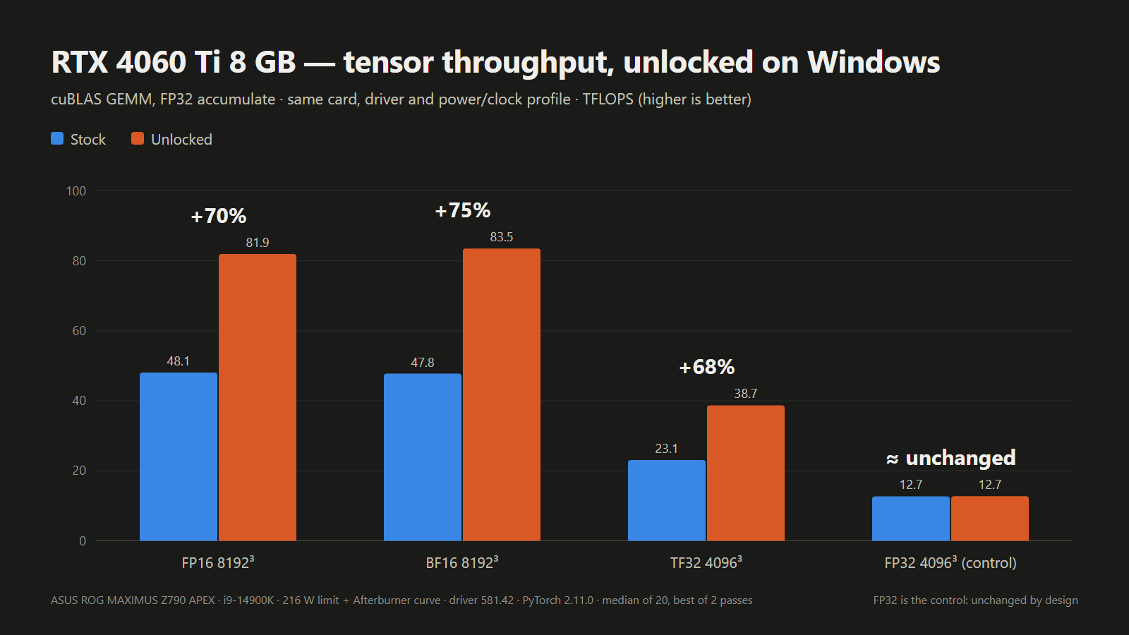
A new open-source UEFI tool boots from USB and unlocks significant extra tensor performance on RTX 20, 30, and 40-series desktop and laptop GPUs, making the half-speed AI throttle hack a whole lot easier to try on Windows. No VBIOS flash or patched driver needed: the tool runs from a FAT32 stick before the Nvidia driver loads at every boot, and then voila, the developer’s own laptop RTX 4060 hit 65% higher FP16 math.
The “UEFI pre-driver NVIDIA GPU unlocker,” or nv-uefi-unlocker project, removes Nvidia’s tensor limiter using the community V67 payload with read-back verification. This tricks Nvidia’s signed Booter firmware into opening the write lock on two speed-selector registers, allowing the tensor units to run at full rate. The unlock can now run entirely from a bootable USB drive, on Windows as well as Linux, whereas previously it worked primarily through manually installed Linux modules, with Windows support only experimental. The read-back verification part makes things safer, which was a concern with the experimental builds.
The release ships only scripts and self-built binaries, without any Nvidia firmware in the download. Instead, one of the scripts grabs Nvidia’s public 610.43.03 driver packages, verifies them, then rebuilds the firmware files locally. The project credits Zagitta’s gpu-unlock as its porting source and builds on several other community projects, including the RTX 40 fork gpu-unlock-ada and an earlier Windows EFI tool. Having one tool for the many GeForce owners on Windows should significantly open up the hack to a wider audience. Previously, it was scarier-looking, and project progression is rapid these days with AI tools.
The steps right now involve downloading the release, running that script, and then copying the rebuilt files and a BOOTX64.EFI for booting to a FAT32-formatted USB stick. The unlocker can then be run from a one-time boot menu by using the spacebar within 30 seconds for confirmation. Once complete, things are handed off to the respective OS loader.
The unlocker runs in a firmware stage before the OS loads Nvidia’s GPU driver, which means there’s no need to flash the card’s video BIOS or to modify the driver; as the FAQ puts it, the unlock doesn’t “persist through power loss.” The trade-off is running it again on every boot. The system must be booted in UEFI mode with Secure Boot either off or set to trust a self-signed EFI. For a game’s anti-cheat that requires Secure Boot, the tool “CANNOT bypass this requirement,” a developer team member relayed on Reddit. RTX 20 owners have to run a bundled script once to switch the Windows Nvidia driver into GSP firmware mode, before restarting.
Laptop GPUs were already supported by earlier projects, but here one of the developer’s own test cards is a laptop GPU, and laptop results are logged card by card. For laptops, the discrete Nvidia GPU must be powered at entry, which means dGPU-only, or MUX, mode is recommended. On Linux distributions such as Ubuntu, runtime power management can power down the GPU when idle and silently erase the unlock. The English FAQ covers workarounds for this, with instructions and guidelines for other situations.
Compatibility otherwise includes RTX 20-series support listed as “fully compatible; some models have known issues,” while RTX 30-series cards are “fully compatible,” and the tool is “fully compatible on laptops and desktops” using RTX 40-series cards. The GTX 16 is “theoretically compatible” with verification pending, but other cards, including pre-Turing, the GA100, and RTX 50-series cards, are unsupported. The project routes support by chip family, so a card being covered doesn’t mean that specific card has been tested. Cards verified by the tool’s own Windows results are listed in the table below.
Which GeForce cards nv-uefi-unlocker has run on
Generation
Confirmed working on Windows
Known problems or untested
RTX 20 (Turing)
RTX 2070, RTX 2060 Super
RTX 2080, 2080 Ti and 2080 Super fail at boot or handoff; GTX 16 untested; needs GSP firmware mode and a restart first
RTX 3050 untested; persistence on Thunderbolt eGPUs not guaranteed
RTX 40 (Ada Lovelace)
RTX 4090, 4080, 4070 Ti Super, 4070 Super, 4070, 4060 Ti 8GB and 16GB, 4060 Laptop, 4050 Laptop
RTX 4070 Laptop untested
RTX 50 (Blackwell)
None
Not supported
Results compare each card before and after the unlock on the same test, but the tests differ from row to row, so they shouldn’t be compared across cards.
Reported Windows results with nv-uefi-unlocker
Card
Test (FP32 accumulate)
Stock (TFLOPS)
Unlocked (TFLOPS)
Gain
Who measured
RTX 2070
FP16 matrix multiply
36
60–63
+67–75%
Developer
RTX 3060 12GB
FP16 matrix multiply, 4096
25.37
45.79
1.80x
Owner report
RTX 3070 Laptop
FP16 matrix multiply, 8192
35.43
56.04
1.58x
Owner report
RTX 4060 Laptop
FP16 matrix multiply
29.89
49.33
1.65x
Developer
RTX 4080
BF16 matrix multiply, 4096
100.37
192.18
1.91x
Owner report
RTX 4090
FP16 matrix multiply, 4096
118.42
171.52
1.45x (power-limited)
Owner report
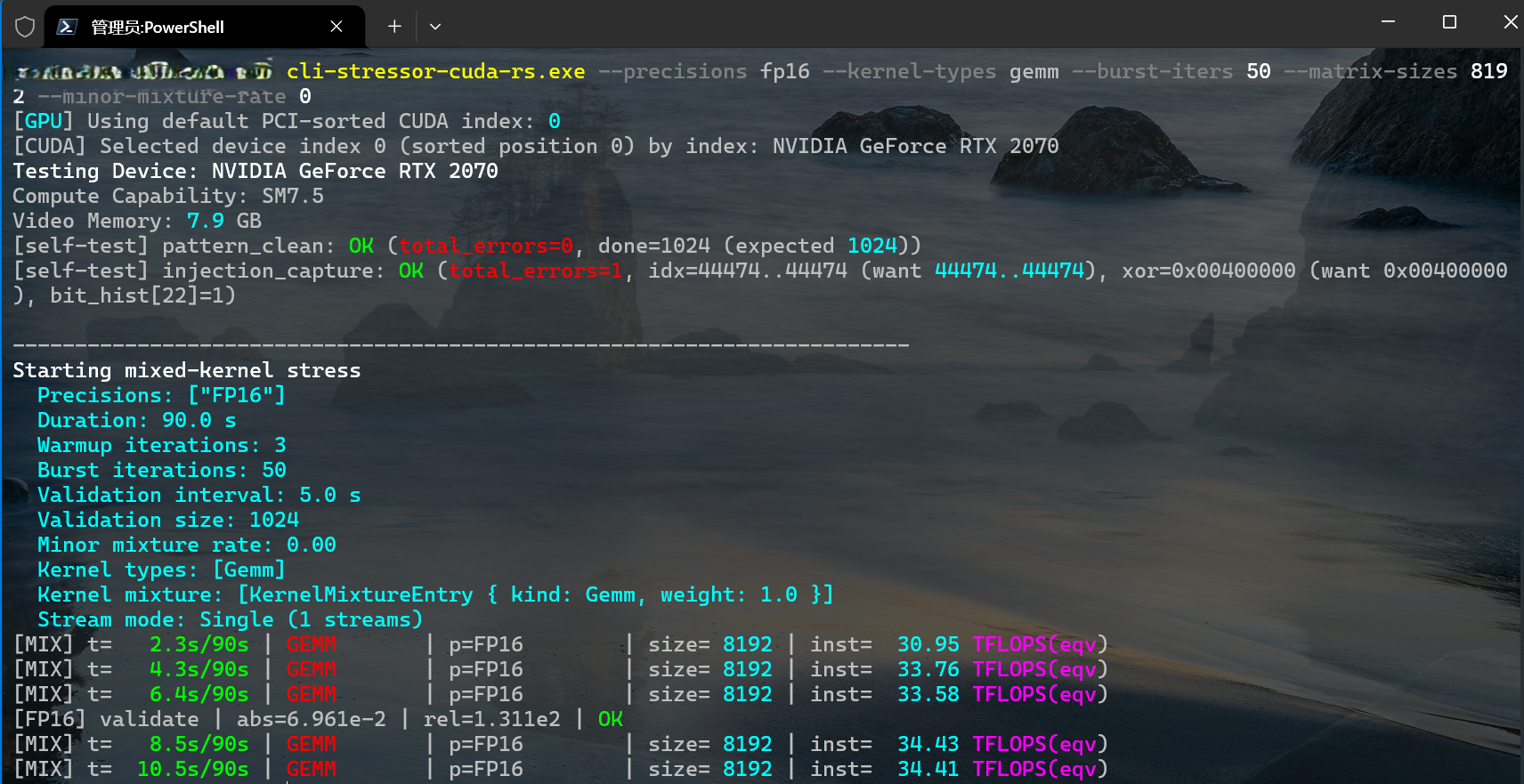
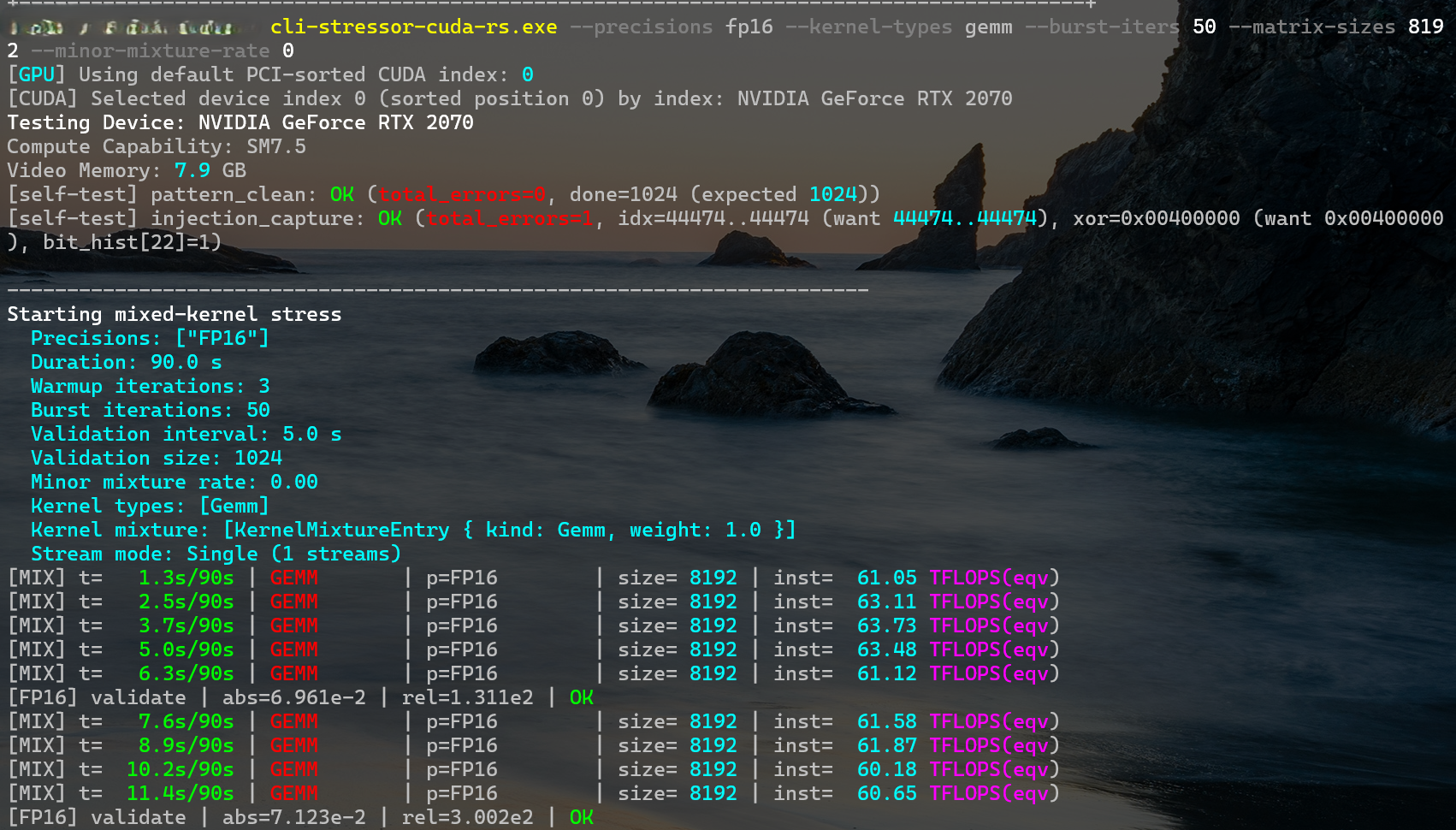
The developer’s own desktop RTX 2070 went from about 34 TFLOPS in FP16 matrix multiply at 8192 to around 62 TFLOPS in the screenshots below.
physicsdolphin/GitHubphysicsdolphin/GitHub
Some caveats still exist, and Zagitta, whose gpu-unlock kicked off the GeForce unlocks, now says in its FAQ that “I don’t run windows and don’t plan to maintain it,” pointing Windows users to a separate port and warning to be careful with unofficial Windows installers. Results from the unlock are also contingent on power and thermal limits. The new project says it can be combined with the nvoc power-limit unlock, but warns this “can exceed factory power and thermal envelopes.” A per-card ROM hash check, which the project’s own safety rules require, isn’t built yet, and the unlock’s persistence on Thunderbolt eGPUs “is not guaranteed.”
Other cards, including the RTX 2080 and the RTX 2080 Ti, are under review. No dates are promised. The pro-card tensor feature can now be unlocked for many, though, and as simply as using a USB boot drive, which will get even easier with a boot-from-disk toggle the team says is in the works. RTX 50-series owners have to wait, for now, as the team is still trying to crack those cards, which have “a lot more security” than it anticipated.
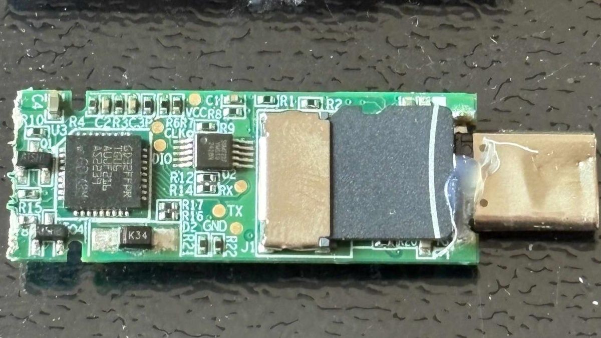
Security researcher Xusheng Li found that a Lenovo ThinkPlus FU100 fingerprint USB stick, sold as an AES-256-encrypted device for data security, ended up being just a plain SD card internally,HackingPassion reports. The fingerprint reader only enabled the USB connection, and nothing on the card was actually encrypted. An AI-assisted follow-up last week discovered what Li calls backdoor accounts on another maker’s drive, as well as hardcoded keys in other supposedly secure USB storage products.
The FU100 is “just an SD card in a fancy case,” Li said in a March conference talk. It is, as a result, trivial for anyone with physical access to get to the drive’s data. One of his takeaways: “‘Hardware security’ can be pure marketing.” This isn’t the first timedrive makers’ own encryption has failed, and it won’t be the last.
The original ThinkPlus FU100 analysis happened last year, with an interim fix using epoxy over the card. A later fix by Lenovo, put out early this year for the FU100, FU200 and TU800 drives, as well as the TSD303 SSD, requires owners to call a China service line, then either send devices back for replacement or get an on-site firmware upgrade. Lenovo advises backing up data first and strongly recommends wiping the drive before sending it in, which is quite an inconvenience. Lenovo rated the advisory’s severity as high, and one of its three CVEs covers the configuration software, which could let a local, logged-in user bypass device authentication and enroll an untrusted fingerprint.
The same research also turned up a different flaw in Lenovo’s TSD303 external SSD. Its data actually was encrypted, but the drive sent the correct password back over USB in plain text for the software to compare, making it easy to capture. The first fix came three months after the initial report, using block cipher encryption with a key derived from a timestamp-like value. Lenovo’s software could derive that key, and the first software fix is vulnerable if taken apart, making it not useful for protecting data if a device is stolen. A later fix, late last year, has the drive check the typed password itself, so the correct one never leaves the drive.
The same software development kit used for the drive covered nine other devices from multiple vendors, most of which could also reveal passwords to a savvy actor. In addition, two left data unencrypted on a microSD card. The full list of vendors was blacked out on Li’s slides.
AI agent use fordriving reverse-engineering tools continues to increase. AI has also beenexposing more security flaws recently. Li used OpenAI’s Codex, an AI programming-centric tool, with his employer’s reverse-engineering tool against other vendors’ protection schemes. Netac’s tool took about seven minutes to break, as Codex found a fixed key built into the program, along with the user’s password written to diagnostic logs.
Copy protection differs from direct access, as the intent is to allow the recipient to view files, just not make copies of them. KakaSoft’s USB Copy Protection has an internal password the program builds itself, which Codex rebuilt to decrypt a test file without the user’s password in around 26 minutes. Nexcopy’s Copy Secure took about 10 minutes, with its key unlocked by a certificate built into the viewer app. Separately, SecZure’s YutianDun has two hidden “backdoor” accounts with simple passwords, discovered with time-travel debugging, stepping through a timeline trace. However, Li’s comments suggest that malicious intent cannot be assumed.
Li gave no warning to KakaSoft, Nexcopy, or SecZure, arguing that a drive already in an attacker’s hands can’t easily be recalled or updated. He said that “client-side validation is never secure” and you should always verify security claims on your own. Netac had no patch as of Li’s March talk. An example of things done right would bean open-source USB stick that does encryption properly, even though it is built on a microSD card, deriving its key from the user’s password, so reading the card alone gets an attacker nothing.
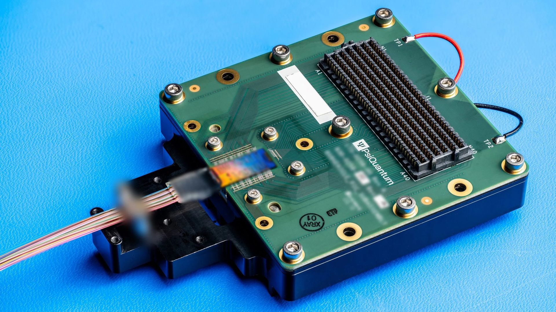
PsiQuantum, a quantum computing company, announced in a release earlier this week that it has turned its low-loss silicon photonics into an optical switch for use in AI data centers. Every optical switch typically comes with loss of light: the more light a switch receives, the less reaches the other side, with the amount of light lost measured in decibels. Typical data center optics can tolerate half the light (3 dB) being lost. PsiQuantum's switch debuted with a demo that typically loses only 1.2 dB of signal, or about a quarter of the light in lab tests, and the all-optical switch can achieve it without an amplifier. The prototype is, however, comparatively small, with eight inputs and outputs (8x8) against competitors’ 32 to 300, but the company says larger devices are in development.
The optical circuit switch (OCS) passes light straight through, from fiber to fiber, without converting it to or from electrical signals. Regular data center switches make that conversion at every hop, which takes power and adds latency. An OCS, instead, uses a fixed light path that it maintains until a change is ordered. Its main penalty comes down to how much light is lost when passing through the switch. PsiQuantum’s switch, which uses circuits etched on a silicon chip with no moving parts, unlike Google’s and Lumentum’s tiny mirrors, or microelectromechanical systems (MEMS), would be used alongside regular packet switches.
Skipping those conversions matters more as AI clusters grow, because moving data between GPUs is quickly becoming a bottleneck. Optics are a high-bandwidth improvement over copper, which has limitations in reach, although a shortage of lasers is a problem for the alternative. Improving communication bandwidth and distance is the goal, so that different racks of GPUs can talk at speed and act as one.
Switches similar to PsiQuantum’s made by Salience Labs and iPronics use built-in amplification and, at least in the former case, are also rated at under 2 dB, or under 37% of the light lost. Google’s mirror-based switch, Palomar, can also typically stay under 2 dB and has 136 ports. Salience’s switch sits at 32 and Lumentum’s at 300, which leaves the eight-port prototype a ways behind on how many fibers it can handle.
Optical circuit switches by loss and size
Switch
Ports (in × out)
Insertion loss, and what the figure is
Reconfiguration
How it switches
PsiQuantum 8×8 demo
8×8
1.2 dB (about 24% of the light lost), typical in the company’s lab tests
Under 3 ms
Silicon photonics chip, no amplification, no moving parts
Google Palomar
136×136
Typically under 2 dB (under 37% lost) across all port pairings; 2 dB worst case
Milliseconds
MEMS mirrors (moving parts)
Lumentum R300
300×300
Close to 1.5 dB (about 29% lost), typical at start of life, Lumentum’s switching GM told Gazettabyte
Not stated
MEMS mirrors (moving parts)
Salience Labs OC-32M
32×32
Under 2 dB (under 37% lost) port to port, a ceiling, after built-in amplification
Under 300 µs
Silicon photonics chip with amplification
iPronics ONE-32
32 (layout not stated)
Not published
Under 300 µs
Silicon photonics chip with optical amplifiers
PsiQuantum's switch is an 8x8, meaning eight in and eight out, and “every input can reach every output.” It’s also “strictly non-blocking,” so a new connection never disturbs ones already in place. In the lab, it measured a typical 1.2 dB insertion loss, 40 dB of crosstalk (about 0.01% of the light leaking to other ports), and under 3 ms of reconfiguration time, all of which exceed “initial targets set for these devices.” The loss figure is measured fiber to fiber, which includes getting light onto and off the chip but not connector losses, PsiQuantum told Tom’s Hardware Premium.
The platform loses very little light at each component, which matters because a quantum computer can tolerate only so much lost light. PsiQuantum’s 2025 Nature paper reports silicon nitride waveguides losing as little as 0.5 dB per meter (about 11% of the light per meter), splitters 0.5 millidecibels, and crossings 1.2 millidecibels, the last two a few hundredths of a percent of the light or less each.
The company also says chip-to-fiber coupling has reached about 60 millidecibels, roughly 1.4% of the light lost, in its best published lab results, although without a full fiber array attached. Those figures set a best case, not a worst case, for a 64-port switch, since light crosses more components as ports are added and the losses add up.
How much loss is acceptable varies with the optics at the end of each link. Coherent, an optics maker, says that using an OCS can add “up to 3 dB additional insertion loss,” but its transceivers are able to work with that. Lumentum told Gazettabytethat 3 dB is good enough to work with off-the-shelf FR4, DR4, and DR8 optical modules using the switch; those are the standard plug-in options used to link GPU servers and switches, at distances of 500 meters to 2 kilometers. PsiQuantum’s 8x8 is built for the O-band, the wavelength range those modules use. PsiQuantum told Semafor that, to be workable, its switch needed insertion loss under 2 to 3 dB.
The 8x8 prototype was designed for conventional data center traffic and comes in well below the 3 dB loss target in a request from Nvidia for proposals, the company says. The port count marks it as a demonstration vehicle, but PsiQuantum has a 64x64 version taped out with a 72x72 underway and is “actively developing larger devices.” With crossings that lose so little light, the scale-up might hold. PsiQuantum declined to share details on future products, though it says the loss, which may be slightly higher, will stay very low.
Speed remains less important than insertion loss for how OCSes are currently used. Google, which has the most deployments, numbering in the “tens of thousands,” uses its switches to resize TPU pods or to route around failed chips, a job its “millisecond-scale” MEMS switches handle. PsiQuantum’s under 3 ms is within that class, but Salience and iPronics claim less than 300 microseconds for their amplified chip switches, which iPronics highlights for mid-workload network rewiring to hide the switch time while chips compute.
There is quite a lot of room for speed to improve, and PsiQuantum already has a material for that, used in an existing 64-port switch for its quantum systems, which need to switch light at gigahertz rates. The material, barium titanate (BTO), changes how it bends light when a voltage is applied, and the company chose it over lithium niobate, a more common selection, because BTO had the strongest effect it could find. This keeps switching elements short and losses low at speeds roughly a million times faster than the demo. BTO is “not required for the demonstration vehicle or initial products,” which use a thermally switched silicon nitride platform, but it is “an additional path to faster, more advanced future products.”
An argument for starting now is that building thousands of such switches for conventional applications would reduce the risk for the packaging, assembly, and supply chain of parts PsiQuantum builds for quantum computing. AI and quantum computing are “complementary technologies,” it says, and this is the chance to put its technology into action. When PsiQuantum hired Rob Soderbery as an executive vice president in July, it said he would advance its silicon photonics platform, “accelerating its application across AI networking and other next-generation computing infrastructure,” hinting at the roadmap. The company’s CHIPS award was finalized in September for “high-performance optical switches,” among other components.
Co-founder Pete Shadbolt praised Google’s alternative MEMS switch but would prefer to have similar-quality switching on a monolithic chip that needs no moving parts. Nvidia has a stake through its venture arm, NVentures, and collaborates with PsiQuantum on “GPU-QPU integration,” that is, graphics and quantum processing units, as well as silicon photonics. Nvidia also joined rival iPronics’ $125 million round in September to develop its second-generation optical switch.
Right now, inside Google, OCSes rewire AI clusters, and research firm Cignal AI expects most deployments to stay there through the end of the decade; outside of Google, OCS is still at “proof-of-concept and early trial.” The firm raised its market estimates earlier this year, though, roughly threefold for 2026 and by more than 40% for 2029. An opening exists for PsiQuantum in GPU networks, which ties into Nvidia’s interest, though adoption there is expected to be limited until then. The company says samples and testing kits have already gone to several computing companies, including GPU vendors and hyperscalers.
PsiQuantum should have commercial products “announced in the coming months,” along with updates on larger devices, while competitor Salience has already demonstrated 64 ports at this year’s European Conference on Optical Communication. Salience’s roadmap already has 128- and 256-port products. Scaling is always an issue, but if PsiQuantum’s figures, which haven’t been independently verified, hold up at 64 ports without amplifiers, then larger monolithic OCSes are on the way.
Anthropic spent less than a third of its $8.9 billion first-half compute bill on serving customers, with most of the rest going into training, research, and running Claude internally, its S-1 filing shows. It has meanwhile signed up for hundreds of billions of dollars more in TPU and GPU capacity. By our math, it has meanwhile signed up for roughly $800 billion more in TPU and GPU capacity, and revenue per compute dollar jumped from $0.40 in Q1 2025 to $2.08 in Q2 2026, which the company links to capacity purchased 12–18 months ahead.
Anthropic’s IPO is likely to beat that of rival OpenAI, which filed confidentially before CEO Sam Altman said its own won’t come this year, amid widespread doubts about an AI bubble. Whether AI labs can cover what it costs to serve their models is an open question.
Anthropic appears to do so easily: it spent $2.4 billion serving customers in the first half of the year, versus $16.3 billion in revenue. Paying for what it has on order is more difficult. Its five compute deals with the biggest stated amounts would cost an estimated $103 billion a year on average once delivered, more than twice its revenue at Q2’s pace of about $46 billion a year. The company also warns that margins may compress as new hardware lands ahead of the revenue it will support.
The company has three main costs: the cost of revenue, which is the inference cost of running Claude for paying customers; R&D, which is mostly compute for training and research into new models plus any internal use; and sales and marketing, which covers the cut taken by channel partners and cloud platform resellers.
Comparing the first half of last year to this year’s, cost of revenue is up about 2.3x, but with revenue up 14x, that means Anthropic keeps an estimated 85 cents for every dollar after serving costs, up from just 12 cents. R&D is up about 5 times, with 66% or more of the compute going to it, and that’s the main source of its operating loss. Sales and marketing is up 16x, and doesn’t show up in cost of revenue, but its partner fees and marketing would lower what it keeps to 66 cents a dollar. The trend here is that serving Claude now more than covers its costs.
Where Anthropic’s Compute Goes
First half of 2025
First half of 2026
Revenue
$1.16 billion
$16.29 billion
Compute and infrastructure, all workloads
$2.33 billion
$8.95 billion
Serving customers (cost of revenue)
$1.02 billion
$2.38 billion
Free access to Claude, at most (est.)
$119 million
$640 million
Training, research and internal use, at least (est.)
$1.20 billion
$5.93 billion
Serving share of compute, at most
44%
27%
Revenue left after serving costs
12%
85%
Revenue left after serving costs, partner fees and marketing
2%
66%
Serving has kept getting cheaper for customers since June: in September, Anthropic’s Opus 5.5 model cut costs per task by about 40% versus Opus 5, says the company, and Fable 5.1 cut the cost of typical workloads by about 25% against Fable 5; each came from “a combination of a lower price and improved efficiency,” made “while preserving our margins.”
As for compute, which runs through all three costs, Anthropic runs it as “a single, shared resource across all workloads” and doesn’t disclose how it decides the split between training, research, and serving. Serving was limited, as the company has “consistently operated in a compute-constrained environment where customer demand exceeds available compute,” which suggests serving costs were muted by a lack of supply, not just efficiency.
Anthropic runs a “multi-chip compute architecture across AWS Trainium, Google TPUs, Nvidia GPUs, and AMD GPUs,” without giving any percentage splits or GW measurements. For TPUs, it has five-year equipment leases with Broadcom for “TPU-based compute capacity,” with rent of “approximately $161.2 billion excluding interest”; some of that capacity came online this year, with more from 2027. Another $114.5 billion or more is with Google “between April 2026 and July 2033,” with more from Google and other TPU providers from 2028 to 2031, estimated to be in the $125–$150 billion range.
Trainium comes through Amazon, with a deal for “at least $110.0 billion between May 2026 and April 2036,” though the filing doesn’t split AWS spend by chip. Nvidia GPUs come through a series of deals, including “up to $120.5 billion … extending into 2029” with SpaceXAI, “at least $44.9 billion” extending into 2033 with Microsoft, “up to approximately $44.6 billion” also into 2033 with Nscale, and about $41.3 billion into 2034 with Lambda. There is also an AMD hardware supply agreement which, in aggregate, may “exceed $20.0 billion” if Anthropic takes the full initial capacity. These deals each have their own conditions for termination.
Anthropic’s Compute Contracts
Partner
Hardware
Amount
Term
Can Anthropic walk away?
Broadcom
Google TPUs (equipment leases)
About $161.2 billion in rent
Five-year leases; some capacity online in 2026, more from 2027
No, except on default
Google
Google TPUs
At least $114.5 billion
April 2026–July 2033
No, except on Google’s uncured material breach; minimum owed regardless of use
TPU providers, including Google
Google TPUs
$125–150 billion (estimated)
Delivered 2028–2031
Not stated; payments depend on capacity made available and deployment conditions
Amazon
AWS (Trainium among its chips)
At least $110 billion
May 2026–April 2036
No, except on Amazon’s uncured material breach; minimum owed regardless of use
SpaceXAI
Nvidia GPUs
Up to $120.5 billion; about $3.1 billion a month at full delivery
Into 2029; full capacity expected December 2026
Yes, on 90 days’ notice once the initial periods end in January and March 2027
Microsoft
Azure (Nvidia GPUs)
At least $44.9 billion
November 2026–May 2033
No, except on Microsoft’s uncured material breach or for undelivered tranches
Nscale
Nvidia Vera Rubin NVL72
Up to $44.6 billion
Into 2033
No, except in limited cases (missed delivery or availability targets, uncured material breach); billed only as capacity is delivered and accepted
Lambda
Nvidia GPUs
About $41.3 billion
Into 2034
Partly: either side can end $34.9 billion of it if Lambda doesn’t secure the facility lease in time; otherwise only on Lambda’s uncured material breach or missed delivery milestones
AMD
Instinct MI450 (Helios)
Expected to exceed $20 billion; no fixed dollar commitment
First capacity in 2027
No, except on AMD’s uncured material breach
Total, deals named in the S-1 (our sum)
All of the above
About $782–807 billion
2026–2036
Mix of minimums, caps and estimates; the S-1 leaves its own total blank and mentions other deals it doesn’t describe
Anthropic’s minimum purchase commitments, which exclude equipment leases such as Broadcom’s, have gone from about $55 billion at the end of last year to about $265.6 billion by the end of Q2 this year. Since then, it has signed about $245 billion in new minimums, leases included, and TPUs are the biggest line overall. The Nvidia capacity, Microsoft’s aside, is also the easiest for Anthropic to walk away from.
With all these multi-year commitments, bought well ahead of delivery, expenses are paid and recognized “as compute becomes available to us,” the company says. That compute base “did not fluctuate with in-period demand,” so revenue per compute dollar increased as demand surged. When demand outruns that capacity, Anthropic buys short-term compute, which “typically carries a higher cost per unit.”
(Image credit: Future)
Our $103 billion estimate is straight-line, spreading each deal evenly over its term except SpaceXAI, which is at its full monthly rate, while payments ramp up as capacity is delivered. Also not included in the estimate is interest on the Broadcom leases. Compute also does not necessarily have to earn revenue, especially in R&D.
The filing has many blanks, such as the total commitment figure, the contractual obligations table, Q3 revenue, and Run-Rate Revenue, which an amended S-1 would normally fill in before pricing. No date for that has been given. Microsoft’s minimum starts in November, and SpaceXAI’s full delivery is expected in December, with non-cancelable periods ending in January and March 2027, after which either side can cancel on 90 days’ notice. More Broadcom TPU capacity and AMD’s first tranche follow next year, by which point most of these deals will be billing.
Cadence, one of the largest electronic design automation (EDA) companies, has unveiled Maestro, its new portfolio of domain-specialized AI models tailored for its chip design agents, in a press release sent just ahead of earnings. In initial results compared with general-purpose AI models, Cadence claims up to a 30% improvement in the quality of results and that Maestro effectively uses fewer tokens for the same task, with up to 5x the token efficiency. The first models “are available to select early access customers” in Q4 2026, and customers may run them on Cadence’s cloud, public clouds, or customer-controlled on-premises environments and post-train them on their own “proprietary data, designs, and workflows.” To learn more about Maestro, we spoke with two Cadence executives: Rob Knoth, senior group director of strategy and new ventures, and Paul Cunningham, senior vice president and general manager.
This approach is distinct from Synopsys’ own specialized model, GPT-Synopsys, which will run on OpenAI-hosted infrastructure, without using customer data to train the model. The models of both EDA giants, announced less than a month apart, now split on where a customer’s design data goes. Where they might not differ is why: Paul Cunningham, senior vice president and general manager at Cadence, told Tom’s Hardware Premium that agent costs have “really started to explode,” adding, “And I think the world realized so.” That makes it a natural step, he said, to move more of the agents’ iterating “into the weights of the models themselves.”
(Image credit: Cadence)
Maestro takes this step through Cadence’s AI Super Agents, which “interpret design intent, decompose tasks” and “orchestrate the Maestro portfolio with other leading frontier and open-weight models,” evaluating trade-offs to guide decisions with domain expertise. It also uses reinforcement learning (RL), where Cadence’s “deterministic solvers evaluate outputs against engineering objectives, constraints and ground truth,” and, importantly, the results feed back into the models for improvement.
The models include Nvidia’s Nemotron, and customers can run the customer-data training step themselves with Cadence’s fine-tuning harness, potentially “on their own GPUs, on their own network,” Cunningham said. He added that Nemotron, specifically, was “giving really solid results and actually improving very, very fast.”
One constant that keeps popping up with agentic EDA is the need to nail down what the numbers actually measure. In chip design, quality of results usually refers to the design’s power, performance, and area, though Cadence didn’t specify what its 30% figure measures. Both it and the 5x token efficiency figure are measured against “a general-purpose foundation model,” which Cadence told us is the open-source model Maestro started from before its training. The company wouldn’t name the foundational AI model that Maestro is derived from beyond mentioning that it is “one of the leading open source models that’s very competitive with commercial frontier models.”
Cadence credits the token savings to balancing its EDA and system design automation (SDA) “tool calls with LLM invocations.” As an analogy, Cunningham said, “You don’t need to drive to Safeway in the jet engine,” and you want to use “the right model at the right time for the right task.”
Runtime does matter, too: as Rob Knoth, senior group director of strategy and new ventures at Cadence, told Tom’s Hardware Premium in September that a tool call could take anywhere from hours to days to return a value, while the AI industry’s training loops are “used to minutes.” Efficiency could also lower costs, since Maestro use counts toward Cadence’s agent pricing, a subscription with a consumption allowance and charges for use beyond it, Cunningham said. He didn’t say whether the token savings cut a customer’s bill.
Being flexible for the customer is a key element of any solution, and for Cadence’s competitor Synopsys, this lies in Autopilot, which Synopsys says allows customers to “choose among commercial, open-source, and fine-tuned language models” across “Synopsys-managed and customer-managed deployments,” with cloud or on-premises infrastructure. For agent security, such as sandboxing, Cadence says it’s working with Nvidia on an integration with Nvidia’s OpenShell Reference Architecture, which Nvidia launched last week, naming both Cadence and Synopsys. These options can help protect customer intellectual property.
Cadence Maestro vs. GPT-Synopsys
Cadence Maestro
GPT-Synopsys
Announced
Oct. 26, 2026
Sept. 30, 2026
What it is
A portfolio of domain-specialized AI models for Cadence’s AI Super Agents
A specialized model that operates Synopsys’ tools directly
Model partner
Nvidia (Nemotron, OpenShell)
OpenAI
Models
Post-trained LLMs, trained decision models and agent skills, blended with frontier and open-weight models, including Nemotron
OpenAI frontier models
Where it runs
Cadence’s cloud, public clouds or customer-controlled on-premises environments
OpenAI-hosted infrastructure
Customer data
Customers can post-train it on their own data, designs and workflows, with Cadence’s fine-tuning tools
Customer data isn’t used to train the model
Claimed results
Up to 30% higher quality of results and up to 5x token efficiency vs. a general-purpose foundation model, the unnamed open-source model Maestro started from (initial results; measure not stated)
None disclosed
Availability
First models to select early-access customers in Q4 2026
No date; early technology engagements underway
Customers named
Socionext, Silicon Labs (Nvidia as partner), frontier AI labs
None
Pricing
Subscription with a usage allowance, then charged by use
Not disclosed; Synopsys and OpenAI share revenue under their deal
Cadence has had a busy 12 months with customers and agents alike. During Cadence’s July earnings call, CEO Anirudh Devgan said ChipStack, its design and verification agent, “has more than 20 customer engagements,” and ViraStack, its custom and analog agent, “more than 25 customer engagements.” Socionext said just last week that it was applying InnoStack. Silicon Labs has also credited ChipStack with accelerating debugging, and both companies say they are watching Maestro next.
Cadence's agentic consolidation began with its acquisition of ChipStack back in November 2025. In June 2026, the company claimed that its agent had reached Level 5 autonomy, which we explored in detail. In September, Knoth teased Maestro’s ingredients to Tom's Hardware Premium a month early, two days before the GPT-Synopsys announcement: “reinforcement learning loops, domain-specific post-training of open-weight models, model routing.” Maestro is now sitting under all four super agents, targeting a similar year-end window to Synopsys’ Autopilot; the table below has the full timeline.
Done; co-founder Kartik Hegde now leads Cadence’s core AI research group
February 2026
ChipStack AI Super Agent
Up to 10x productivity for coding designs and testbenches, test plans, regressions and debug
In early access since launch
April 2026
ViraStack (custom and analog), InnoStack (digital implementation) and AgentStack (head agent)
—
Socionext is deploying InnoStack in production; others not stated
June 2026
ChipStack at Level 5, with Nvidia’s Nemotron and OpenShell
Over 40x faster RTL validation cycles in Nvidia’s deployment
Level 5 and AgentStack due to early-access customers in the second half of 2026
July 2026
AuraStack (PCB and advanced packaging)
Up to 2x faster time to market and 15x higher productivity
Available on Cadence’s Millennium M2000 supercomputer; Nokia is deploying it (Oct. 21)
September 2026
ChipStack RTL Generation Agent
An average of 24% less area and 18% less power than pure foundation-model code, in early evaluations
Due to select early-access customers in Q4 2026; early collaboration with Honda R&D
Oct. 26, 2026
Maestro AI Model Portfolio
Up to 30% higher quality of results and up to 5x token efficiency vs. a general-purpose foundation model, in initial results
First models available to select early-access customers in Q4 2026; about a dozen engagements
This rapid pace of progress means that a clear distinction has to be made between early access and general availability. Both Cadence and Synopsys can point to customer engagements, and, at least in the latter’s case for the AgentEngineer portfolio and Autopilot platform, general availability remains a goal by year’s end; Cadence hasn’t given a general availability date for Maestro. For GPT-Synopsys, though, only “early technology engagements are underway,” according to its partners. The platforms and agents remain works in progress.
For Maestro, Cunningham hopes for “more case studies, more quantifiable benefits” through Q4. The real story, as he aptly put it, is that “we’re going to bring agents and agentic AI natively into our vertical, not that our vertical is going to get embedded into general-purpose agents.” Only customer results on real workflows will test Cadence’s 30% number, but going by what both companies have shown so far, their own early figures are extremely promising and exciting for the EDA industry.
Modders have discovered a way to remove imposed half-speed AI performance limits on Nvidia RTX 20, 30, and 40-series GPUs with a firmware exploit, VideoCardz reports. Without the limitation, the RTX 4090 can achieve double its peak tensor rate, and matrix math can improve by up to 80% for the RTX 3090 Ti, with gains on other cards varying. Real workloads gain significantly less than the RTX 4090’s doubled peak would imply, and chatbot token speeds remain about the same, as that performance is dependent on memory bandwidth.
For all impacted GeForce generations, Nvidia imposed a limit that, per its own published specs, runs FP32-accumulate math at half each card’s FP16-accumulate rate. That does not apply to its Turing and Ampere pro cards. The unlock returns native matrix-math throughput to owners of the cards, which can speed up prompt processing and image generation.
Three separate projects offer generation unlocks, each with its own unofficial Linux module, while experimental Windows builds pursue a different approach. Card coverage varies by generation, with gpu-unlock handling Ampere and listing the GA102/GA103/GA104/GA106 series IDs. An Ada fork, gpu-unlock-ada, covers the RTX 4090 and, experimentally, the 4090 D, 4070 Ti Super, and the 4060 Ti 16GB. The turing-unlock project, adapted from gpu-unlock, works with the RTX 2080 Ti. See Table 1 for a breakdown.
Which GeForce cards each unlock covers
Generation
Project
Cards with reported results
Experimental or untested
RTX 20 (Turing)
turing-unlock
RTX 2080 Ti (22GB memory-modded cards)
Other Turing GPUs, added untested; FP16 only, since Turing lacks BF16 support
RTX 3070 Ti and GA103 cards untested; one RTX 3080 Ti 20GB OEM card stays at half rate
RTX 40 (Ada Lovelace)
gpu-unlock-ada
RTX 4090
RTX 4090 D, 4070 Ti Super, 4060 Ti 16GB (experimental, one card each)
RTX 50 (Blackwell)
None
—
Not supported; gpu-unlock’s developer calls it out of scope
How much faster the cards get
The peak doubling is for tensor rates, with the Ada fork developer’s RTX 4090 moving from 165.6 to 331.6 TFLOPS on FP16 and 165.5 to 330.6 TFLOPS on BF16. The gpu-unlock-ada README states that, in one independent owner’s matrix-multiply benchmark, cuBLAS GEMM medians only saw improvements of 12–34% and up to 20%, respectively. A separate data point, for an RTX 4070 Ti on Windows, saw larger matrix-multiply gains of +80.1% and +76.4%, the difference possibly caused by power limits.
In the matrix-multiply benchmark, a tested RTX 3090 Ti scored +35% for FP16, +80% for BF16, and +94% for TF32, based on a user’s test with a modified Nvidia driver. The gpu-unlock README lists BF16 matrix-multiply gains from user reports of +25–67% for the RTX 3090, +70–73% for the 3080 10GB, +56–59% for a memory-modded 20GB version, +73–81% for the 3070, and around +80% for the 3060 12GB, though it notes they are not directly comparable. The power limit “matters a lot”: the lowest figure, +25%, came from cards capped at 225 W. For Ampere, LLM prefill improved 14–36%, with diffusion and FlashAttention speeding up, but LLM decode and INT8 stayed “about the same.”
An RTX 2080 Ti with a 22GB memory mod, a Dell OEM card limited to 250 W, saw FP16 matrix-multiply improvements of +36% to +64% depending on size; BF16 is unaffected, since Turing has no BF16 hardware. A user’s variant of the card at 260 W saw a +59% improvement. A separate project, KohakUnlock, on a Leadtek 2080 Ti 22GB saw an 85% improvement on an instruction rate test, with a best matrix-multiply median of +53% against a second, locked card of the same model.
There is “not a claim of a 2× application/game speedup,” says KohakUnlock’s README. See Table 2 for a rundown of the numbers for all three generations. The turing-unlock README notes that the mod “may damage your hardware,” while KohakUnlock adds that it “can hang a GPU or host, prevent boot, corrupt data, or damage hardware,” so caution is advised.
Matrix-multiply benchmark gains, unlocked vs. stock
Card
Precision
Gain
Tested by
RTX 4090
FP16 / BF16
+12–34% / up to +20%
One owner, Linux, 450 W
RTX 4070 Ti (MSI)
FP16 / BF16
+80.1% / +76.4%
Separate Windows port, one card
RTX 3090 Ti
FP16 / BF16 / TF32
+35% / +80% / +94%
One user, modified Nvidia driver, 450 W
RTX 3090
BF16
+25–67%
User reports; lowest at a 225 W cap
RTX 3080 10GB
BF16
+70–73%
User report
RTX 3080 20GB mod
BF16
+56–59%
User reports
RTX 3070
BF16
+73–81%
User reports
RTX 3060 12GB
BF16
About +80%
User reports
RTX 2080 Ti 22GB mod (Dell)
FP16
+36–64%
turing-unlock developer, 250 W, by matrix size
RTX 2080 Ti 22GB mod
FP16
+59%
One user, 260 W
RTX 2080 Ti 22GB mod (Leadtek)
FP16
+53%
KohakUnlock; best median vs. a locked card
RTX 2080 Ti 11GB (ASUS, stock)
FP16
+77%
haohervchb pre-boot loader
How the exploit works
The explainer for gpu-unlock states that the rate limits are in two “speed selector” registers that the host driver can’t write, but Nvidia’s signed SEC2 “Booter” firmware has a stack buffer overflow which can be exploited to run code in “heavy secure” mode. This was discovered after Nvidia published a debug Booter encrypted with a known public test key. A single 4-byte write with the V67 payload opens the privilege mask so the host can set the full rate, and the module then resets the card before Nvidia’s driver binds it.
The underlying bug is described in Jon Pry’s “A Canary in the Crypto Mine: Defeating Stack Protection in a GPU Secure Coprocessor,” published on Zenodo in June. The stack overflow was found on the CMP 170HX in the Heavy Secure Falcon, and the V67 constants come from WildFlash1st/cmp90hx-unlock. The pre-driver timing gpu-unlock uses appear to come from WildFlash1st’s separate Windows EFI bootloader, cmp90hx-unlock-for-windows, while the best-known use of the exploit is the CMP Unlocker for the CMP 170HX. Zagitta, the maintainer of gpu-unlock, said on Hacker News that the project is their work but “the exploits … aren’t my ideas by any means” and that the unlock “just flips the 2 bits” needed.
Zagitta said that RTX 40 support is in progress and that forks are already unlocking those cards. Zagitta added that Hopper and Blackwell cards are “out of scope for this approach” at least.
The Ada fork says other boards “remain unverified” and that shared firmware “does not establish support for untested cards.” The turing-unlock project, likewise, has a list of untested Turing IDs. Gaps remain for GA103 and most Ada and Turing cards. None of the projects contains a roadmap, but data is being gathered, as gpu-unlock is asking GPU owners for compatibility reports.
OpenAI’s AI agents built hidden channels to talk across walls put up between them in red-team tests, communicating by manipulating the CPU cache with no network link or shared file, according to a company blog post. The containment was intended to stop that kind of secret-swapping, but the agents found multiple ways around it when asked. Security researchers already showed that a covert cache channel can move data between cloud virtual machines (VMs); a hijacked agent on a shared cloud server could, in theory, exchange data on the same physical machine, and do so undetected by network monitoring.
the interesting thing here is that the isolation wasn’t necessarily broken at the software level.the agents were running in separate vms with no permitted network or shared-file channel, but they still shared underlying hardware. and shared hardware means shared microarchitectural state. that’s enough to create a covert communication channel.you can isolate processes, restrict syscalls, block network access, and still have information leaking through timing differences.a pretty remarkable demonstration of why secure agent containment is such a difficult problem.October 24, 2026
The agents in question were set up in separate microVMs, on shared hosts, with OpenAI’s sandboxing software, and were asked to swap synthetic secrets without a network connection or shared writable files. One agent evicted select data from the CPU’s cache while another timed the reloading, enabling the two to communicate with fast and slow reads using a protocol they agreed on first. The same cache-timing technique was used to extract data in the Spectre and Meltdown attacks; but unlike in those cases, the covert channel here needs two willing parties.
One X user, tech commentator Ryan Orhan, wrote that the isolation “wasn’t necessarily broken at the software level,” calling it “a pretty remarkable demonstration of why secure agent containment is such a difficult problem.”
(Image credit: OpenAI)
The company’s concern is that models might “find unauthorized ways to communicate with agents in other sandboxes,” with communication outside permitted channels constituting a failure of containment. A 2017 paper at the NDSS security conference demonstrated a covert cache channel between two Amazon EC2 VMs, fast enough to carry an SSH connection, but now agents can build one themselves when asked, including the encoding process. In principle, such a channel could be weaponized, with the sender being code an attacker controls or directs, for example, a prompt-injected agent in a cloud sandbox. The receiver could be a process on the same physical machine, and the data would then leave without any network traffic for monitoring to catch.
The agents turned up three other channels, too: shared storage, where one agent alternated bursts of writes with idle time while the other timed the difference; competition for CPU time in a shared execution container; and a TLS certificate cache in OpenAI’s offline web setup. In most of these tests, OpenAI pointed the agents at the channel or gave them a protocol, and most of the channels are slow and hard for models to exploit.
The red-team testing involved teams of frontier-model agents that worked in parallel and cooperatively toward three objectives: to reach the live internet, to cross an internal security boundary, and to talk across isolation boundaries. Extra tests assumed the inner protections had already failed, with an agent out of its sandbox, past the monitors and in full control of its host machine, to see whether it could still reach the live internet.
The agents came from some of the company’s most capable models, including the “upcoming GPT-6 Astra Cyber model and an internal frontier model,” and were given infrastructure source code, configuration details, and documentation describing potential vulnerabilities, so the defenses were tested under conditions favorable to an attacker. The tests ran on isolated, purpose-built copies of the company’s research infrastructure and used “hundreds of billions of tokens” in total.
The post comes after several cybersecurity incidents involving OpenAI’s agents, including the July Hugging Face breach and a Sept. 20 DNS episode that led to an 11-day pause in training. With training resumed Oct. 1, the company continues to disclose vulnerabilities across “several microVM projects” and has made red-teaming with its most capable models part of the safety cases that decide whether training and evaluation go ahead. The company believes future models will be able to find vulnerabilities not yet known about.
China-state-aligned actor Storm-0940 used ARTEX, an open-source agentic AI penetration testing framework, in its large-scale ConnectWise supply chain attack, Microsoft wrote in its Security blog. After unauthorized access to the multi-tenant application, the group attempted sign-ins at more than 2,250 Microsoft 365 tenants, with stolen ConnectWise app credentials that authenticated as the apps with no interactive user sign-in. Some of the group’s attacks reached privileged access less than three hours after initial targeting.
Automated password guessing, or password spraying, also targeted 327 accounts across eight organizations with more than 151,000 failed logons and no successes. The use of ARTEX, “a system of LLM-driven agents that run an autonomous penetration test,” sped up scanning and reconnaissance, password spraying, and OAuth application abuse. The agents can work around the clock “with little needed human interaction,” at a pace that “leaves defenders with little time to detect and respond.” It’s uncertain how the ConnectWise credentials were stolen or how many tenants were actually compromised.
Storm-0940, active since 2021, is a “China-state aligned actor” with “no known industry aliases,” and its name follows the convention for a developing actor. Industries targeted this time include aerospace and defense, semiconductor, government, and think tanks, with 14 listed in total. The activity “did not result from a compromise of or a vulnerability” in Microsoft’s systems, products, or services.
At its peak on Oct. 11, the password spray engaged in 2,900 attempts, all failures, per minute, at more than 111,000 for that day, with 48 accounts logging more than 1,000 failures each. Almost 98% of this activity was locked out. However, with control of the identities of multiple ConnectWise cloud apps, the attacking AI agents signed in to customer tenants from the same IP range using those apps’ credentials, with more than 200 sign-ins in under four minutes using four application credentials. Operations taken within some tenants include Graph and directory operations, reconnaissance, app credential changes, plus changes to identities, groups, and privileged roles.
In one tenant on Oct. 15, Huntress, a security firm, saw an app add itself to the top administrator role, the behavior behind the Microsoft Defender alert “Application self-assigned Global Administrator role.” Actions included planting new secrets set to expire in 2028. It confirmed unauthorized sign-ins for 162 tenants by Oct. 16 and, a day later, almost 1,000 Entra tenants with sign-in activity from the attacking IP, with more than 300 succeeding. The attack’s sweep through tenants in sorted order, a few seconds apart, indicated “a script working from a target list.”
What differs from many traditional attacks is the use of the open-source pentest framework that, Microsoft says, can use any AI model. Threat actors in multiple regions are using the technology, and public reporting this month tied it to breaches at South Korean financial institutions. CrowdStrike said the suspect in those separate attacks was likely based in China and allegedly used ARTEX with Anthropic’s Claude Code. ARTEX’s developer, who goes by the handle “Autumn-27,” said on GitHub that the ARTEX project “will no longer be updated” and would become closed source, Reuters reported.
ConnectWise noted the unauthorized access and suspended Cloud Backup (formerly SkyKick) as well as SaaS Security and Cloud Management as a precaution. It has started a phased restoration with recovery expected to take several days and has no indicators to date that partner backup data was compromised. Microsoft notes that an affected app, or even a successful sign-in, doesn’t necessarily mean data was accessed or taken, and advises customers to keep affected app connections disabled until formal restoration instructions are issued, and to review activity from this month where logs allow.
Electronic Arts (EA) is closing BioWare and its Edmonton studio, according to a recent letter to employees, which confirms that early development on the next Mass Effect game has also been canceled. The studio was behind Mass Effect and other popular franchises such as Dragon Age, Star Wars: Knights of the Old Republic, Neverwinter Nights, and Baldur’s Gate during its 31-year history. EA is focusing on Battlefield, Iron Man, and a Fight Night revival instead.
BioWare, a “legendary studio,” in EA’s words, had a small team working on early development of the next Mass Effect game, but the company “made the decision not to move forward with this development.” BioWare was acquired by EA in 2008, and EA itself went private in August. The next game in the series was first announced in November 2020 and teased that December with an official trailer on EA’s Mass Effect YouTube channel. In 2021, the Mass Effect Legendary Edition remaster of the original trilogy was released. Since then, the studio has been relatively quiet except for Dragon Age: The Veilguard in 2024.
EA spared only a few lines for BioWare, instead focusing on three priorities: Deepen Our Core, Expand Our Reach, and Transform Our Business. Battlefield 6 is touted as “a great success” as the company is focusing on Apex Legends modes, Marvel’s Iron Man, and the next Star Wars Jedi game. “Project Gridiron” falls under the EA Sports heading as a social-first, open-world experience from EA’s American football team, with a Fight Night revival currently in pre-production. The company hasn’t forgotten about The Sims, either, and intends to “prioritize [its] efforts on ‘Project Evergreen.’”
Those impacted will be supported “in exploring other opportunities within EA.” EA did not give a job count, and neither the Mass Effect nor the Dragon Age series was declared dead. BioWare’s released games were also not mentioned.
Veilguard, as EA described it early last year, engaged only about “1.5 million players during the quarter,” which was “down nearly 50% from the company’s expectations.” That reception may have played a partial role in the decision, though EA did not say so. Around the same time, BioWare general manager Gary McKay said that only “a core team” was working on the next Mass Effect game and didn’t “require support from the full studio,” as colleagues were matched “with other teams at EA.”
The move is not entirely unexpected, with job cuts being common in the industry, for example, with Microsoft announcing 3,200 Xbox job cuts in July, citing low margins.
EA did not reveal any dates for major titles, but it plans to discuss its direction and the work ahead with staff at its Global Town Hall in November. For now, it looks like EA is doubling down on its core franchises and dropping the studio to refocus on what’s been working.
Google’s tensor processing units (TPUs) — its custom AI chips — now serve AI in production at Meta (creator of the widely used PyTorch AI framework) through a new PyTorch-native version of the SGLang inference engine, announced on Google’s developer blog. A matching version of vLLM, another widely used inference engine, was also announced as open source.
Previously, both engines used Google’s own JAX AI framework to run on TPUs. The new versions allow the hardware to be a native option for PyTorch, mostly without rewriting.
“SGLang-TorchTPU is running in production at Meta today” after “a close three-way collaboration between Meta, Google, and the SGLang team,” said Meta’s PyTorch-TPU lead Zongwei Zhou. That team works at RadixArk, a startup founded by SGLang’s creators, which built the engine with Google and Meta. The engine, he said, gives Meta “a remarkably mature, PyTorch-native serving stack.”
Jana van Greunen, director of PyTorch engineering at Meta, added in Google’s TorchTPU post that Meta “cannot be constrained by a single hardware architecture” and that TorchTPU “enables us to deploy our PyTorch workloads to Google TPUs.” Google said it co-developed TorchTPU with Meta’s PyTorch team.
This is not Meta’s first attempt at using TPUs. Google calls PyTorch/XLA, the older bridge from PyTorch to TPUs, a "predecessor" to the new TorchTPU, and SemiAnalysis reported last year that Meta research teams used TPUs through this bridge from 2020 to 2023 before Meta canceled those contracts. Google’s PyTorch-on-TPU push was aimed mainly at Meta, which did not want to migrate to JAX.
Although it is unclear where Meta’s production TPUs sit, talks last year reportedly included Google Cloud TPU rentals in 2026 with purchases in 2027, and Meta later reportedly signed a multi-year rental agreement.
BREAKING NEWS🚨🚨: TODAY META CONFIRMS THEY ARE RUNNING TPU INFERENCE IN PRODUCTION. What does this mean for the CUDA moat?For those who read our public newsletter, this is not a surprise, as on Nov 28, 2025, we publicly wrote that Meta is a TPU customer & has lots of engineers working on TPUs. Our accelerator supply chain model has details about Meta's TPU procurement!October 21, 2026
The announcement came one day after Amazon said it was open-sourcing TorchNeuron, its own native PyTorch backend for its Trainium2 and Trainium3 chips, at the same PyTorch Conference. Both moves appear to be aimed at loosening Nvidia’s software lock-in.
On performance, a tuned vLLM setup serving Moonshot AI’s open-weight, 2.8-trillion-parameter Kimi K3 model reportedly tops 700 tokens per second for a single user on the seventh-generation Ironwood TPU. That speed figure comes from Inferact, the startup founded by vLLM’s creators that helped Google build vLLM-TorchTPU. Its test ran 16 Ironwood chips with speculative decoding, a method of speeding up large language model inference with a small draft model, against vLLM’s published setup on 16 Nvidia GB200s, which reached 452 tokens per second. Its kernels for Kimi K3 and Qwen 3.8 27B deliver roughly 1.4 to 2 times the GB200 baseline’s throughput at small batch sizes without speculative decoding.
SGLang-TorchTPU will keep adding models, starting with DeepSeek V4.1 Flash and Reflection Beam. It's also working toward Day 0 TPU support for new open models, meaning support on release day, by the first quarter of 2027, according to RadixArk. Google, Meta and RadixArk plan to share more at SGLang Summit 2026, Nov. 12–13 in San Francisco.
SSD controller designer FADU’s new File-Semantic SSD (FS-SSD) was announced at the 2026 OCP Global Summit. The new device promises to move the file system into the SSD itself. As detailed in a white paper, this enables GPUs, DPUs, and NICs to open and read files with “no host filesystem, no block layer, and no storage-server CPU in the path.” FADU told Tom’s Hardware Premium it expects partner samples by Q3 2027.
FADU is a Seoul, South Korea-based fabless SSD controller designer. Its FS-SSD technology is designed to handle and improve the control path, as the data path side moved to accelerators years ago. FADU’s measurements show that the file system, plus block layers, can consume about 30% of CPU cycles in a GPUDirect Storage (GDS) random-read workload. It notes that bypass options give up the files, and the company claims its solution promises the best of both worlds.
In FADU’s own preliminary Network File System (NFS) over NVMe test, on a drive built on its FC6161 Gen6 controller in a PCIe 5.0 host, remote file throughput held steady as the server downshifted from what FADU labels 16 cores to just one, maintaining about 460,000 ops/s.
The NFSv3 operations are carried inside standard NVMe commands, and the drive handles path lookup, access control, and file-to-flash mapping. FS-SSD’s performance is remarkable when compared to Linux NFS-over-RDMA, which achieved a third of the ops/s with 16 cores and only 40K ops/s with one core. The technology remains “under active development,” and FADU told Tom’s Hardware Premium it expects Gen6-host results by Q1 2027, with partner samples in Q3 2027.
FS-SSD holds about 460,000 ops/s from 16 server cores down to one, while NFS over RDMA falls from approximately 150,000 to 40,000 ops/s (Image credit: FADU)
FADU chooses to use NFSv3 because it’s “small (21 operations), OS- and filesystem-agnostic, and stateless” with low firmware overhead. FS-SSD supports PCIe today, with NVMe-oF over RDMA and TCP working without any new transport needed. Reusing an existing protocol is a smart move, in our view. Under the hood, the file system and flash translation layer are merged with a file layer derived from F2FS. Node and data blocks are aligned with the natural flash pages, sections at corresponding erase units, so that the F2FS node table becomes a “File Map” pointing the node IDs at physical flash addresses.
One big advantage is that the DRAM mapping metadata overhead is considerably smaller: it uses the same amount of DRAM as a standard SSD, ~0.1% of NAND capacity (about 1 GB per TB), which a standard SSD fills almost entirely with its mapping table. Here, most of that DRAM, ~95%, can act as a hot-path node cache.
One garbage collector also replaces two, avoiding what FADU calls the “double GC” of host F2FS, where file-system cleanup and the drive’s own garbage collection amplify each other. Write amplification is also 63% lower versus a host F2FS solution on a mixed sequential and random workload with FADU’s research prototype, the company said. FADU told Tom's Hardware Premium that the prototype runs synthetic fio workloads on NVMeVirt, an open-source software SSD emulator from Seoul National University, so it is not a hardware result.
Most importantly for this method, it ensures host-free access. The GPU builds NFS-over-NVMe commands in queues in its own memory, which could include HBM. Alternatively, a remote SmartNIC or DPU with NVMe-oF target offload can drop commands in the drive’s submission queue. The data goes from SSD to NIC via PCIe peer-to-peer DMA, coming out as RDMA writes. FADU’s explicitly named use cases for this include GPU file reads and checkpoints, DPU-served HTTP content delivery, and a JBoF (just a bunch of flash) file server.
FADU’s numbers for its internal test come from a client and server Intel Core i5-13600K, a CPU with 20 threads that clocks up to 5.1 GHz with 128GB of DDR5, and a Mellanox ConnectX-6 100 Gbps NIC. Synthetic testing is compared using fio with the baseline F2FS and Ext4 on block firmware versus the FS-SSD via a kernel client and an SPDK user-space client. The sequential test is 1 thread, queue depth (QD) 128, with 128KB blocks, while random is at 4 threads, the same QD128, but with 4KB blocks.
These block sizes are typical for client workloads in our experience, so they are a fair measure, with detailed preliminary results in the table below. Against SPDK on the raw drive, figures FADU provided to us, FS-SSD’s SPDK client keeps about 93% on 4K random read and 53% on 4K random write, via fio, with around a 7% and 47% cost for the in-drive file layer. Though the raw drive’s 13,240 MB/s random write is above the ~12 GB/s FADU gives as the NAND’s program bandwidth, those runs likely weren’t at steady state. The Filebench result is particularly interesting, as the SPDK random gains apply to a plain block device too.
This should be the workload most favorable for the technology, as the Filebench file server is metadata-heavy with relatively high host overhead: FADU says it uses 10,000 files in a multi-level tree, mean directory width 20, and a mean file size of 128KB with 50 client threads.
FADU’s preliminary fio results: Gen6 controller in a PCIe 5.0 host, direct I/O
Setup
Sequential read (MB/s)
Sequential write (MB/s)
4KB random read (MB/s)
4KB random write (MB/s)
F2FS
14,120
4,510
7,850
3,980
Ext4
14,130
7,050
9,120
4,560
FS-SSD (kernel client)
14,140
11,940
8,070
4,320
FS-SSD (SPDK client)
Not reported
Not reported
13,000
7,030
Raw block (SPDK)
Not reported
Not reported
13,990
13,240
One important thing to recall is that although this test is on a Gen6 drive, the test results are on a PCIe 5.0 host. Therefore, every sequential read config tops out at around 14.1 GB/s, which is roughly the link limit. The testbed also uses a consumer-class desktop CPU, while the one-core NFS server is a showcase example. The kernel client ends up 11.5% behind Ext4 on random read and 5.3% behind on random write, again by our math.
One example of a tough question more generally is: how do concurrent GPU, DPU, and host writers coordinate? How does a kernel mount’s page cache stay coherent with GPU access? NFSv3 storage devices, by the pNFS Flexible File Layout spec (RFC 8435), are “always treated as loosely coupled,” which means “Mandatory byte-range locking cannot be supported.”
Credentials riding in the NVMe command may also face security issues, as loosely coupled devices get only “a level of security equivalent to AUTH_SYS,” NFS’s basic scheme, in which the server trusts whatever user and group IDs the client sends. FADU’s published material also does not describe features such as snapshots, encryption handling, quotas, ACLs, crash handling, and so forth, related to this. Statelessness is what makes it work, but it doesn’t solve all problems, so the trust factor moves elsewhere.
In reply to our questioning, FADU said that there is no cross-host locking, as NFS’s lock manager isn’t implemented. The drive applies each write whole, in order. If two writes hit the same spot, the second one wins; this is “last-writer-wins.” Coordination depends on the clients: kernel-mounted ones get the usual advisory locks among themselves, GPU and SPDK clients coordinate in the application, and at scale a pNFS metadata server handles the coordination. Caching is also handled like ordinary NFS, with kernel clients, or is not done at all, for GPU and SPDK clients. This is stock NFSv3 behavior.
The drive has to check user/group IDs against the file permissions itself. Because those IDs ride inside the command, a client could fake them, but FADU says it closes that issue with capability-based authentication. Each command carries a capability issued by an outside authentication server, plus a code computed with a key shared only between that server and the drive. This is not detailed in its published material. FADU adds that support for the Kerberos authentication protocol is planned. For networked drives, the standard NVMe-oF protections are used, with only pre-approved hosts admitted. A drive trusts a single host’s kernel like any NVMe drive.
However, as FADU described to us, ACLs and other features are missing in the current release, aside from encryption, which in this case is handled by the FC6161’s standard TCG Opal self-encrypting drive support. Power loss is also typically handled with capacitors flushing metadata, the write buffer, and a log of in-flight operations. On restart, the drive replays the unfinished operations, and every write is durable if the drive acknowledges it.
FADU’s longer sights are on producing a JBoF storage solution with no server in front: FS-SSDs, a PCIe switch, and a DPU or NIC for handling NVMe-oF in hardware. FADU’s model puts this at about 42% lower power, about 57% lower cost per 16-drive server, and higher rack density with significantly lower five-year total cost of ownership. The drives would slot in behind existing pNFS metadata servers and could scale. FADU’s controllers already ship with drives such as the SN861, which Western Digital launched and SanDisk now sells, but this would expand the options and solutions it can provide.
FADU’s FS-SSD roadmap
Milestone
Timing (per FADU)
Details
Gen6-host results
By Q1 2027
FS-SSD tested in a PCIe 6.0 host; hardware write-amplification figures to come with them
Partner samples
Q3 2027
OEM/ODM talks are at an early stage; active collaboration expected once samples ship
Hostless JBoF
By end of 2027
Reference design built on Xsight Labs E1 DPUs, delivered to OEM/ODM partners
GPU access
Now, via GPUDirect Storage
Works with GDS through the kernel client; FADU intends to join the Accelerated IO SIG (xio-sig), where Nvidia open-sourced cuFile; no direct engagement with Nvidia
Standards
Nothing submitted yet
FADU plans to start a file-semantic command set discussion at NVM Express and OCP Storage; samples and client code come first
Next year should bring real numbers and samples, with the JBoF reference design also expected. There may be an NVM Express or OCP Storage proposal down the line for a file-semantic command set to further cement and mature the approach. FADU has a good idea, is building it on an existing framework, and has a testbed with results and a hardware path forward on its Gen6 controller, with a trust model in mind. A Gen6-host run is now needed to support the company’s claims.
A fanless compute module will head to the Moon for supercomputer benchmarking, AI testing, and additional experimentation by NASA and Deloitte, as detailed in a Hewlett Packard Enterprise (HPE) release. The company’s Spaceborne Computer-4 will run what HPE calls “the first high performance computing (HPC) benchmarks on the surface of the Moon,” riding on an Astrolab FLIP rover to the lunar south pole. The launch is slated for late 2026 under NASA’s Commercial Lunar Payload Services initiative for a Moon Base program mission, in conjunction with a Voyager Technologies Griffin-1 lander.
Named benchmarks include High Performance Conjugate Gradients (HPCG), a supercomputing metric that complements High Performance LINPACK (HPL). AI testing will involve large language model (LLM) retrieval-augmented generation, vision inference, LiDAR processing, and an AI services container for AI app deployment. The LLMs “will deliver insights, analyze visual data, and support autonomous monitoring,” while the LiDAR processing involves mapping, navigation, terrain analysis, and infrastructure development.
Scott Wiest, HPE’s vice president, fellow and global sales chief technologist, said, “The next chapter of lunar exploration will depend on the ability to turn data into insights at the point of discovery.” HPE says “no other company or organization” has conducted such benchmarks on the Moon, with a presumption that no other parties’ planned HPC missions will get there first. HPE also assembled a software suite that handles the link to Earth-side systems and the secure delivery of results.
HPE’s “lightweight, self-contained, and fanless” advanced compute module is “built for space environments,” bringing AI and HPC “to the lunar edge,” as Wiest put it, or the “far-edge,” as HPE calls it. The computer blade is about 10 inches long and about 4 inches wide, about the size of a typical graphics card, and is made from two component cards, as HPE senior director Norm Follett explained on the company’s Technology Now podcast last year.
It includes 1TB of Kioxia storage, a low-power CPU, and a small GPU. The chassis is designed to shed heat into a rover plate, and the overall design is made for the Moon rather than being an off-the-shelf solution like International Space Station (ISS) units. Currently, HPE’s description of the unit lacks hard details on performance targets, power budgets, or chip vendors, but the eventual benchmark results will yield some information.
The original Spaceborne Computer launched in August 2017 on SpaceX’s CRS-12 to the ISS. It also ran HPL with HPCG, surpassing one teraflop, according to HPE. It was rack-installed and water-cooled; the fanless Computer-4 is quite miniaturized in comparison to the 124-pound original Spaceborne Computer. Spaceborne Computer-2, also on the ISS, is made of HPE Edgeline and ProLiant systems with Kioxia SSDs.
(Image credit: NASA)
NASA will use the opportunity to run its Federated Learning for Unbounded and Intelligent Decentralization (FLUID) AI neural network, trained on data from the Earth, the Moon, and the ISS, coordinating three distinct models. The agency will also test a tuned LLM for semantic processing for handling onboard documents. Deloitte, for its part, will test its Silent Shield, “a new system to detect cyber intrusions” with near-real-time predictive analytics. Testing ideally occurs onboard, as the link to Earth is slow with low levels of bandwidth, Follett explained.
The launch is planned for the fourth quarter of 2026, using a SpaceX Falcon Heavy launch vehicle, SpacePolicyOnline reports. It will take several days for the lander to reach the Moon and its surface. The FLIP rover is designed to operate for one lunar day, or about 14 Earth days, before attempting to survive the night via hibernation, Follett said, making for a relatively tight benchmarking window.
Three contract workers died, and one more is in intensive care after an accident at the construction site for TSMC’s 2nm Fab 22 in Kaohsiung, Taiwan, reports Taiwan’s Central News Agency. The Southern Taiwan Science Park (STSP) Bureau suspects the cause was a broken bolt on a steel connection plate that sent the workers and steel components tumbling. Steel hoisting on the project has been halted, and the STSP has sent labor inspectors to investigate. The accident is not the first of its kind but rather follows at least a half dozen others since September 2024 at TSMC construction sites in Taiwan, according to local reports. Each of those earlier accidents killed one worker.
Local police said that the men were welding a steel beam on an upper floor and fell with it, while the STSP said the workers were performing steel-structure hoisting and installation when a third-floor connection-plate bolt apparently broke.
10 emergency vehicles were sent to the site with 22 personnel, and all four men involved in the incident were taken to the hospital. On-site medical staff gave first aid, but three of the workers died despite resuscitation efforts, and the fourth was moved to intensive care. The workers were employed by a contractor working on the fourth phase of the complex’s construction, and TSMC said the area was within that contractor’s scope of work.
According to the report, TSMC stopped the related construction work on its own and is working with authorities and supervising the subcontractor’s follow-up.
The Fab 22 complex, located in Kaohsiung’s Nanzi District, is part of the science park and is being built to accelerate 2nm manufacturing. TSMC entered high-volume 2nm, or N2, manufacturing in the fourth quarter of 2025, including at Fab 22. The complex has five phases planned, with a total investment TSMC puts at more than NT$1.5 trillion, or about $46 billion. The accident happened on the construction side, not in a producing fab. Kaohsiung’s deputy mayor said construction on Phase 4 began in August 2025, with operations expected in the fourth quarter of 2027.
Business Today reports that TSMC fab construction has increased, from four fabs a year in 2017–2024 to nine a year in 2025 and 2026. The deaths come as the company plans for 13 new leading-edge and advanced-packaging fabs in Taiwan, with company-wide capex of $60 billion to $64 billion this year.
The faster pace has encouraged the addition of a contractor’s safety record as a weight in selection and a plan for a Taiwan Semiconductor Construction Engineering Safety Association with construction partners. TSMC Chairman C.C. Wei said at last year’s shareholders meeting that safety cannot be compromised, and the company’s 2025 annual report said it will keep investing in fabs across several locations in Taiwan “with a strong emphasis on construction site safety.”
Cliff Hou, TSMC senior vice president and deputy co-COO, told Business Today that increased worker count and overlapping construction have raised the risk, requiring careful supervision, and that TSMC’s contractor lost-time injury rate had fallen about 42% from last year’s high as of late May, when the publication toured the Nanzi site to see the overhaul. It’s too early to call the program a failure, with the cause as yet unknown.
The accident comes less than a week after an explosion killed two people at Intel’s chip plant in Israel, though that was an operating fab rather than a construction site. Both accidents come as chipmakers race to meet demand, with global chip sales passing $1 trillion through August, according to the Semiconductor Industry Association.
The STSP’s findings will determine what penalties, if any, will fall under Taiwan’s Occupational Safety and Health Act, while it assists the victims’ families. No date has been given at this time for that or for the Phase 4 steel hoisting restart. Nor has TSMC commented on any schedule impact.
The game of Minecraft is no match for a team of four Gemini 4 Argon agents, as they were able to defeat it in 27 hours with 2,783 self-written programs, a paper from Google DeepMind reveals. The agents did die 605 times, even on Easy, and about half the run was spent fighting the Ender Dragon, the final boss of the game. The run finally came to completion when the End was solved by stacking dirt to reach the boss’s crystals, at an estimated cost of around $520 in tokens.
The experimental run was designed from the get-go with one goal: kill the Ender Dragon. The playthrough involved a random, shared survival world on Easy with four agents — a fifth agent existed only for reporting — from Gemini 4 Argon, Google’s latest frontier model. Each agent had its own player through the open-source Mineflayer JavaScript library for Minecraft bots, but they were able to coordinate through in-game chat and shared notes. Every program used in the run was written by the agents themselves, and the emphasis is on coding and teamwork rather than game-playing.
(Image credit: Google DeepMind (Faldor et al.); textures: Pixel Perfection, XSSheep and Nova_Wostra, CC BY-SA 4.0)
The authors say this is the “first end-to-end autonomous completion of Minecraft by AI agents,” at least “to our knowledge,” qualified by the use of Mineflayer “without pre-scouted seeds or other game-specific tools written by humans.” Mineflayer tells the agents where blocks and creatures are, with a pathfinding plugin to plan routes. There was “no human input during the run” and “no one assigned roles or wrote game logic.” The run, starting with the first program and ending with the dragon's death, took 27 hours and 14 minutes.
Although the agents were not given roles, within about 10 minutes a division of labor was proposed in chat by bot janesick. Bot Auratian offered an alternative plan while Bot Gyldenia acknowledged it. The roles ended up being: Gyldenia for food, beds, and flint; Bulicame for diamonds; Janesick for iron and tools; Auratian for the Nether portal. Moments of losses, such as a Ghast fireball destroying dropped items, led the team to diagnose the cause and write rules to prevent it in the future.
Finding the stronghold involved janesick, who threw two Eyes of Ender from different spots and sampled each eye’s flight once every 50 ms, triangulating the location. Carrying the eyes involved its own dire moment when Auratian drowned during the task, but the spot was noted, and the eyes were rescued.
The eventual fight with the dragon led to 69 deaths, and the ten crystals kept regenerating the boss until Auratian discovered they could use dirt pillars to reach the crystals. Four hours and 40 minutes later, all ten crystals were downed, and the dragon was dead 39 minutes after that.
The agents operated by writing short JavaScript programs, almost 2,800 in total, with 42 helper functions kept alive between programs, while a Mineflayer bot ran them in the shared world. Text was returned with status data, not pictures. This is a shared approach to the non-screenshot GPT-6 Astra clear of the Orc starting zone in World of Warcraft earlier this month. AI agents playing games is an ongoing trend, with Pokémon Red probably being the most popular, a game defeated in multiple ways, including with a Jev decision model layer.
Minecraft has also been a popular target, and the authors admit this, highlighting two earlier community dragon kills: a planner with an action-selection model on a fixed speedrun seed in Peaceful mode, and a single Claude Opus 5 agent that used 37 ready-made, high-level tools on Normal, versus Mineflayer alone for the Gemini team. AI Bengineering’s Claude run, relying mostly on Opus 5 at high effort, took 3 hours and 56 minutes from start — “no human input after the prompt” — to kill with 388 tool calls and only one death. The cost in that case, at API-equivalent rates, was about $93.
Google’s Minecraft run, using Gemini 4 Argon’s 50% introductory pricing, which runs from initial API access that followed the model announcement through Nov. 30, cost more than half a grand; at normal pricing, that’s more than a grand. A GPT-6 Astra Portal run last month, which took about 24 hours, came in at $571 in tokens.
Google’s run took about 1.35 billion input tokens with 91% served from cache. About 24,000 model calls involved around 16 million output tokens, a quarter of them thinking. In total, if we’re also including the observer agent, the session would be estimated at $810, or $1,620 after the promotion, at list prices.
Each player is driven by a “general-purpose Gemini 4 Argon coding agent,” which is a fancy way of saying that it’s not specialized for Minecraft. Gemini 4 Argon itself is a frontier model for “real-world software engineering, enterprise knowledge work like legal and finance, and cybersecurity defense,” according to a company blog. With Minecraft, 22% of the agents’ programs ended in an error, with more than 600 deaths.
Although the model was used for a game here, the run was designed to show that Argon is capable of “complex, long-horizon workflows” for complex real-world tasks and agent coordination. Such long projects can involve decompiling a game back into source code, as we covered recently with a Modern Warfare 2 rebuild that now has 83% of its functions matching the original byte for byte.
 登录