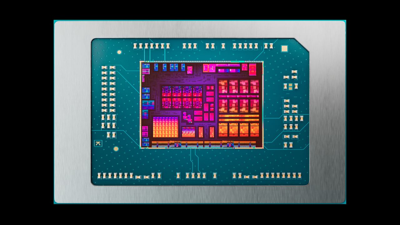
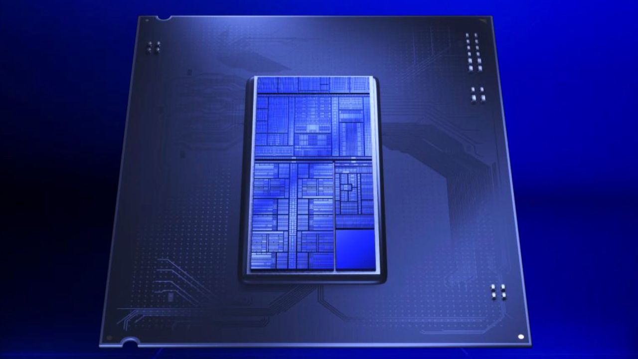
Intel's next-gen Nova Lake family of desktop CPUs is shaping up to be the company's most exciting launch in years, with a major performance leap expected across the board. A new leak from Jaykihn now claims that one of the SKUs from this lineup will have an iGPU so strong that it will require 65W of power delivery to achieve full performance. It will also apparently need two VCCGT phases to handle said power.
Preliminary.Nova Lake -S 12Xe SKU is shaping up to require a specific 65W-level PD segment for full graphics performance.It is the only segment demanding two VCCGT phases. https://t.co/pTzysqPN8FJuly 28, 2026
The SKU in question is a 16-core part composed of 8 P-cores, 4 E-cores, and 4 LP-E cores, while the iGPU is said to have 12 Xe3P cores. Just as a reminder, Xe3, also known as "Celestial," is an enhanced, optimized version of the Xe3 (Battlemage) graphics architecture that already debuted on Panther Lake. Similarly, Nova Lake is expected to use Coyote Cove P-cores and Arctic Wolf E-cores (and LP-E cores).
Top-end Panther Lake SKUs come equipped with the Arc B390 iGPU, which also has 12 Xe3 cores, so this Nova Lake SKU with 12 Xe3P cores should perform even better. Especially when you consider the thermal and power headroom at its disposal. AMD's desktop APUs, the Ryzen G-series, are usually 65W parts as well, but that's the TDP for the entire chip, not just the integrated graphics.
Requiring 65W of dedicated power delivery via two VCCGT phases would constitute a kind of top-end iGPU performance we haven't seen before. In fact, this rumored Nova Lake chip is arguably veering into Strix Halo territory where the up to 40 Compute Units on flagship SKUs can sip around 70W-80W of power. However, that's still a mobile part with an integrated SMU that can dynamically allocate power between the CCD and iGPU.
Nova Lake-S Rumored SKUs
SKU
Core Config (P+E+LP-E)
bLLC
TDP (Unlocked/Locked)
52 Cores (dual-tile)
(8+16)+(8+16)+4
288MB
175W
44 Cores (dual-tile)
(8+12)+(8+12)+4
264MB
175W
28 Cores
8+16+4
144MB
125W
28 Cores
8+16+4
-
125W / 65W
24 Cores
8+12+4
132MB
125W
24 Cores
8+12+4
-
125W / 65W
22 Cores
6+12+4
108MB
125W / 65W
22 Cores
6+12+4
-
125W / 65W
16 Cores
4+8+4
-
65W / 35W
12 Cores
4+4+4
-
65W / 35W
8 Cores
4+0+4
-
65W / 35W
6 Cores
2+0+4
-
65W / 35W
Nova Lake-S would likely use a traditional desktop rail split where the motherboard's VRMs must deliver up to 65W via two separate dedicated VCCGT phases (since one wouldn't be sufficient) to power the integrated graphics tile independently from the VCCCore CPU phases. That's unprecedented territory, and it serves as just one of many rumors from the Nova Lake launch that have us excited for the competition that's brewing for next year.
Current reports pin both AMD and Intel's next-gen releases to show up at CES 2027 instead of later this year. Therefore, take everything with a grain of salt; a lot could change between now and then, and we don't have confirmation on any SKU from Intel. The last time we saw Intel put out a strong desktop APU was 2015's Core i7-5775C, so a product like this has been a long time coming.
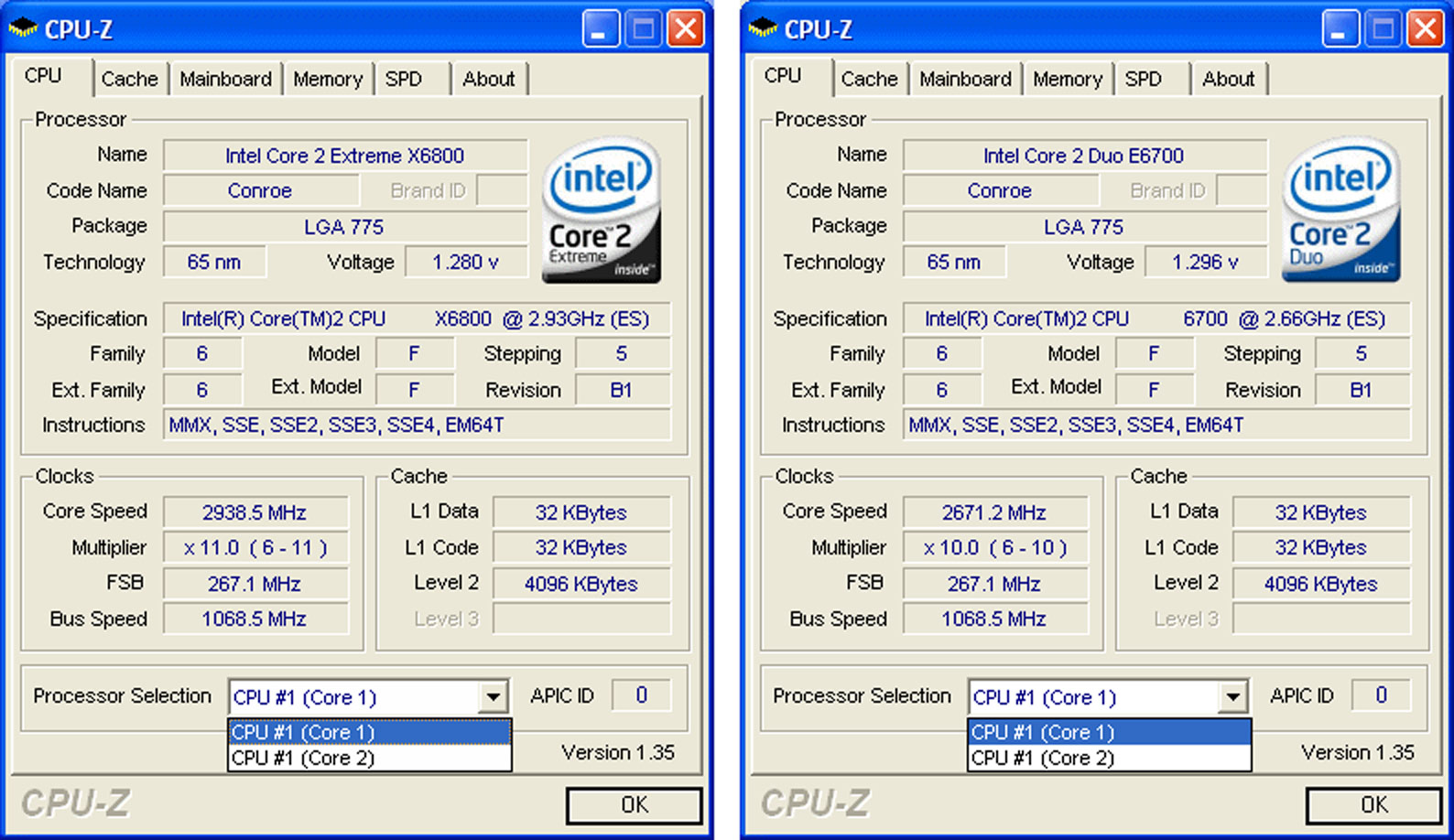
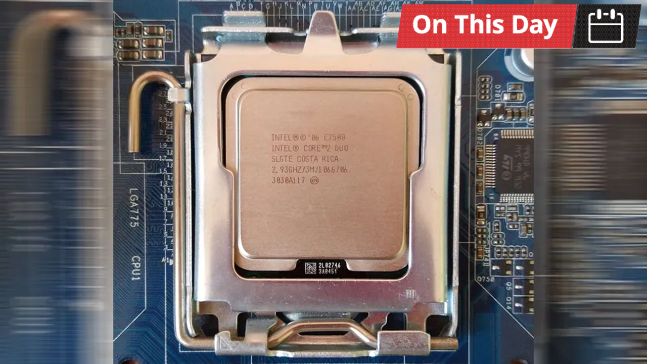
Today marks 20 years since the first raft of Intel Core 2 Duo processors, codename Conroe, was launched. Ten Intel Core 2 Duo and Intel Core 2 Extreme processors were unveiled for consumer and business desktop and laptop PCs and workstations on July 27, 2006. We were lucky enough to test Intel’s now legendary new desktop processors earlier in the month, and our reviewer anointed the Core 2 Duo “the new king.” Our early hands-on review underlined that “as soon as Core 2 Duo hits the market, it will outperform the complete Athlon 64 family (X2 and FX) in all areas, including gaming, where AMD has traditionally been very strong.”
The four mainstream and one high-end desktop Core 2 Duo processors that launched on July 27, 2006
Core 2 Model
Clock Speed
Multiplier
Front Side Bus Speed
L2 Cache
Extreme X6800
2,933 MHz
x11
266 MHz (FSB1066 QDR)
4 MB
Duo E6700
2,666 MHz
X10
266 MHz (FSB1066 QDR)
4 MB
Duo E6600
2,400 MHz
X9
266 MHz (FSB1066 QDR)
4 MB
Duo E6400
2,133 MHz
X8
266 MHz (FSB1066 QDR)
2 MB
Duo E6300
1,866 MHz
X7
266 MHz (FSB1066 QDR)
2 MB
The GHz race ends with an architectural revolution
One of the defining characteristics of the first Intel Core 2 Duo chips was that they kicked the GHz race to the periphery of the battlefield. After years of chips being sold with this performance statistic placed most prominently, Intel and the tech media had to educate the wider public that higher GHz numbers didn’t define performance.
Intel Conroe desktop chips came with a generational performance uplift we don’t see often. These third-generation dual-core processors from Team Blue would “provide up to a 40 percent increase in performance and are more than 40 percent more energy efficient versus Intel's previous best processor,” according to launch-day PR. Testers also observed that even the entry-level new Conroe chips could outpace the mighty flagship desktop Pentium Extreme Editions, despite running at nearly half the clock speed.
Behind the real-world performance successes Intel eagerly highlighted, and reviewers seemed genuinely excited by, there were a number of architectural innovations and refinements. Intel boasted that the Core 2 Duo contained “a whopping 291 million transistors” and had achieved many benchmark firsts in internal tests. Conroe arrived with higher efficiency, shorter pipelines, improved branch predictions, new shared Smart Cache, and substantially higher IPC, all built upon Intel’s newest 65nm process technology. With this attractive new price, it wasn’t difficult for Intel to retire its former king, with its hot, power-hungry, and big GHz Netburst architecture.
(Image credit: Tom's Hardware)
Defining the next decade+
With the Core 2 Duo, Intel regained its performance leadership from AMD and its Athlon parts. Conroe, the desktop Core 2 architecture, didn’t get singled out in our five best Intel CPUs of all time article (2024), but it was the direct ancestor of the legendary Core 2 Quad CPUs. These quad-core CPUs would take the Gillette-like next logical step with four cores on a chip, combining two Conroe dies in a single package, and launching in January 2007.
Moreover, from the mid 2000s onwards, multi-core became mainstream and developers seriously began to optimize applications and games for processors boasting more than just Core 0. Admittedly, single-threaded performance can still be important in Windows/apps/games in 2026.
To conclude, Intel’s Conroe would set the foundations for the firm’s CPU market dominance for more than a decade. Most would argue this successful run lasted all the way until the AMD Ryzen family matured and hit full stride with the Ryzen 3000 series.
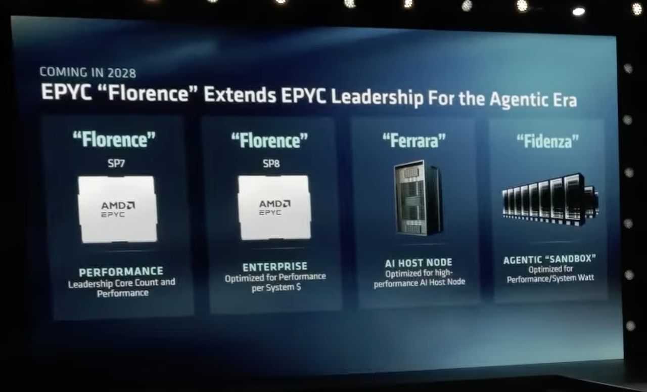
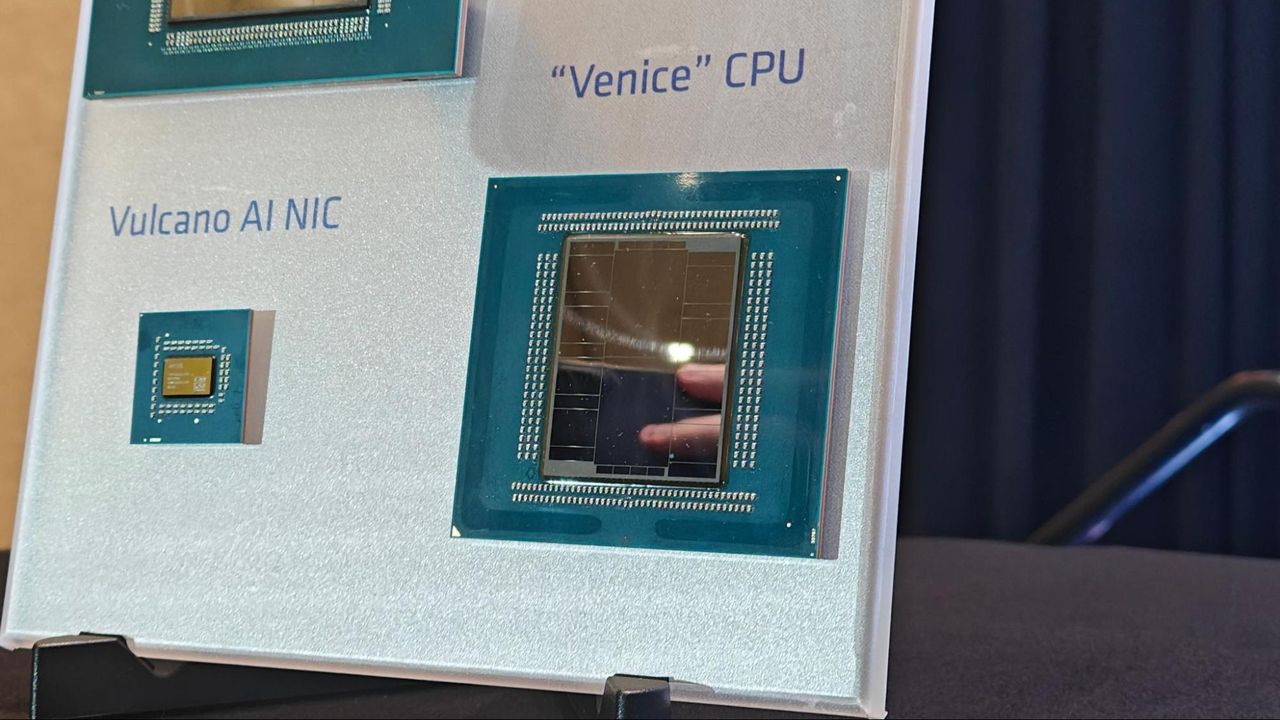
AMD used its recent Advancing AI 2026 event in San Francisco to launch sixth-gen EPYC "Venice" processors, Instinct MI400 Series GPUs, and Helios rack-scale systems, and to confirm that the Zen 7 generation arriving in 2028 will launch as three separate EPYC families rather than one.
The company named Florence, Ferrara, and Fidenza in its launch release, extended its annual CPU, GPU, networking, and rack cadence out to 2030, and put its total addressable market at roughly $2 trillion in 2030. It also introduced a competitive yardstick it hasn't used before, claiming the most AI agents per watt, per dollar, and per rack, though its own endnotes state those agent counts are estimated from CPU thread resources used as a proxy.
Three Zen 7 CPUs
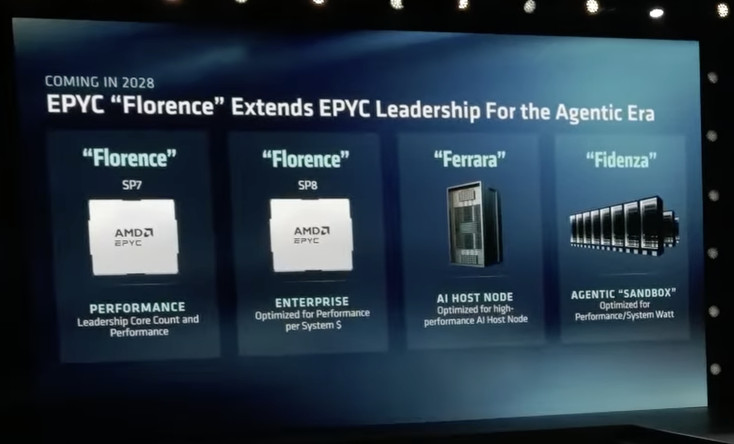
Florence carries fresh Zen 7 cores, a new set of AI compute extensions, and support for newer memory technologies, AMD chair and CEO Lisa Su said during the keynote. Ferrara is the AI host node portion, and it appears a second time further along the roadmap as the CPU inside the Helios 600 rack alongside MI600 Series GPUs and Pensando "Palma" and "Levanzo" networking. Fidenza, meanwhile, is the agentic sandbox product. AMD disclosed no core counts, no process node, and no socket for any of the three, and said only that Zen 7 uses leading-edge process technology.
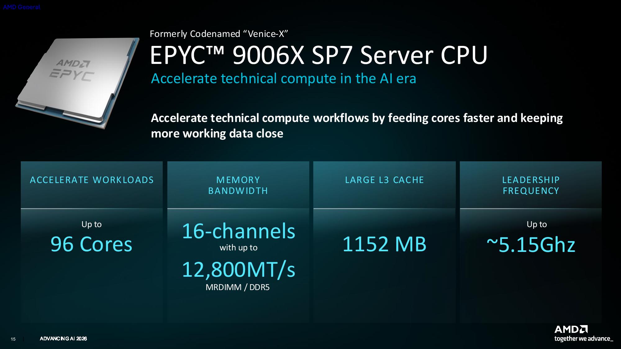
The fourth-gen EPYC generation, built on Zen 4, spanned Genoa, Bergamo, Genoa-X, and Siena across two sockets. The fifth-gen "Turin" generation then went the other way, folding Zen 5 and Zen 5c parts into a single 27-SKU stack on one socket with no separate cache-stacked or edge line at launch. Venice restarts the fan-out, with the 9006 series on the new SP7 socket now, and Venice-X arriving in 2027 with 1,152MB of 3D V-Cache, 96 cores, and a 5.15 GHz boost clock. Three named Zen 7 families at announcement, two years out, is a wider spread than AMD has ever opened a generation with.
AMD's own portfolio endnote describes the EPYC range as covering general-purpose enterprise, cloud, telecom, SMB, and HPC systems, plus, as a distinct category, sandboxed agentic AI deployments and GPU head node servers. Su told analysts in May that AMD was already working with customers on architectures beyond Venice, without naming categories at the time. The Zen 7 lineup puts a name to those two AI-specific segments for the first time.
Agents per rack
AMDAMDAMDAMD
AMD's main server CPU claim at the event is that sixth-gen EPYC enables the most agents per watt, per dollar, and per rack. Endnote 9xx6-012 in the launch release states that agent counts are estimates derived from available CPU thread resources used as a proxy under a consistent theoretical workload, and that real capacity varies with workload, model, memory, software, orchestration, and system configuration. The per-rack comparison behind it is core count at a 100 kW rack power envelope, pitting the 256-core EPYC 9996 against an 88-core Nvidia Vera, AMD's own 192-core EPYC 9965, and Intel's 128-core Xeon 6980P. The per-dollar metric is based on top-of-stack thread count divided by the 1,000-unit list pricing.
The per-watt comparison in that endnote lists Nvidia Vera at 450W and Arm's AGI CPU at 300W with one thread per core, alongside Intel's Xeon 6980P at 500W and AMD's EPYC 9965 at 500W. AMD had already claimed a 3.3 times rack-level advantage over Vera in June. Mercury Research put AMD at a record 46.2% of x86 server CPU revenue in Q1 2026, against 33.2% of units, and Arm-based designs took roughly 17.7% of server shipments in the same quarter, so the widening comparison shows where these units are going.
Starting with sixth-gen EPYC, AMD has replaced TDP with a figure it calls Default CPU Power, defined as total power consumed across the processor's compute and I/O dies at a stated performance target. AMD says both references can serve for product comparison and performance-per-watt analysis, and the endnote itself mixes the two conventions, quoting the EPYC 9956 at 400W Default CPU Power against TDP figures for the Nvidia, Intel, and Arm parts.
2030 cadence
Helios racks pair 72 Instinct MI455X GPUs with 18 Venice CPUs, 31TB of HBM4, and 1.4 PB/s of aggregate memory bandwidth, and are in production now. AMD claims up to 30% more inference tokens per dollar than Nvidia's Vera Rubin NVL72, based on AMD Performance Labs estimates from July 2026 using a Kimi K2 Thinking workload at 32K input and 8K output, with hourly GPU pricing projections. The 34-times token throughput gain AMD quotes for MI455X over MI355X comes from AMD's own measurements on DeepSeek V4 Flash at FP4. Both, however, are vendor-provided benchmarks with no independent verification yet.
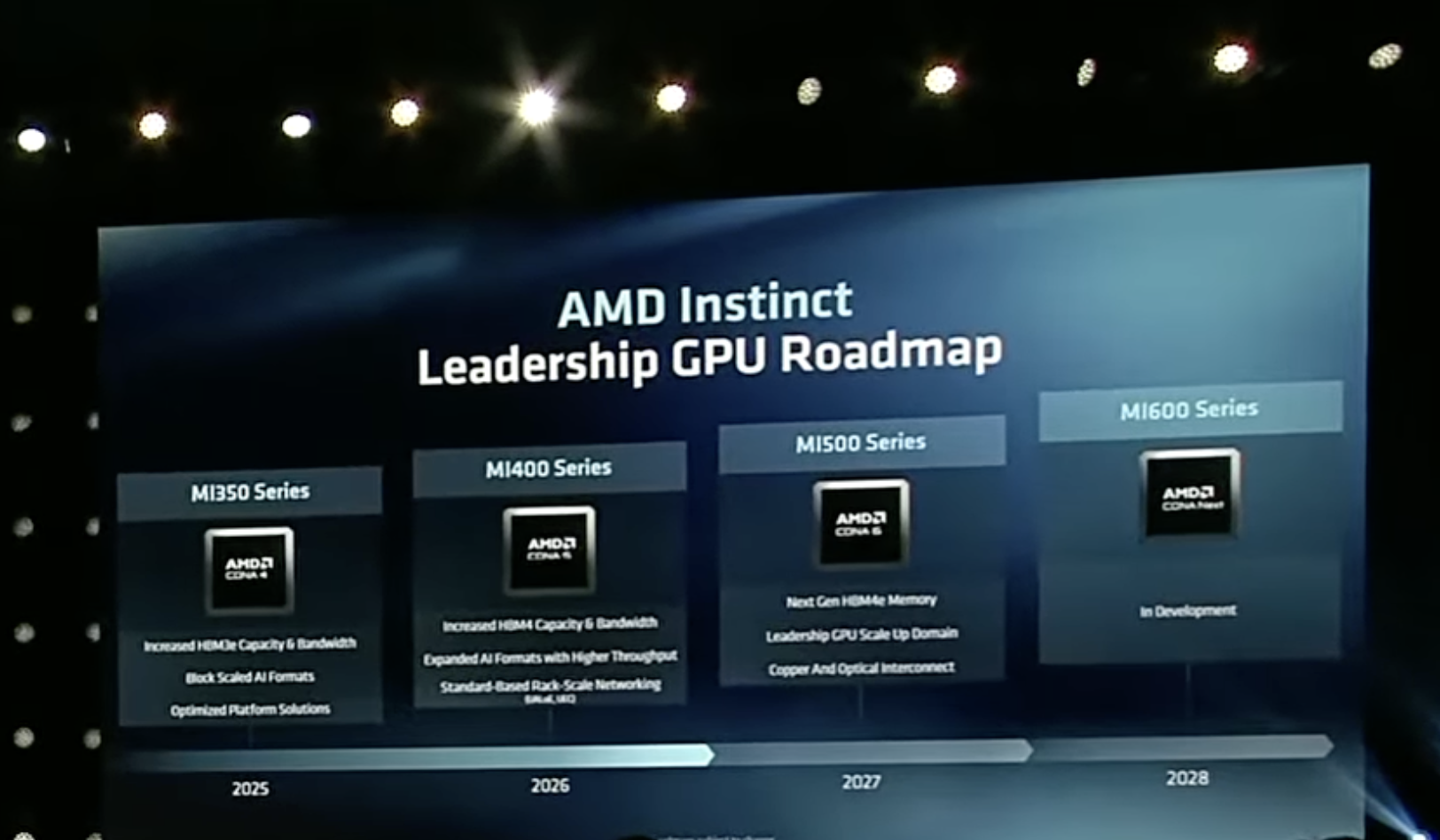
The forward roadmap runs MI500 Series GPUs in 2027 inside a Helios 500 rack built on EPYC "Verano" and Pensando "Como" and "Monza" networking, MI600 Series in 2028 inside Helios 600 on Ferrara, and Ravenna on Zen 8 in 2030.
OpenAI expects to bring Helios online from the fourth quarter of 2026, with deployments accelerating through 2027, while Meta is validating sixth-gen EPYC platforms in its labs and has begun testing Helios racks. Anthropic committed the day before the keynote to up to 2GW of MI455X GPUs in Helios systems, with the first gigawatt due in the first half of 2027. SemiAnalysis reported in February that manufacturing delays would push mass production and first production tokens on an MI455X UALoE72 system to Q2 2027; AMD software chief Anush Elangovan publicly rejected that assessment and said Helios remained on target for 2H 2026.
AMD's cautionary statement in the launch release lists the availability of essential components, naming memory supply specifically, among the risk factors that could cause results to differ from its projections. A Helios rack carries 31 TB of HBM4, and DRAM contract prices roughly doubled quarter-on-quarter in Q1 2026 before rising again in Q2.
FPGA and embedded systems expert Adam Taylor has recreated the U.S. Navy’s F-14 Tomcat’s Central Air Data Computer (CADC) in an FPGA. The CADC is famous for being the brains behind the F14’s advanced fighter capabilities including the control of the aircraft’s signature articulated sweep-wing system. So, what better way to test the new FPGA than in a 3D printed scale model of the F-14 Tomcat? Check out the video embedded below.
Fridays are for demos. We recreated the F14 CADC, it seemed only right we could test it with the actual swing wing feature. So we created a 3D printed F14 its first test. https://t.co/UUvebMIXei pic.twitter.com/3Mfcvo7PnqJuly 24, 2026
We wrote about the F-14 Tomcat’s CADC last year after discussions erupted on social media about whether this flight computer was actually powered by the "world’s first microprocessor." The brains behind the CADC were provided by the MP944. This chip lived in the shadows for quite some time, though. Despite the MP944 microprocessor beginning service in June 1970, over a year before Intel’s legendary 4004 would become available (November 1971) it was an official secret until 1998. Thus, the Intel 4004 managed to steal the limelight from the true first microprocessor, say those in the MP944 camp.
To recap, the MP944 was a 20-bit, pipelined, parallel multi-microprocessor melded with state-of-the-art MOS technology and ran at 375 kHz, executing 9,375 instructions per second. The flight-system powering chip, designed by Steve Geller and Ray Holt and a 25-strong team, also passed stringent ruggedness tests and was capable of running in temperatures spanning -55 to +125 degrees Celsius.
The MP944 worked as part of a six-chip system in the CADC, for the real-time calculation of flight parameters such as altitude, airspeed, and Mach number – and was a key innovation to enable the Tomcat’s articulated sweep-wing system. So it had to be performant, and some chip architecture enthusiasts assert that the MP944 was actually “8x faster than the Intel 4004.” Remember though, the Intel chip was originally designed for a far more humble desktop calculator.
3D printed F14 swing wing test
Getting back to Adam Taylor’s recent achievement, and we now have a full open source set of VHDL source code, documentation, and testbenches for an FPGA recreation of the F‑14’s CADC. The GitHub repo says the FPGA used was a Spartan-7 based SoM, part of the Adiuvo Embedded System Tile. The resource isn’t just the MP944 logic, Taylor includes complete synthesizable VHDL implementations for all six original CADC chips.
Intel on Thursday published its financial results for the second quarter of 2026, posting revenue of $16.1 billion — a 25% rise year-over-year — amid high demand for client and data center products. The company also said that due to extraordinary demand for its own CPUs, it will initiate mass production using its 14A (1.4nm-class) fabrication technology in 2028, which is in line with TSMC's plans for its A14 process technology.
"With encouraging external customer progress and increased demand for our internal products, we remain on track for 14A risk production for our internal products in the second half of 2027, and we made the decision in Q2 to fully commit to high volume ramp in 2028," said Lip-Bu Tan, chief executive of Intel, during the company's earnings call with financial analysts and investors.
Typically, companies initiate high-volume manufacturing (HVM) using a new process technology about a year after initiating risk production. Assuming that Intel intends to start risk production using 14A in the second half of 2027, it is reasonable to expect the company to start 14A HVM in the second half of 2028. It remains to be seen whether by the 'second half' Intel means July or December. If Intel initiates high volume ramp in November or December 2028, actual products made using the technology will emerge in 2029. In any case, Intel typically begins manufacturing using its leading-edge nodes in its development fab in Oregon and while it formally calls it HVM, actual volumes produced at such fabs are relatively low.
Another thing to note about Intel's 14A is that in 2028 it will start making its own products using this process, not products from external customers. Apparently, Intel still does not have any external clients that have committed to use the technology to make their products.
TSMC typically initiates production using its latest nodes in December and usually calls it the 'second half of the year.' Assuming that it follows the same pattern with A14 (though the progress of the node can enable the company to pull mass production in provided that customers' designs are ready), then the volume ramp will occur in 2029. TSMC claims that multiple customers have already taped out their ICs on A14.
Intel reported a strong second quarter as its revenue reached $16.1 billion, up 25% year-over-year and $1.8 billion above the midpoint of its guidance. Formally, Intel's GAAP losses reached a whopping $11 billion. However, this was driven by the $13.619 billion of mark-to-market losses on Escrowed Shares related to Intel's CHIPS Act Secure Enclave agreement with the U.S. government. Meanwhile, the company's non-GAAP net income was $2.2 billion, which reflects profitable underlying operations. The company's GAAP gross margin increased to 40.1%, up from 27.5% in Q2 2025. Intel's Operating cash flow totaled $7.0 billion, prompting the company to raise its capital spending outlook for both 2026 and 2027 as AI-driven demand continues to exceed available supply.
Intel's Client Computing and Physical AI Group (CCPG) generated $8.9 billion in revenue, up 13% year-over-year. The company confirmed that the CCPG result was not driven by increased unit sales, but was a result of higher average selling prices (ASP) due to supply constraints.
"Client obviously exceeded expectations. I would say it was largely ASP, of which some of that was mix related, some of that was our own like-for-like changes in ASPs where we thought we had seen some inflation on our cost and needed to pass that on to the end customer," said David Zinsner, chief financial officer of Intel, during the call.
The Data Center and AI (DCAI) business delivered the strongest growth as its sales climbed 59% year-over-year to $6.3 billion amid surging demand for Xeon processors, expanding AI infrastructure deployments, and rapidly growing purpose-built silicon sales.
"Q2 year-over-year server growth was the strongest on record, Xeon 6 continue to be one of the fastest ramping products in Intel history, reflecting improving execution and strong customer demand," Tan said.
"We also continue to see strong momentum in our purpose-built silicon product line, with revenue up roughly 20% sequentially and nearly tripling year-over-year," Zinsner said. "Purpose-built silicon revenue nearly tripled year-over-year."
Intel Foundry posted $5.8 billion in revenue, an increase of 31% year-over-year, as Intel 18A production ramped. At the same time the production units losses dropped to $2.1 billion — down from $2.4 billion in the previous quarter and $3.2 billion in the same quarter a year ago. External foundry revenue reached $293 million.
"Intel Foundry operating loss in Q2 was $2.1 billion and $348 million better quarter-over-quarter as higher yields improved cycle times and increased factory scale across Intel 4, Intel 3, and 18A drove improved wafer costs," Zinsner said.
Intel guided its third-quarter revenue to $15.8 billion – $16.8 billion and a projected non-GAAP gross margin of 42% and an EPS of $0.38.
A new 3D V-Cache-equipped CPU is reportedly in the works and could arrive as a mobile counterpart to the Ryzen 7 9800X3D. According to prominent tech industry insider Golden Pig Upgrade Pack on Weibo, the Ryzen 9 9800HX3D is expected to enter mass production in Q4 2026, with a potential launch at CES 2027. The chip is rumored to feature an 8-core, 16-thread configuration with boost clock speeds of up to 5.1 GHz, and 96MB of L3 cache.
It is also claimed that the processor was previously rumored to launch as the Ryzen 7 9755HX3D; however, it seems that the company might settle on the 9800HX3D. This essentially brings the branding in line with the desktop Ryzen 7 9800X3D. The chip could follow the same cache configuration with an eight-core CCD with 32MB of native L3 cache and a 64MB 3D V-cache stack.
Currently, AMD's most powerful 3D V-Cache-equipped mobile processor is the Ryzen 9 9955HX3D, featuring 16 cores, 32 threads, and a maximum boost clock of 5.4 GHz. It also offers a substantially higher L3 cache at 128MB and a configurable TDP of 55-75W.
While AMD hasn’t confirmed any details, the Ryzen 7 9800HX3D could likely be featured on premium gaming laptops that don't require the additional cores of the flagship 9955HX3D. An 8-core Zen 5 processor paired with 3D V-Cache could strike a better balance between gaming performance, power consumption, and overall system cost.
The rumored processor also aligns with AMD's recent approach of refreshing its X3D lineup instead of introducing new gaming CPUs. Similar to the recently announced Ryzen 9 9950X3D2 and the reintroduction of the 5800X3D, the 9800HX3D appears to build on an existing design while bringing AMD's latest branding and gaming-focused cache technology to another product tier.
The introduction of the 9800HX3D would also give laptop manufacturers a new gaming-focused option that is positioned below the flagship 9955HX3D. The processor would likely attract consumers seeking desktop-class gaming performance without paying the premium typically associated with 16-core mobile CPUs. As always, the rumored specifications and launch timeline should be treated with caution until AMD makes an official announcement.
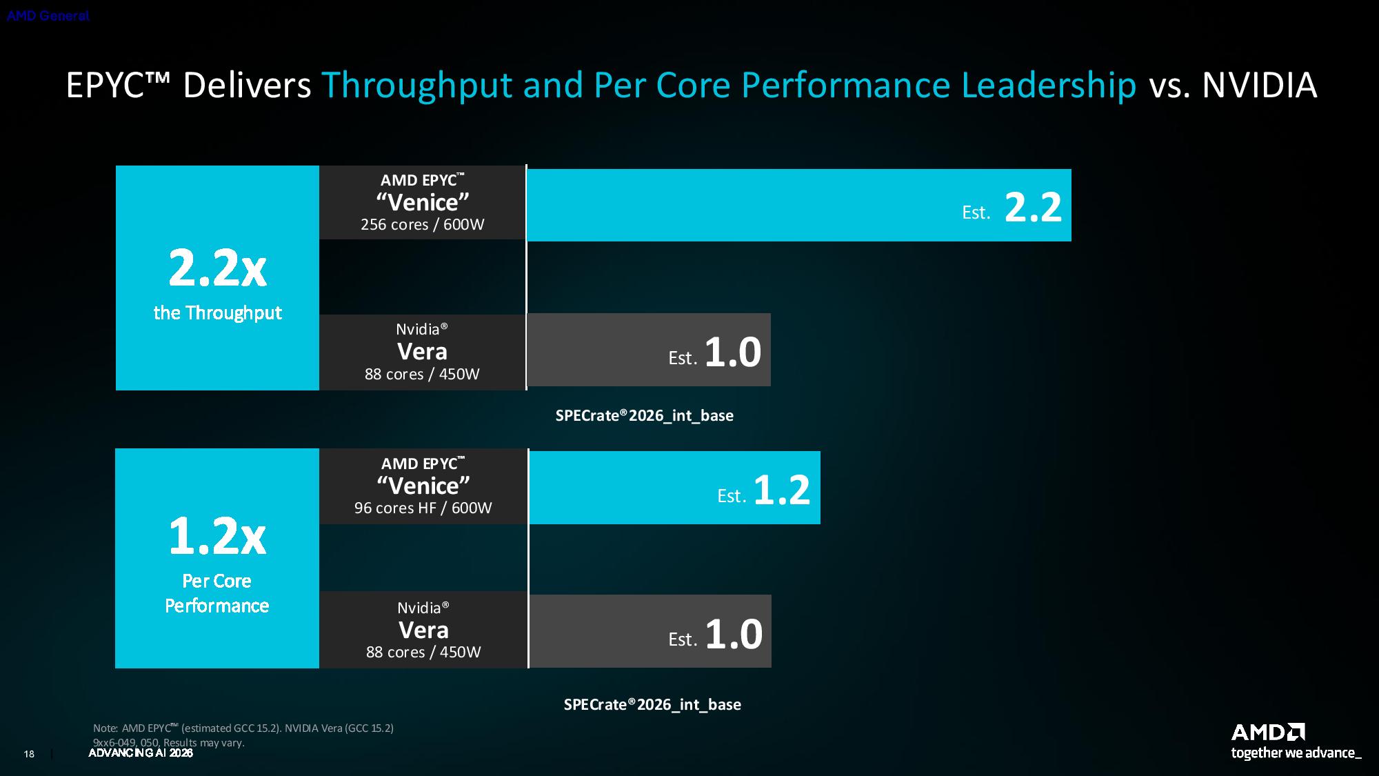
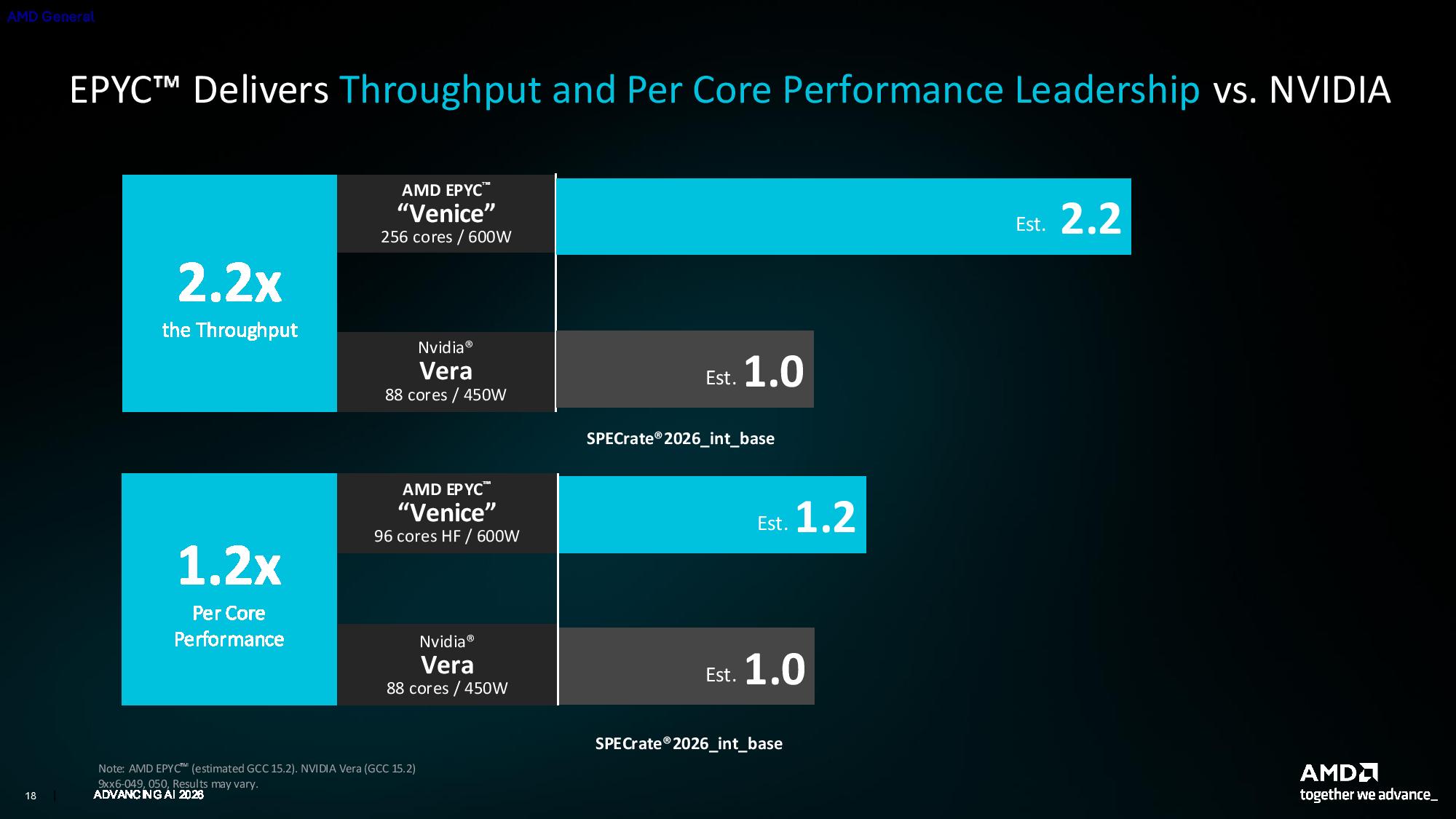
Although the industry has largely learned to move out of the way when the big green giant that is Nvidia steps into the room, one AMD executive said he was “very happy” to see Nvidia publish SPEC CPU 2026 benchmarks for its Vera CPU ahead of the Advancing AI 2026 event. AMD used the configuration in Nvidia’s white paper as a basis to run SPEC on its new Zen 6 ‘Venice’ CPUs, offering what it calls an “apples-to-apples” comparison between the two chips.
“We are very happy that Nvidia published their Vera performance [numbers],” said AMD’s Ravi Kuppuswany, corporate VP of compute and enterprise solutions. “We were actually being a little conservative. I actually thought we were beating them by smaller numbers than what I have here… we thought we’d have at least a 10% advantage. What we’re finding is… we have 20% advantage, and we have not even finished completely tuning.”
(Image credit: AMD)
Kuppuswany’s comments overlaid the slide you can see above, claiming 2.2x higher throughput with Venice compared to Vera, and 1.2x faster per-core performance. AMD has certainly stacked the deck in its favor here (as did Nvidia when it first published its Vera results), so let’s go through what this chart actually says.
As a quick aside, you’ll see “estimated” in the images above and below. These numbers aren’t guesses (they’re based on real runs), but SPEC maintains strict reporting guidelines for “official” runs. And because these runs aren’t reported to SPEC and therefore haven’t gained official status, they must come with the “estimated” disclaimer.
The throughput number is the easiest one to clarify. AMD compared its 256-core, 600W Epyc 9996 against the 88-core Vera, both in a 2P configuration. Yes, the CPU with more than twice the number of threads and an extra 150W stacked on top of its TDP has significantly higher throughput, as it should.
AMD would argue that it’s a fair comparison given that Nvidia is only offering Vera as a single, 88-core SKU. But the reality remains that the throughput comparison is one Vera could never win, and Nvidia would (and has) argued that it’s not trying to win in a race against the 256-core Venice. It’s building a single CPU for a single purpose.
The more interesting and consequential number here is the per-core performance. SPECrate_int is a throughput benchmark. A typical run loads all threads with a copy of an application and measures how much work gets done within a set amount of time. SPECspeed is the inverse of that, looking at a single application and how quickly it can run. AMD arrived at the numbers above by taking the overall SPECrate_int score and dividing it by the number of cores.
(Image credit: AMD)
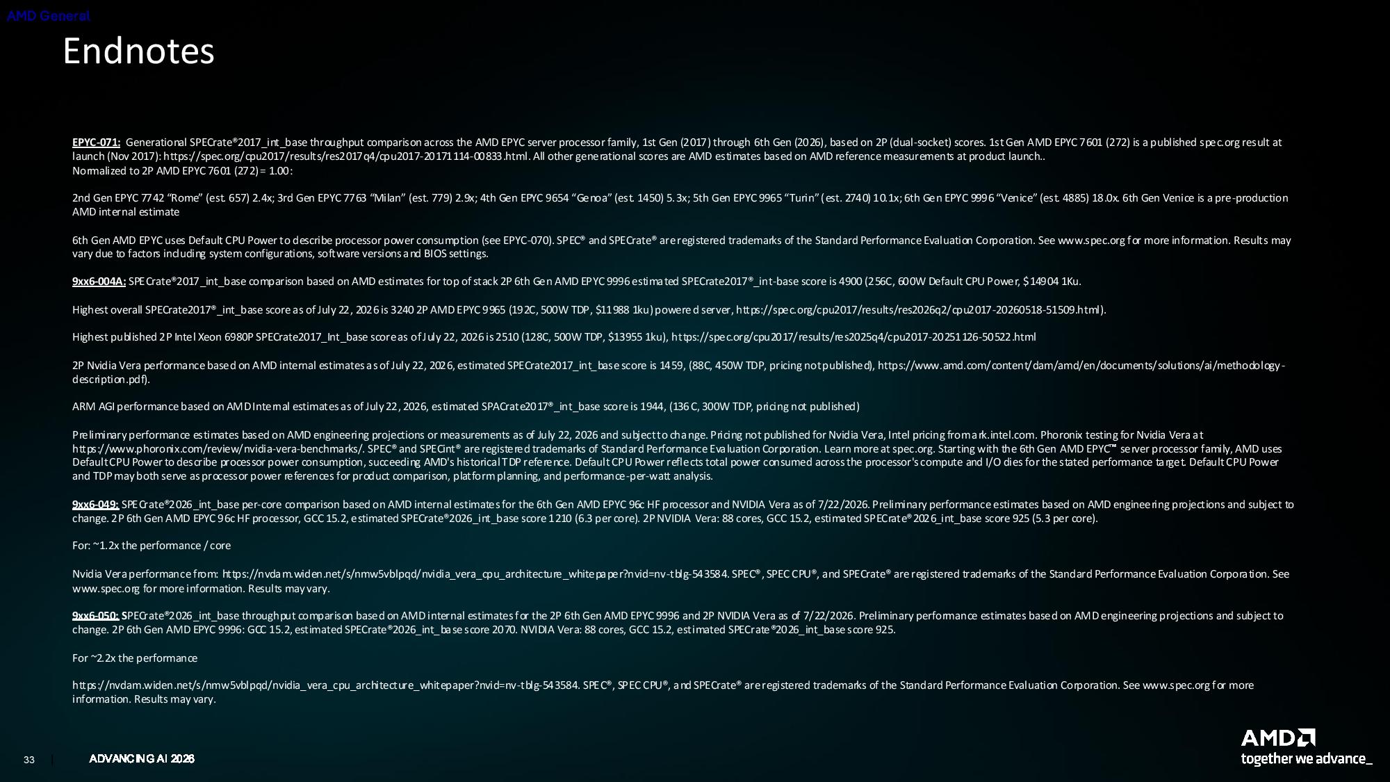
Nvidia’s results show Vera achieving a score of 925 overall. AMD says a 96-core High Frequency Epyc CPU achieved a score of 1,210. This processor, however, doesn’t seem to exist. AMD has the 96-core Epyc 9686F that boosts up to 5 GHz (much higher than the standard max frequency across the stack), but it has a rated TDP of 500W, not 600W.
Regardless, AMD divided that score by the number of cores; about 6.3 for AMD, and about 5.3 for Nvidia (remember these are 2P configurations). AMD says 1.2x, which actually translates to about an 18.8% lead. That’s not far off enough to say AMD was maliciously juicing its own numbers, but it’s important to note.
Given that AMD is using two different SKUs here (or maybe just one, considering the 9686F discrepancy), we can do the same per-core napkin math on the Epyc 9996 against Vera. Once again, Nvidia shared an overall score of 925, while the Epyc 9996 achieved a score of 2,070. That gives AMD a per-core score of 4.04.
That number isn’t important as a comparison point to Nvidia – again, we’re comparing a 256-core CPU to an 88-core one – but rather as a metric to see how Venice scales when normalized for per-core performance on a fully-loaded chip. That’s about 35% lower than the per-core score from the souped-up 9686F.
Although dissecting these numbers and sidelining the back-and-forth of two of the most powerful companies in the world is interesting, it’s not all that informative. SPEC maintains its strict reporting requirements for a reason. We won’t be able to say, with certainty, how these chips match up until we have official, reported runs. And even then, there’s an additional layer of compiler optimization (AMD and Nvidia both used GCC 15.2) and the broader context of the servers and workloads that these chips will serve.
The battle lines have been drawn, though only when looking at integer-based workloads. Vectorized performance is important, as well, and that’s an area where AMD holds a strong position in the current server CPU market. It doesn’t look like that will change with Vera, though we don’t have floating-point results to draw any conclusions from yet.
AMD has announced its long-term CPU roadmap, including multiple generations of its Zen microarchitecture at its Advancing AI event. Much of the event was focused on the new 256-core EPYC 9996 sporting the Zen 6 architecture, as well as Venice-X, which is slated to arrive next year. But AMD also teased a Zen CPU roadmap going out to Zen 8.
"In 2028, we are going to introduce Florence," Lisa Su, chief executive of AMD, said. "Florence brings the next-gen Zen 7 cores and its leading-edge process technology. It's a new set of AI compute extensions to really ensure that we have all of the AI capability, and it supports the latest memory technologies."
(Image credit: amd)
Su did not disclose specific details about the process technology, core counts, memory subsystem, or AI extensions planned for (Zen 7) Florence. However, she indicated that Florence will not be a standalone processor family, instead joined by the Ferrara AI host node and Faenza Agentic Sandbox for different AI workloads. AMD says this approach will enable it to offer purpose-built CPUs for a wider range of applications rather than relying on a single architecture configuration across the entire server market.
"And we are not stopping there," Su said. "We are already deep in development of Ravenna, our 8th Generation EPYC family built on Zen 8, and that family is already well under development for 2030."
The CPU roadmap is part of AMD's general strategy to offer a predictable cadence for its data center platforms.
(Image credit: amd)
On the accelerator side, the company is developing its MI500-series Instinct products with next-generation HBM, larger scale-up domains, and new copper and optical interconnect technologies, similar to Nvidia's outlook toward Rubin Ultra and Feynman.
"MI500 will deliver the largest generational leap in the history of Instinct, putting us on track to deliver more than 2,000 times higher inference throughput in just four years," Su said.
AMD also confirmed that its CDNA Next-based Instinct MI600 family is already deep in development for 2028. At the event, AMD launched its MI455X GPU, as well as teased more about its upcoming MI500X range, which we expect to launch next year.
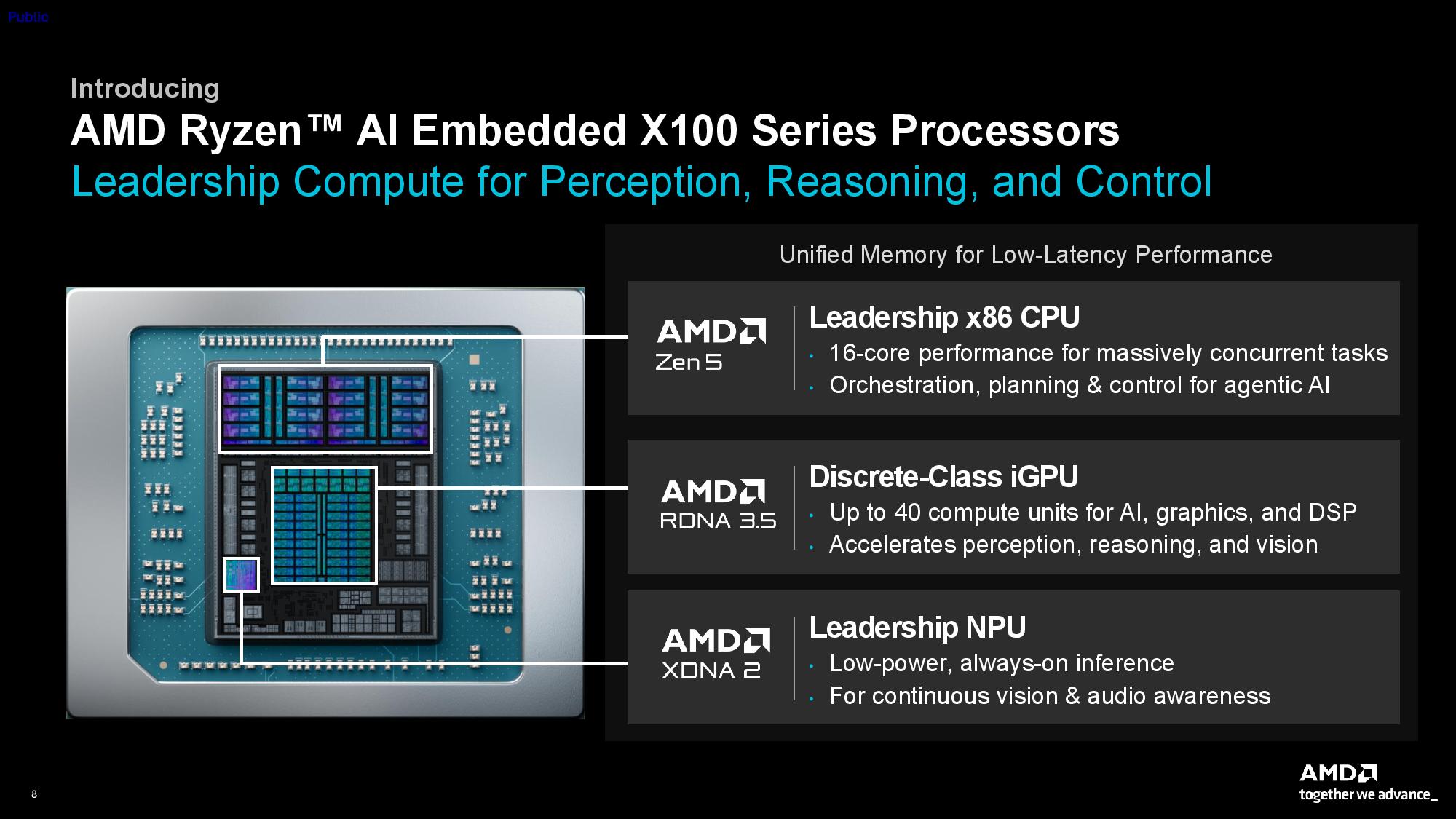
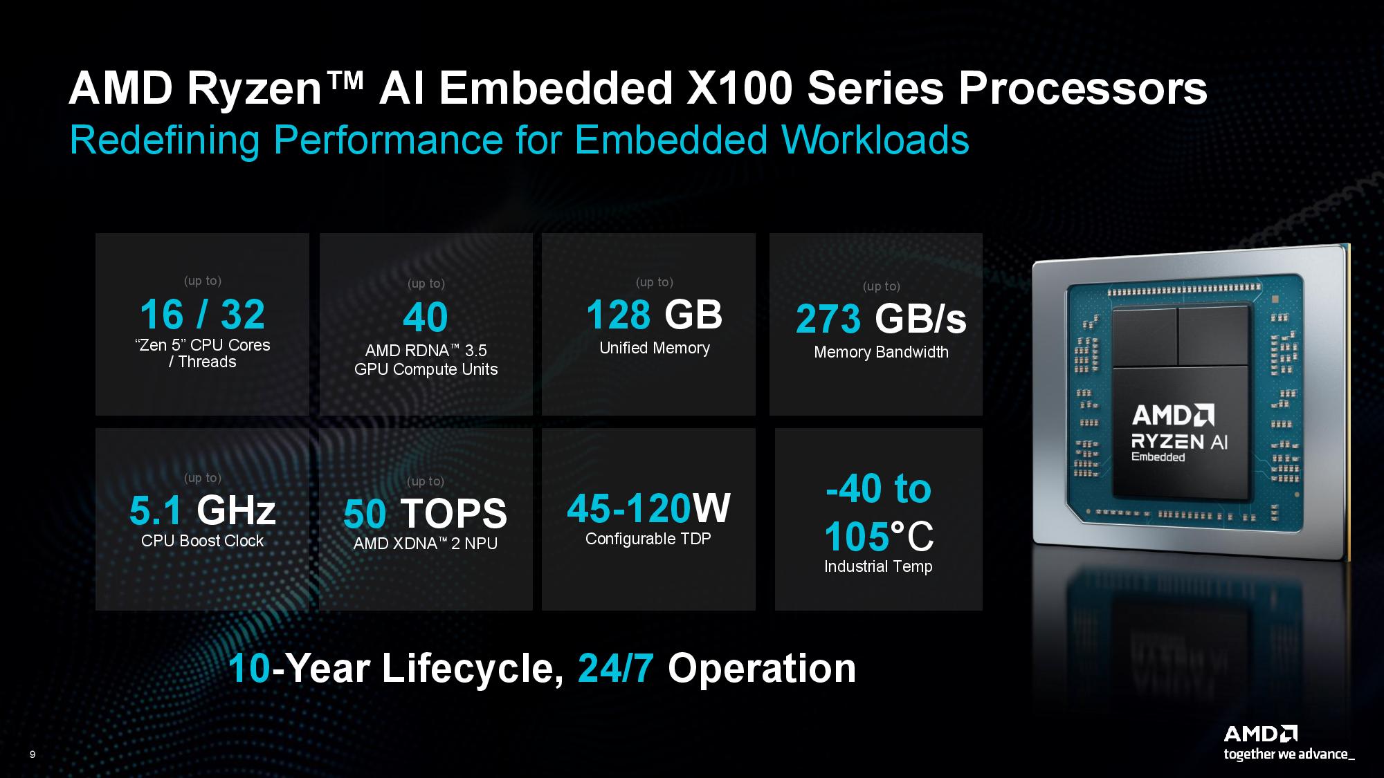
AMD is bringing its Strix Halo APUs into the world of physical AI. The new X100 series of processors come with similar specs as the various Ryzen AI Max models floating around in client devices, but they’re tailored for 24/7 operation, with a 10-year lifecycle in embedded applications like robotics.
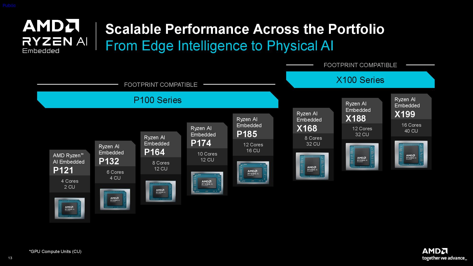
There are three SKUs that align with the three original Strix Halo models (not the updated versions with 40 CUs). The top-end X199 comes with 16 Zen 5 cores and 40 RDNA 3.5 CUs. The X188 steps down to 12 cores and 32 CUs, while the X168 comes with eight cores and the same 32 CUs. AMD hasn’t shared detailed specifications for each model, but the company says the range goes up to a 5.1 GHz boost clock and 128 GB of unified memory. They also include an XDNA 2 NPU with up to 50 TOPS, a configurable TDP between 45W and 120W, and operating temperature between -40 degrees Celsius up to 105 degrees.
AMDAMDAMD
AMD’s range bites back at Intel, which launched a range of Panther Lake SoCs for physical AI at the beginning of the year. Both make an argument for SoCs in robotics, reducing latency when the CPU, AI accelerator, and memory are fragmented across separate chips. The X100 range is just physically larger than Panther Lake, packing much more silicon on the SoC for more powerful deployments.
(Image credit: AMD)
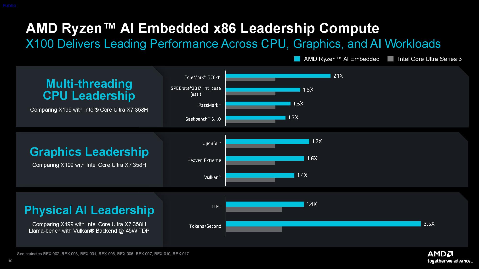
The company shared a range of benchmarks comparing the flagship X199 against Intel’s Core Ultra X7 358H, a 16-core chip with Intel’s Arc B390 iGPU that has 12 Xe3 cores. AMD claims a lead of 1.2X and 1.3X, respectively, in GeekBench 6.1 and PassMark, as well as 1.5X in an unofficial SPECrate 2017 run looking at integer workloads. In graphics, AMD unsurprisingly takes the edge with 1.4X faster Vulkan and 1.7X faster OpenGL performance (both measured with GFXBench 5 on Ubuntu), as well as a 1.6X lead in Unigine Heaven Extreme.
On the physical AI front, AMD claims a 1.4X improvement in Time to First Token (TTFT) and 3.5X faster tokens per second in Llama-bench, with a Vulkan backend running at a 45W TDP. These results need a massive dash of salt, however.
AMD tested the Ryzen AI Max 395+ “configured to reflect Ryzen AI Embedded X199 specifications.” It tested on the Maple reference board with a 5.1 GHz CPU clock, 2.9 GHz GPU clock, and sustained 45W TDP. The X7 358H, meanwhile, was tested in an MSI Prestige 16 Flip AI+ with an enforced TDP limit of 30W. AMD then “projected” 45W performance on the Intel chip “using scaling factors derived from public benchmark data.”
It’s not exactly an apples-to-apples comparison, in other words. There’s some sort of proxy stand-in or extrapolation of data across all of the benchmarks here, so keep that in mind as we work through the rest of AMD’s X100 announcements.
AMD X100 Kria SOM and robotics developer platform
Tom's HardwareAMDAMDAMD
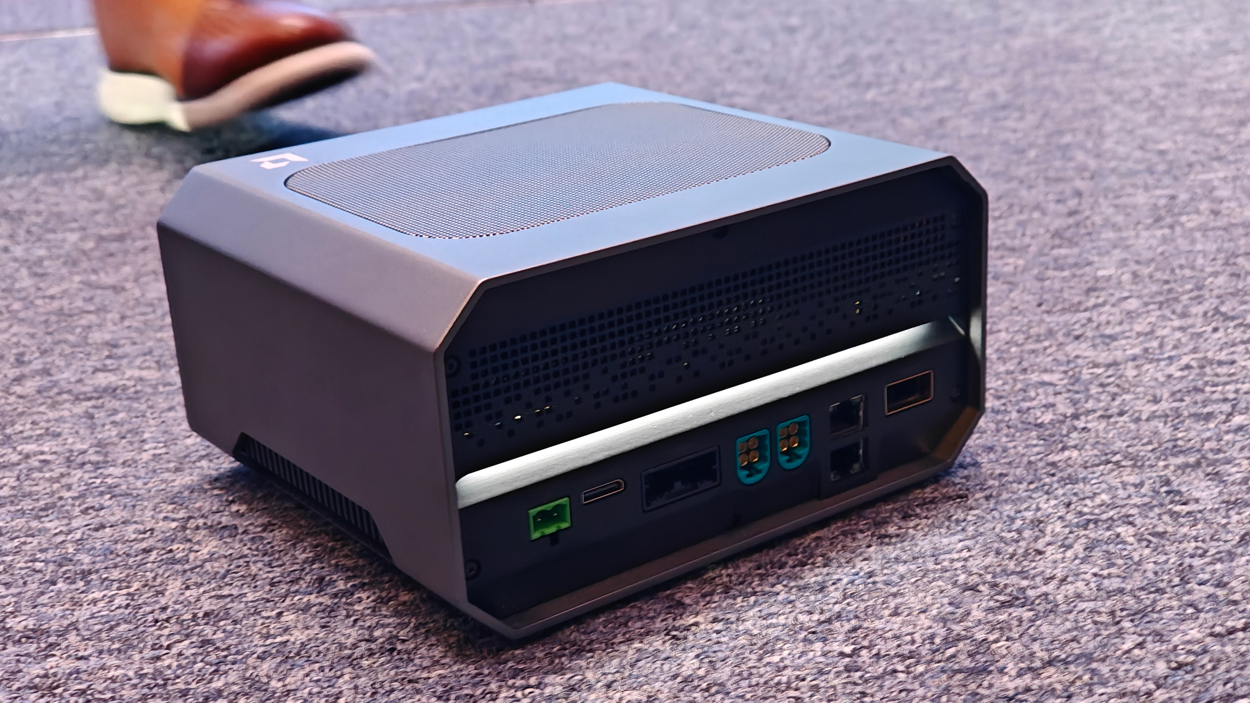
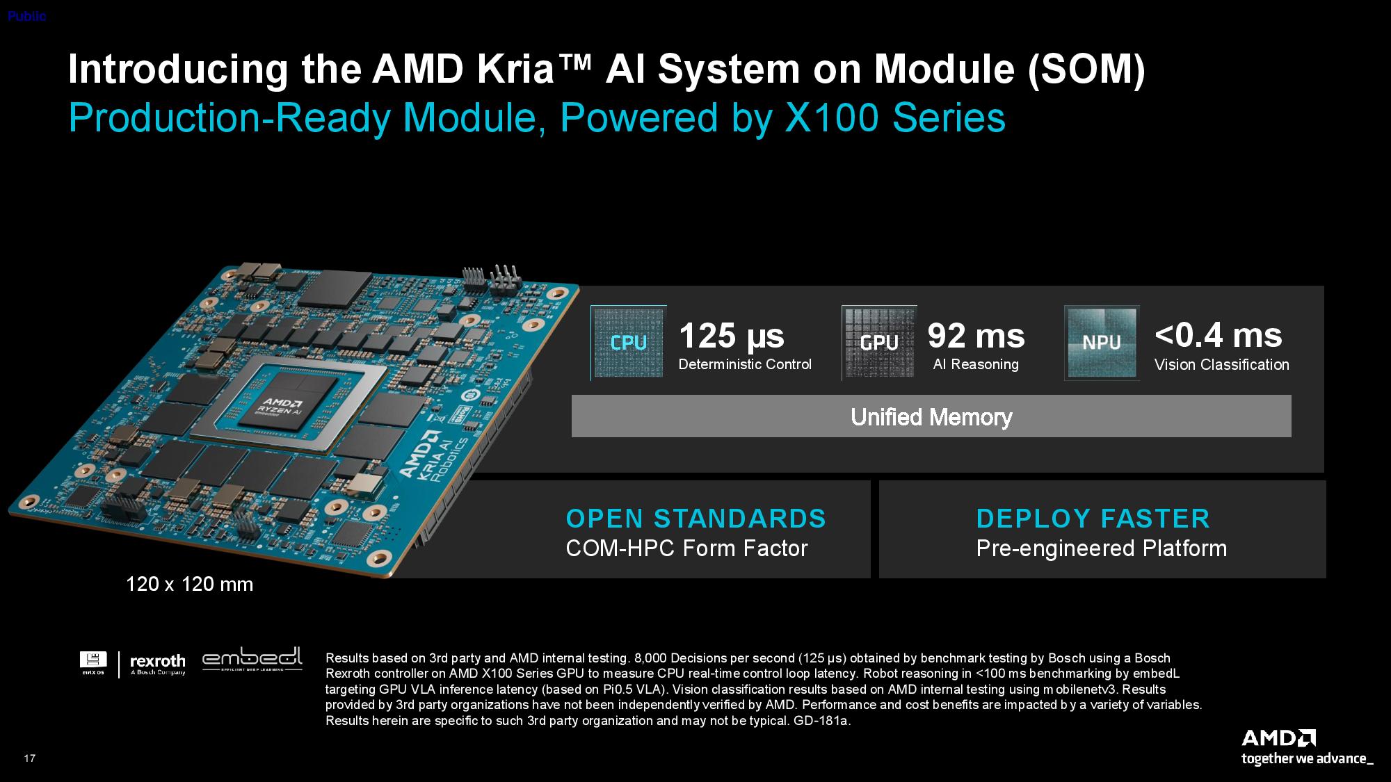
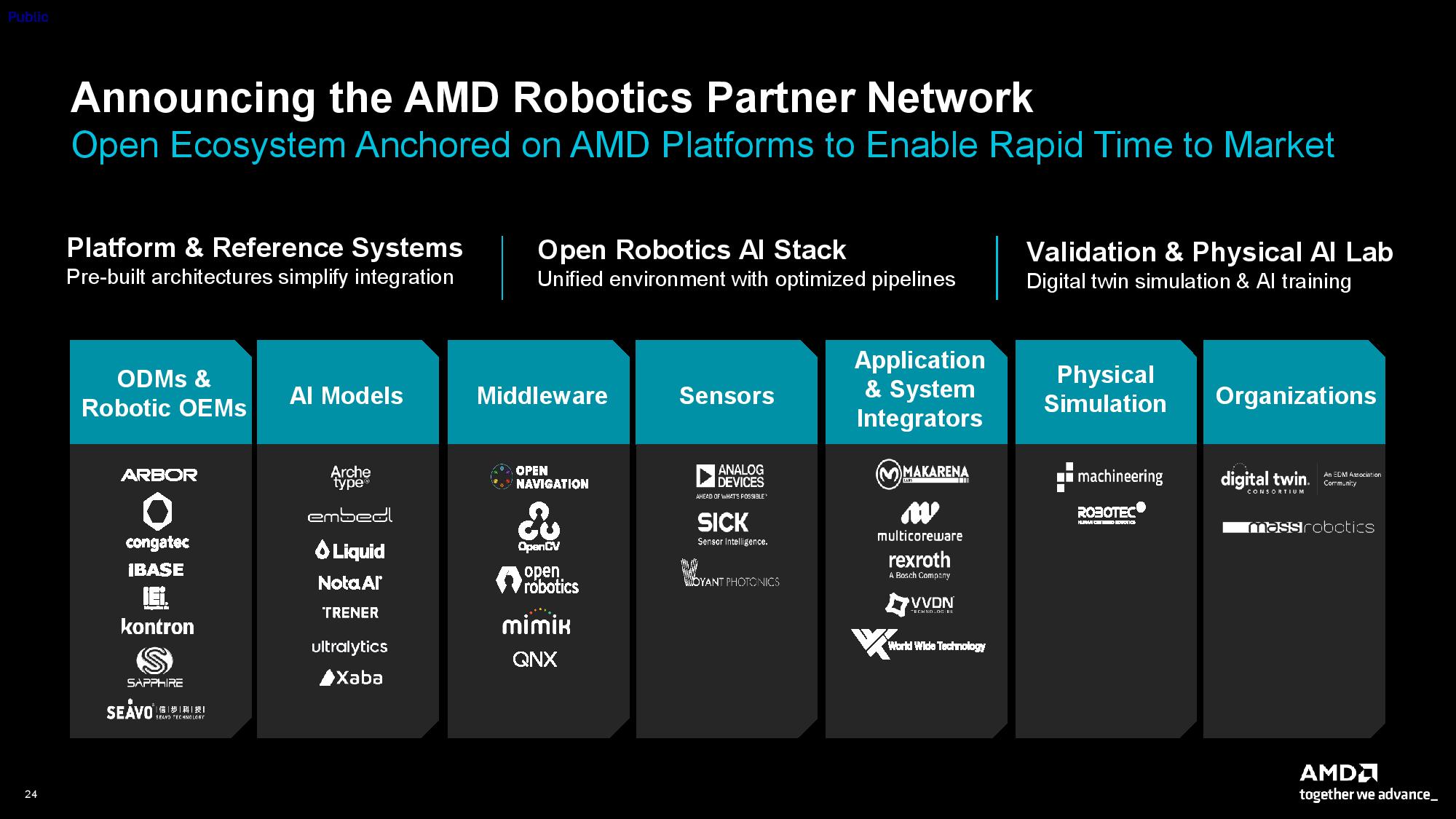
utside of the chips themselves, AMD is offering X100 models as part of a Kria System on Module (SOM) or an integrated robotics developer platform. The Kria X100 board measures 120mm x 120mm and conforms to the standardized COM-HPC form factor. If you’re a developer that wants to develop for the board, AMD is offering its Kria AI robotics developer platform.
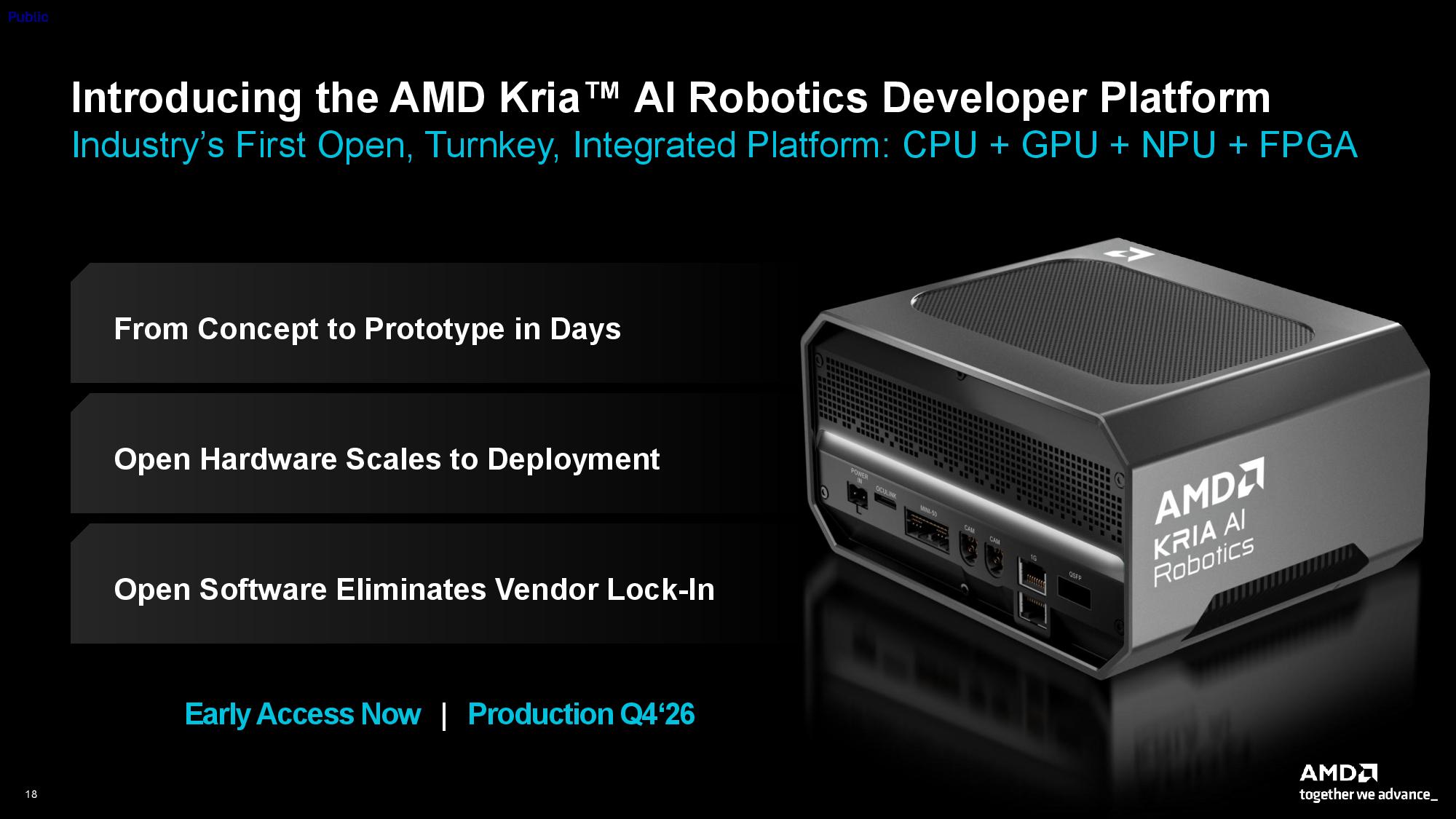
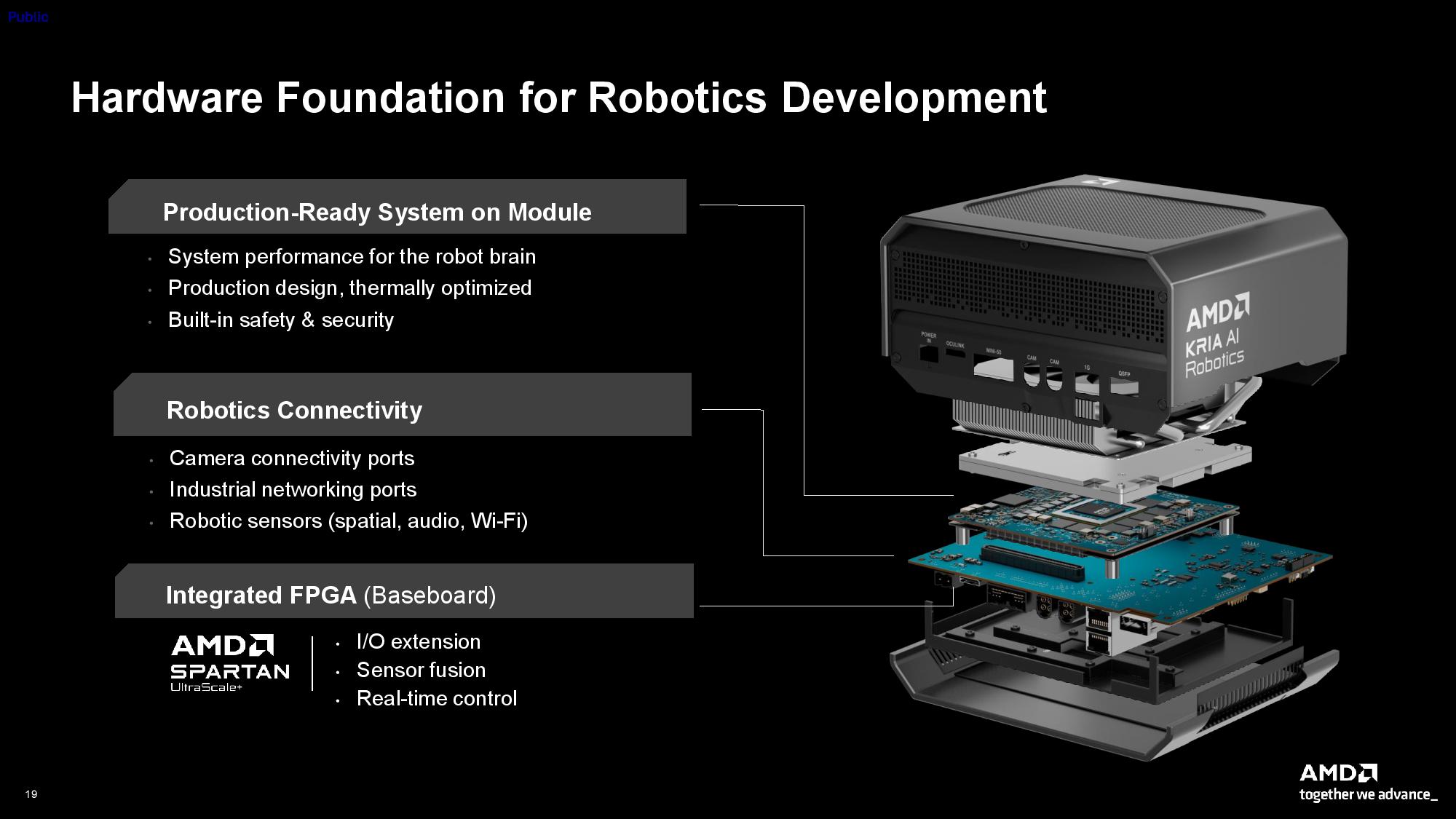
It’s a fully-integrated box, leveraging the X100 Kria SOM alongside AMD’s Spartan UltraScale+ FPGA baseboard. AMD says it’s a “turnkey” solution for robotics development, including specialized connectivity for cameras and industrial networking, along with robotic sensors. The platform is available in early access now, and AMD says it’ll be in full production in Q4 of this year. .
(Image credit: AMD)
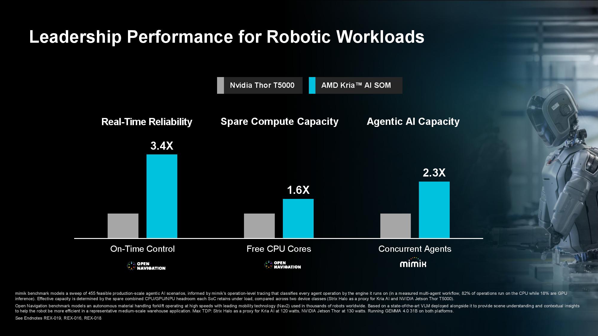
AMD shared some benchmarks for the X100 Kria, as well, comparing it to Nvidia’s Thor T5000. These benchmarks weren’t run internally at AMD. They were commissioned by AMD and ran by Open Navigation and Mimix. Critically, the benchmarks didn’t test an X100 Kria board, or at least, not exactly in the form it will take once it’s inside a robot or AMD’s developer box.
Instead, AMD is comparing Nvidia’s Jetson AGX Thor developer kit to a GMKtech EVO-X2 AI mini PC with a Ryzen AI Max+ 395 “configured to reflect Ryzen AI embedded x199 specifications.” Naturally, the thermal and power environment of these chips will heavily influence performance.
AMDAMDAMDAMD
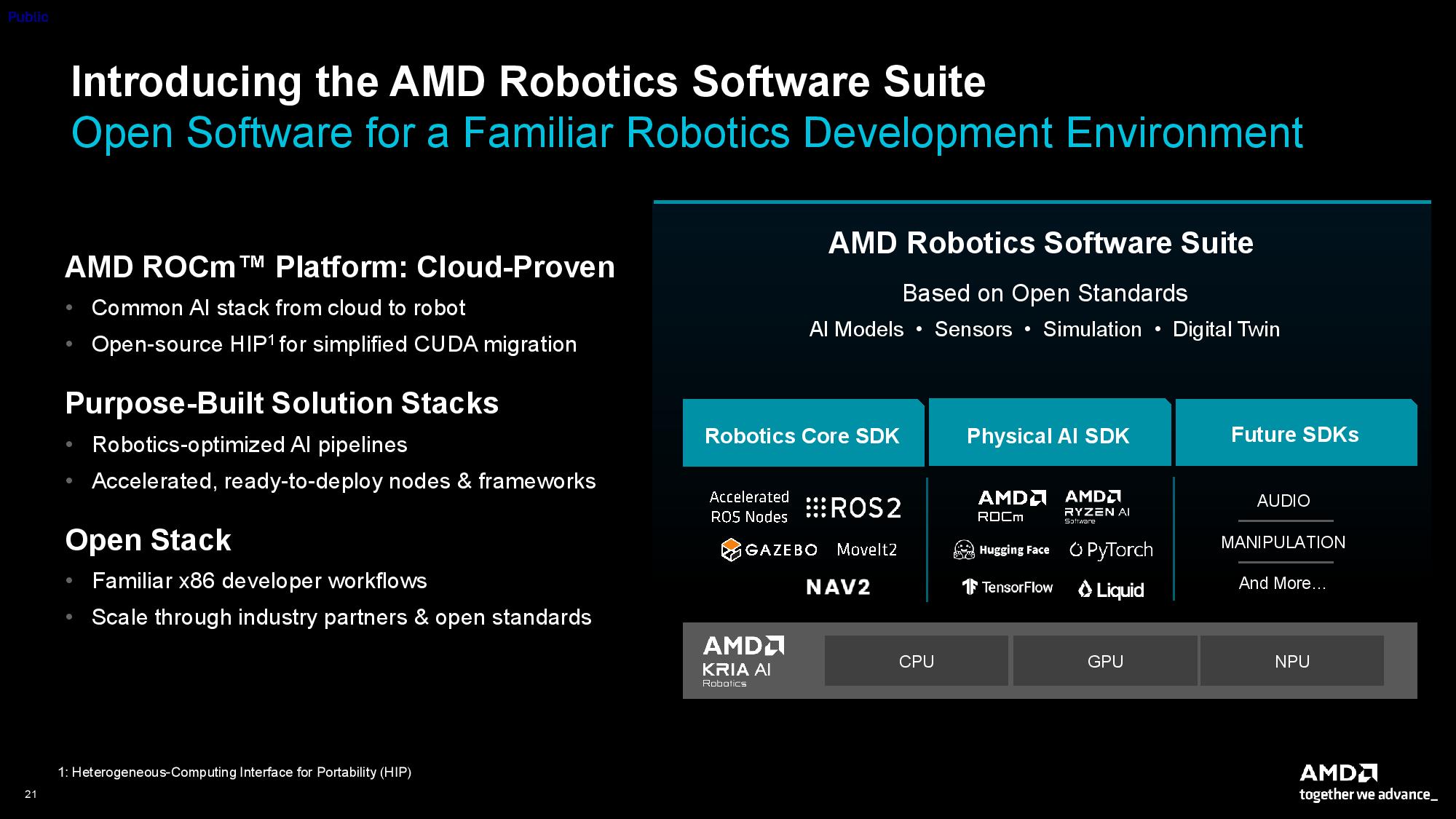
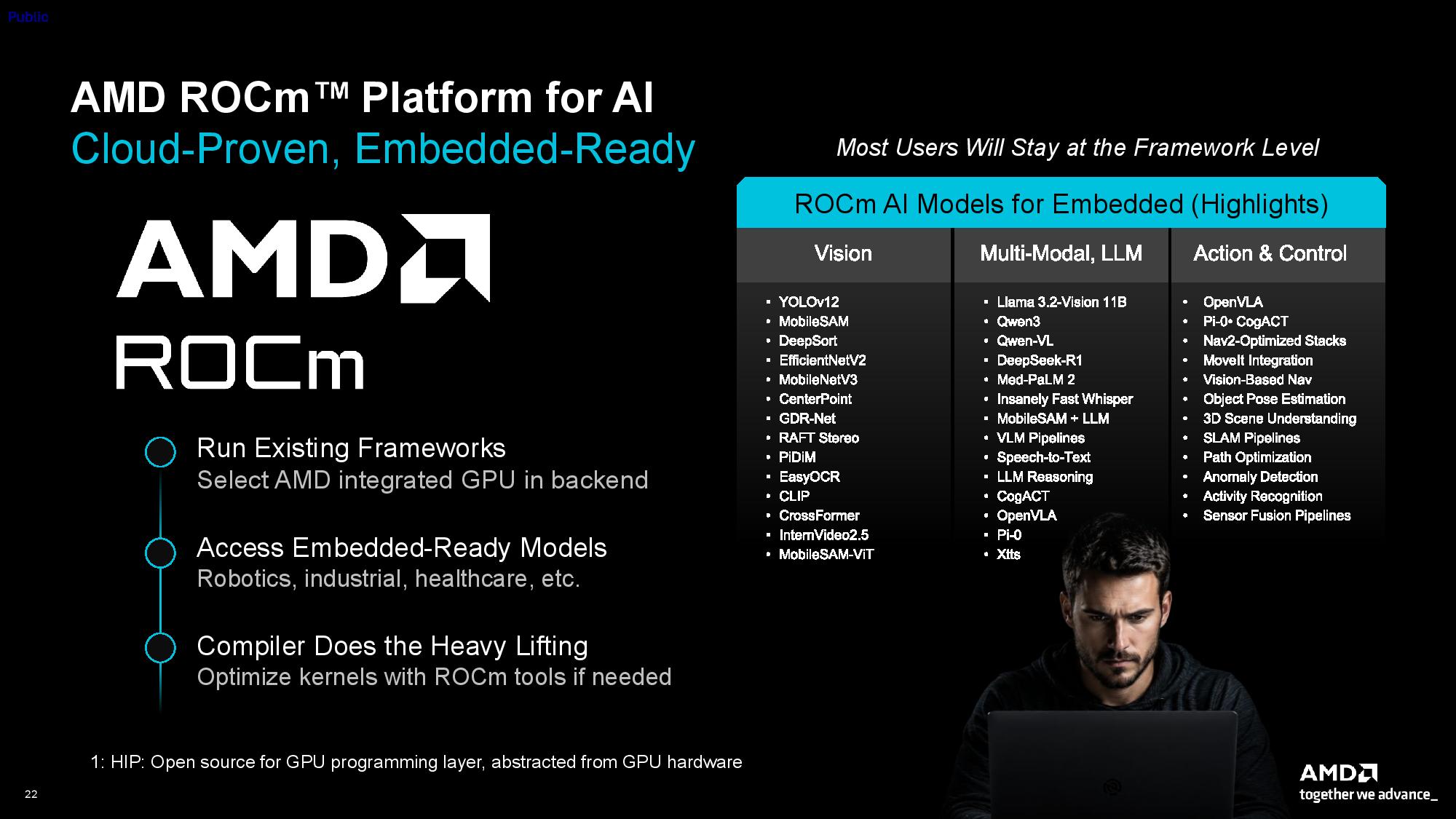
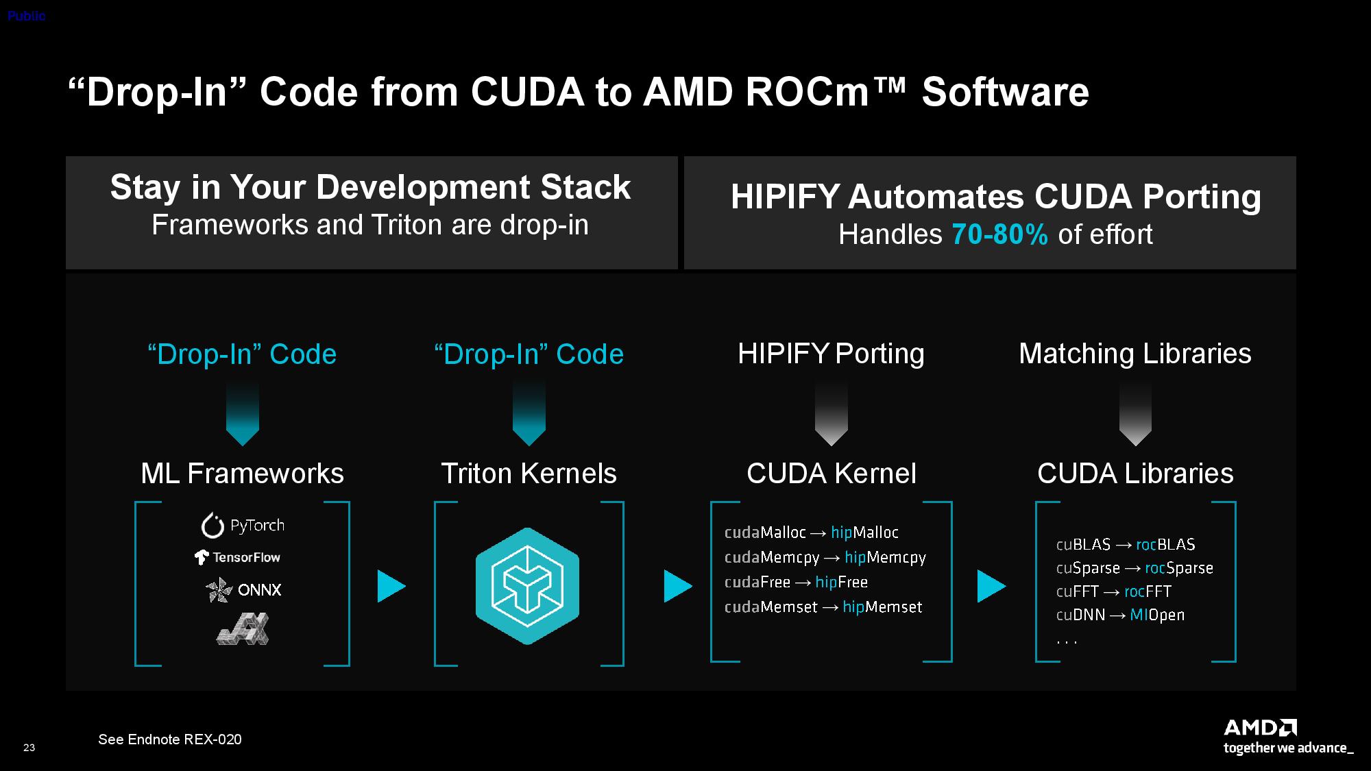
AMD is continuing its attempt to siphon developers away from Nvidia’s CUDA platform for development, as well. It’s HIPIFY tool converts CUDA code to AMD’s HIP C++ portable code, and the company claims it can now handle 70-80% of the “effort” of porting on its own. AMD tested on a Ryzen AI Max+ 395, once again configured to match the X199, and it ported 15 CUDA applications, comprising 1,199 lines of code, to arrive at that 70% to 80% range.
X100 Kria lives at the “brain” of the robotics platform, but AMD envisions an end-to-end solution for humanoid-style robots with its Spartan UltraScale+. Zynq UltraScale+, and Versal AI Edge Gen 2 FPGAs and SoCs
AMD is finally providing some details on its first Zen 6 CPU, which it has been teasing for over a year. The Epyc 9996 is a 256-core / 512-thread chip, packing AMD’s new Zen 6 architecture, and it’s the first to launch in what AMD describes as a “broad portfolio” for Venice. In addition to claiming significant performance advantages over the impending Nvidia Vera and Intel’s Xeon 6, AMD says it will continue to build out the Venice range with bespoke designs over the next year.
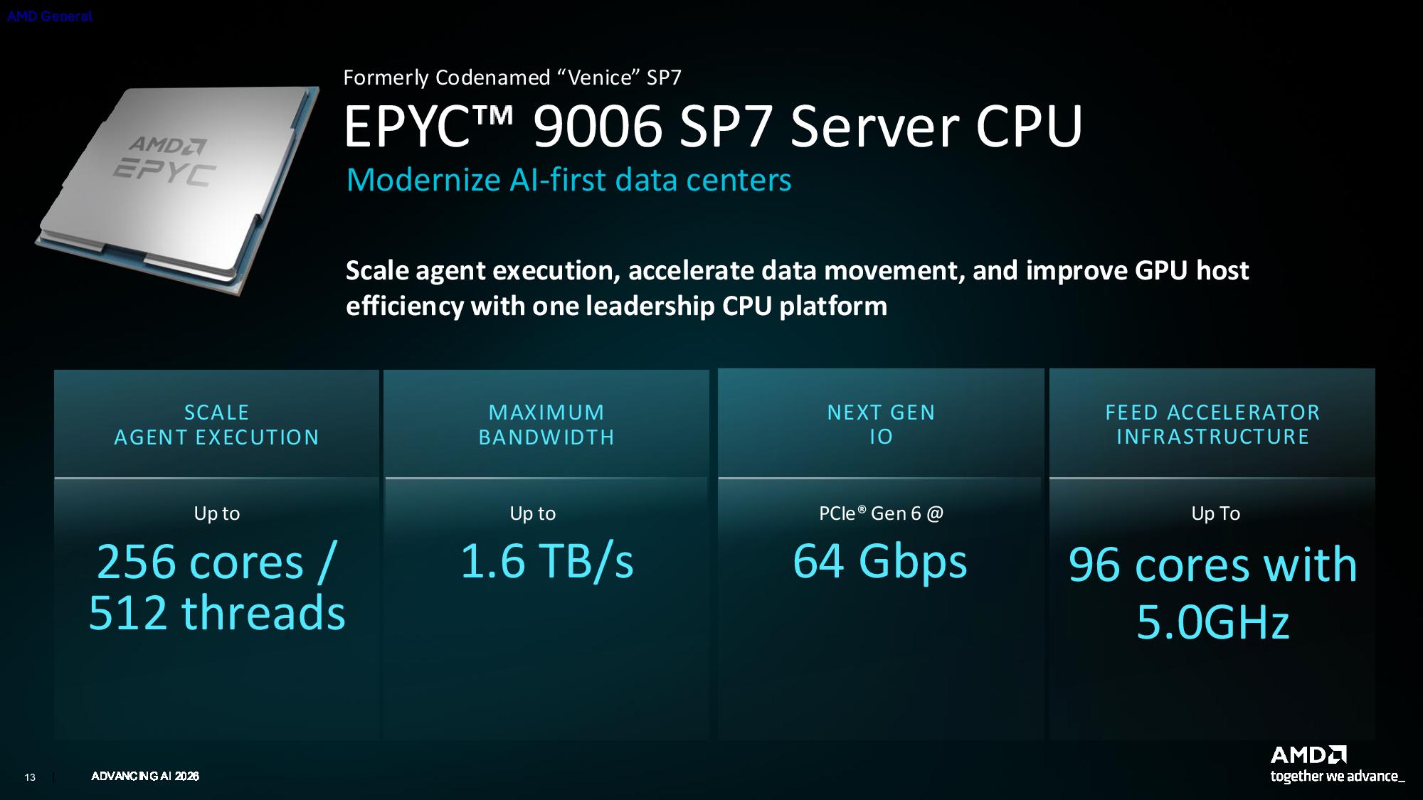
“It’s not just a single processor,” said AMD’s Ravi Kuppuswany, corporate VP of compute and enterprise solutions.q “It’s a portfolio.” AMD says it has purpose-built solutions, splitting its offerings depending on the application, not dissimilar to how Intel has split its Xeon ranges over the past few generations (nor how AMD has softly segmented its Epyc offerings). The roadmap starts with the main Venice lineup on the SP7 socket, which is what AMD has been teasing for so long. It scales up to 256 cores and 512 threads, 1.6 TB/s of memory bandwidth with fast MRDIMMs, and 128 PCIe 6 lanes in 1P configuration (160 lanes in 2P).
AMDAMDAMDAMD
Note: When scaling up to 256 cores, AMD uses its Zen 6c “dense” design. With a standard Zen 6 design, AMD says Venice scales up to 128 cores and 256 threads, while high-frequency variations top out at 96 cores.
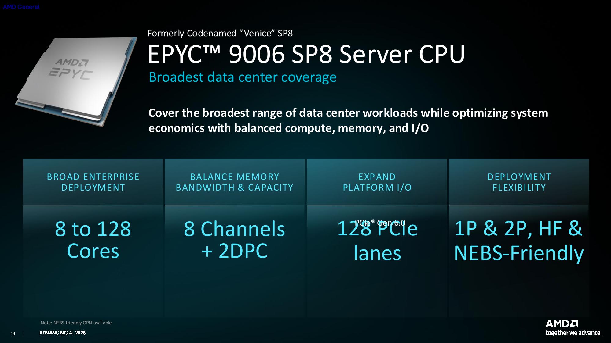
In the first half of next year, AMD plans to launch Venice on its SP8 socket, offering as few as eight cores and up to 128, focused on smaller deployments. These chips support eight-channel memory with two DIMMs per channel, and the same 128 PCIe 6 lanes.
Venice-X is expected in the second half of 2027, on the SP7 socket. We didn’t see Turin-X, but the last, last-gen Genoa-X came with 96 cores and up to 1152 MB of stacked L3 cache. Those specs haven’t changed (short of the Zen 6 microarchitecture), but AMD says it's able to clock Venice-X up to 5.15 GHz.
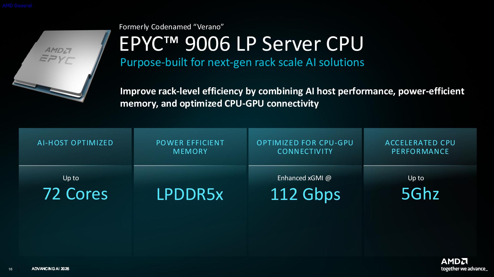
Finally, Verano should arrive in the second half of next year on the SP8 socket, and it looks like the most direct competitor to Vera (AMD’s Kuppuswamy had some fun with calling it “Vera-No”). It’s optimized to be an AI host node, says AMD, packing up to 72 cores and 5 GHz peak clocks. Critically, it comes with a 24-channel LPDDR5X memory system, leveraging SOCAMM2 modules.
AMD Epyc 9006 SP7 specifications
Chip
Cores / Threads
Base / Boost Clock (GHz)
L3 Cache
TDP
Epyc 9996
256 / 512
2.55 / 4.1
1024 MB
600W
Epyc 9966
192 / 384
2.9 / 4
768 MB
600W
Epyc 9846
168 / 336
2.85 / 3.7
768 MB
500W
Epyc 9756
128 / 256
3.15 / 4
512 MB
500W
Epyc 9G76
96 / 192
3.4 / 4.8
384 MB
500W
Epyc 9656
96 / 192
3.05 / 3.7
512 MB
400W
Epyc 9686F
96 / 192
3.4 / 5
384 MB
500W
Epyc 9556
64 / 128
2.75 / 4.3
384 MB
300W
Epyc 9586F
64 / 128
3.75 / 5
384 MB
500W
One of the advantages Nvidia claims with its Vera chip is lots of memory bandwidth through the LPDDR5X system. AMD’s approach is different with Venice SP7. It’s scaling up to 16-channel memory with Venice SP7, with support for MRDIMMs running at 12,800 MT/s, or standard DDR5 RDIMMs running at 8000 MT/s.
It’s a significant jump over Turin, which uses 12-channel memory, with support for RDIMMs running at 6400 MT/s. AMD claims per-socket bandwidth of 1.6 TB/s, significantly higher than the 1.2 TB/s available on Vera, and nearly triple the 576 GB/s per-socket bandwidth of Turin. Intel recently enabled 8000 MT/s RDIMMs on select Granite Rapids and Clearwater Forest SKUs, and it says support for MRDIMMs with speeds up to 8800 MT/s is coming in Q1 2027.
AMD Epyc 9006 'Venice' SP8 specifications
Chip
Cores / Threads
Base / Boost Clock (GHz)
L3 Cache
TDP
Epyc 9746
128 / 256
2.9 / 4
512 MB
400W
Epyc 9736P
128 / 256
2.7 / 3.7
256 MB
360W
Epyc 9736
128 / 256
2.7 / 3.7
256 MB
360W
Epyc 9676F
96 / 192
2.8 / 3.7
256 MB
400W
Epyc 9646P
96 / 192
2.8 / 3.7
256 MB
300W
Epyc 9646
96 / 192
2.8 / 3.7
256 MB
300W
Epyc 9576F
64 / 128
3.55 / 5
384 MB
400W
Epyc 9536P
64 / 128
3.25 / 4
256 MB
300W
Epyc 9526
64 / 128
3.25 / 4
256 MB
300W
Epyc 9476F
48 / 96
3.65 / 5
192 MB
330W
Epyc 9456P
48 / 96
3.2 / 3.7
256 MB
265W
Epyc 9456
48 / 96
3.2 / 3.7
256 MB
265W
Epyc 9376F
32 / 64
3.8 / 5
192 MB
285W
Epyc 9356P
32 / 64
3.6 / 4.5
192 MB
250W
Epyc 9356
32 / 64
3.6 / 4.5
192 MB
250W
Epyc 9336
32 / 64
3.15 / 3.7
128 MB
195W
Epyc 9276F
24 / 48
3.8 / 5
96 MB
230W
Epyc 9256
24 / 48
2.85 / 4.5
96MB
190W
Epyc 9176F
16 / 32
3.9 / 5
192 MB
200W
Epyc 9116
16 / 32
2.85 / 4.5
48 MB
160W
Epyc 9016
8 / 16
3.05 / 4.8
48 MB
130W
Zen 6 is built on TSMC’s N2 (this has been previously confirmed). AMD confirmed that there are 32 cores on a CCD, along with two IODs. Keep in mind that the 32-core CCD is using Zen 6c, not full Zen 6. There has been plenty of speculation about 32-core CCDs in consumer Zen 6 CPUs, but that seems unlikely.
The 256-core configuration comes with a massive 1,024 MB of L3, nearly triple the amount of the Epyc 9965. This isn’t stacked cache, either; that will come with Venice-X. Each CCD has access to 128 MB or L3, or 4 MB per core, double what was available on Turin.
Although AMD has focused a lot of its teases on the 256-core Venice, the initial SP7 offerings will also hold a 96-core, high-frequency model that can clock up to 5 GHz.
AMD shares first 256-core Epyc ‘Venice’ benchmarks
AMDAMDAMDAMDAMDAMD
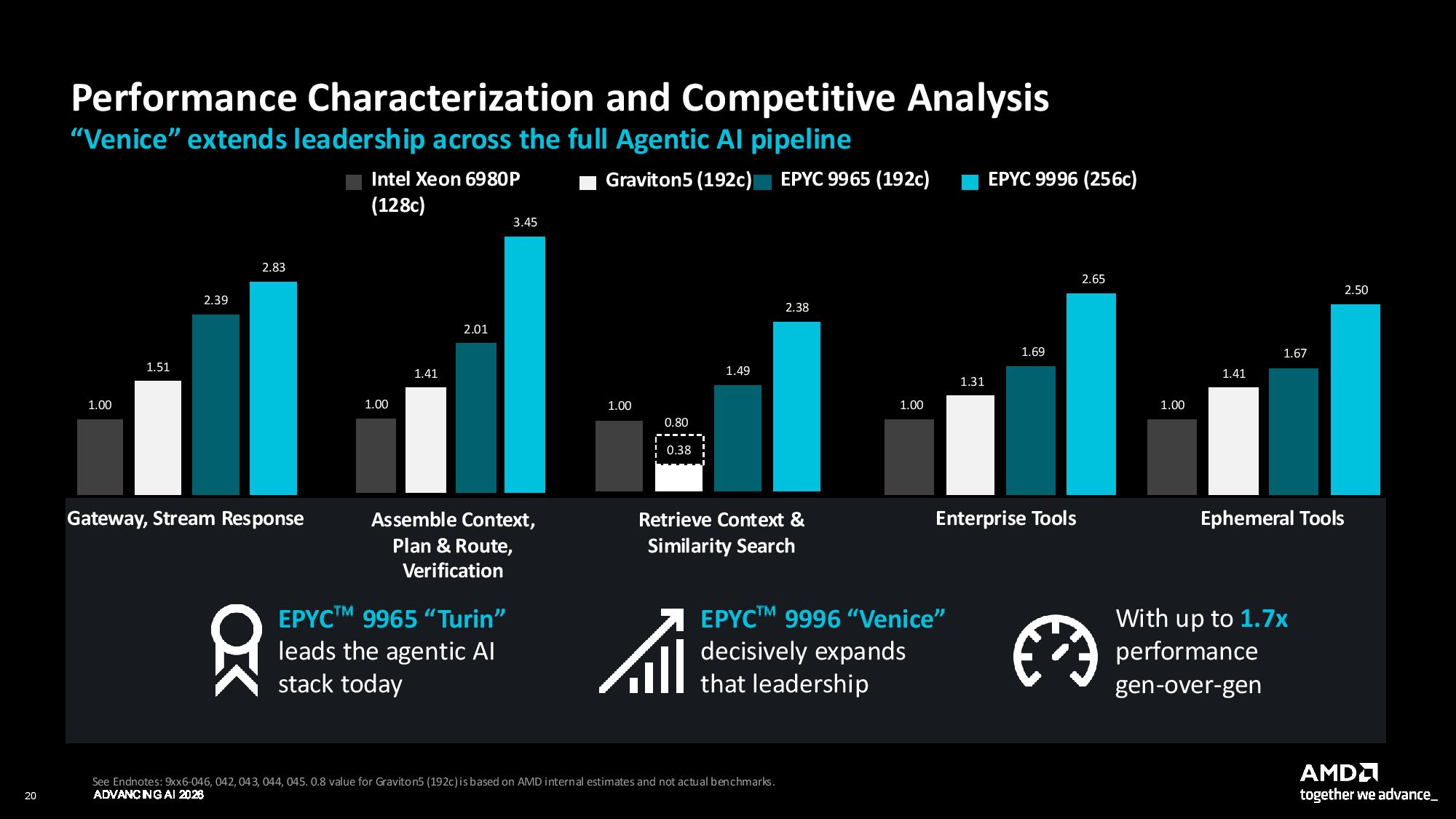
Unlike the extrapolated performance AMD shared a few weeks back, we have some concrete benchmarks for the Epyc 9996 now. AMD has, unsurprisingly, focused the workloads around agentic AI. However, many of the workloads applicable for agentic AI are applicable elsewhere, as well, including high-concurrency networking tasks, code compilation, and media processing.
Note that AMD includes just the Epyc 9965 as a gen-on-gen comparison point in the charts above. This is a “dense” Zen 5 design with 192 cores. Results for the 128-core 9755 are included in the tables below.
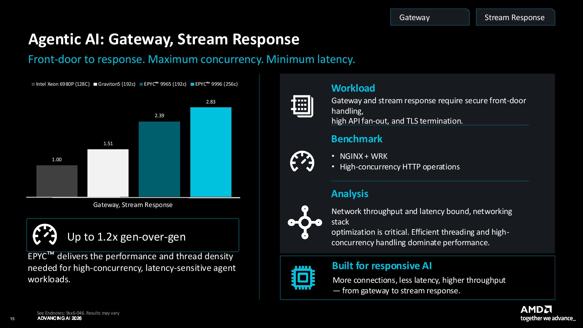
Starting with front-end operations, AMD claims a 1.2x gen-on-gen improvement and a 2.8x improvement compared to Intel Xeon 6980P, with an NGINX web server using the WRK load generator. Unlike most of these competitive performance figures, AMD included the actual numbers for the benchmarks it ran in the footnotes, which you can see in the table below.
Chip
Max Request Per Second
Intel Xeon 6980P
10,162,179
AWS Graviton5
15,331,108
AMD Epyc 9755
17,906,196
AMD Epyc 9965
24,320,476
AMD Epyc 9996
28,789,170
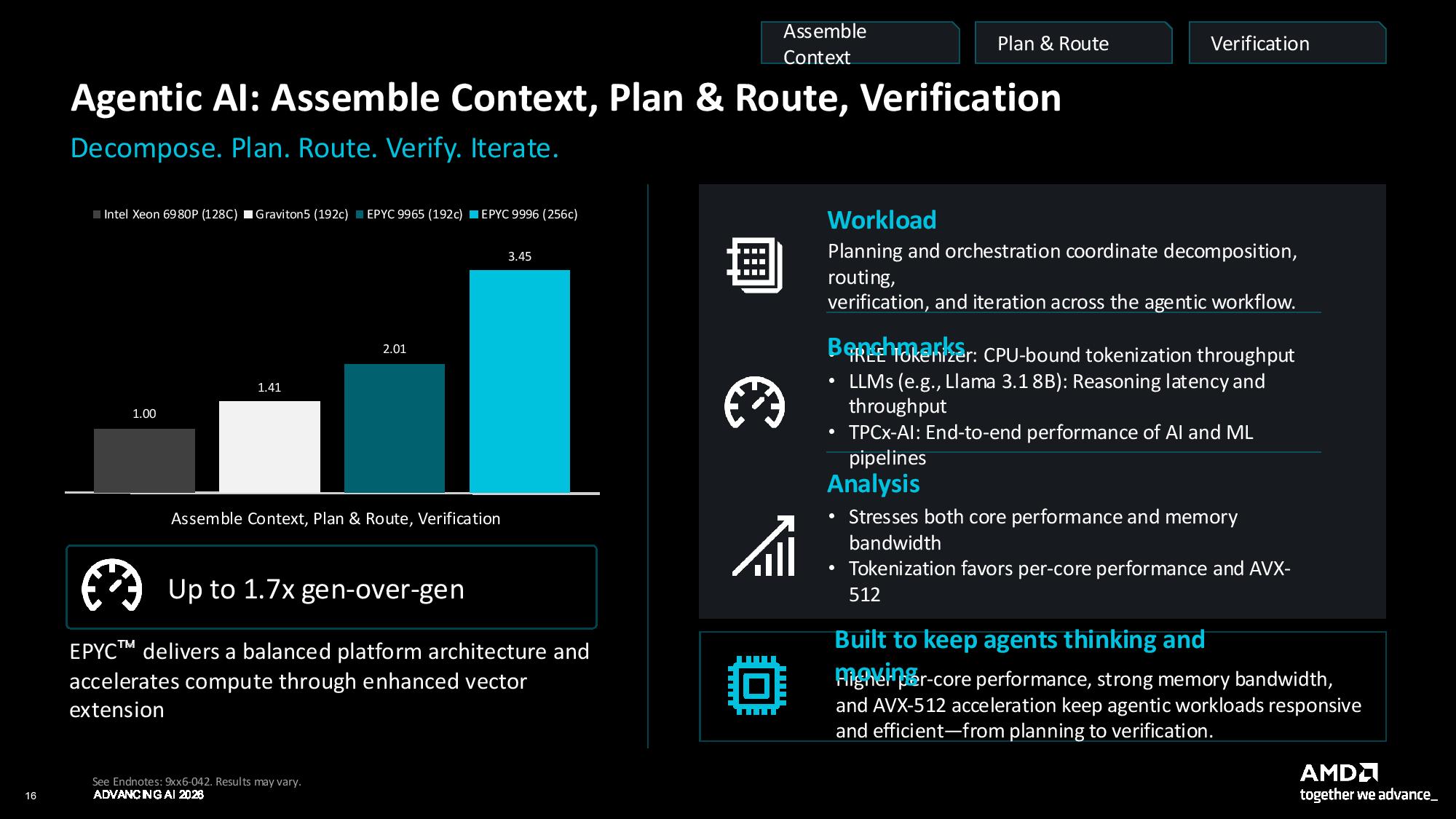
In data-heavy workloads that are common among AI agents, AMD claims a 1.7x improvement over Turn, and a massive 3.4x over the Xeon 6980P. AMD used the TPCx-AI benchmark to gather these results. The primary metric for this test is AI use cases per minute (AIUCpm), for which AMD shared the median result2. If you’re interested in more about the reporting of this benchmark, Dell has published an extensive breakdown.
Chip
AIUCpm
Intel Xeon 6980P
1,750.36
AWS Graviton5
2,444.8
AMD Epyc 9755
2,704.19
AMD Epyc 9965
3,458.79
AMD Epyc 9996
5,982.91
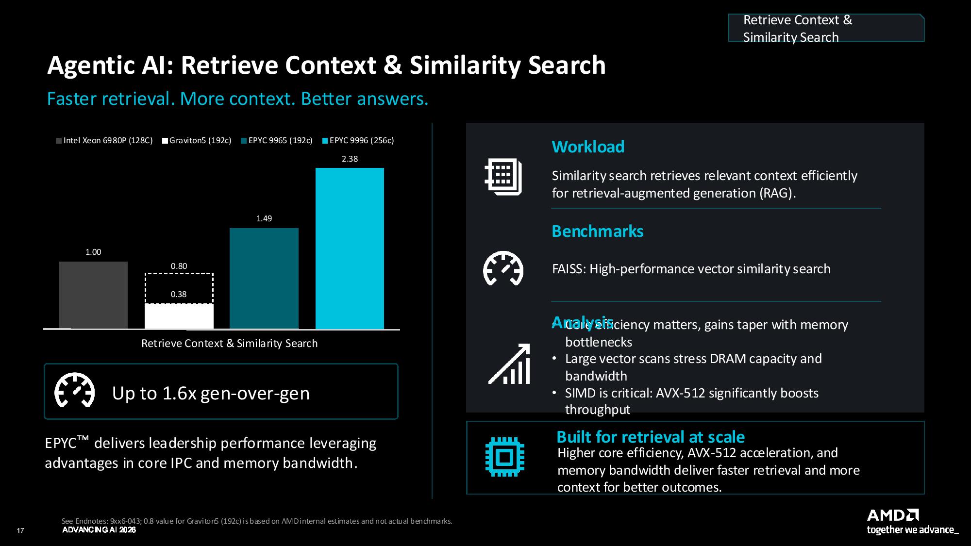
In vectorized workloads, AMD claims a 1.6x gen-on-gen improvement and 2.3x improvement compared to the Xeon 6980P. For this test, AMD used Meta’s open-source FAISS (Facebook AI Similarity Search) library to search for similar vectors in the siftm1 dataset. The metric here is QPS, or queries processed per second, looking at overall query throughput.
Chip
QPS
Intel Xeon 6980P
316,069
AWS Graviton5
119,179
AMD Epyc 9755
369,252
AMD Epyc 9965
472,079
AMD Epyc 9996
751,453
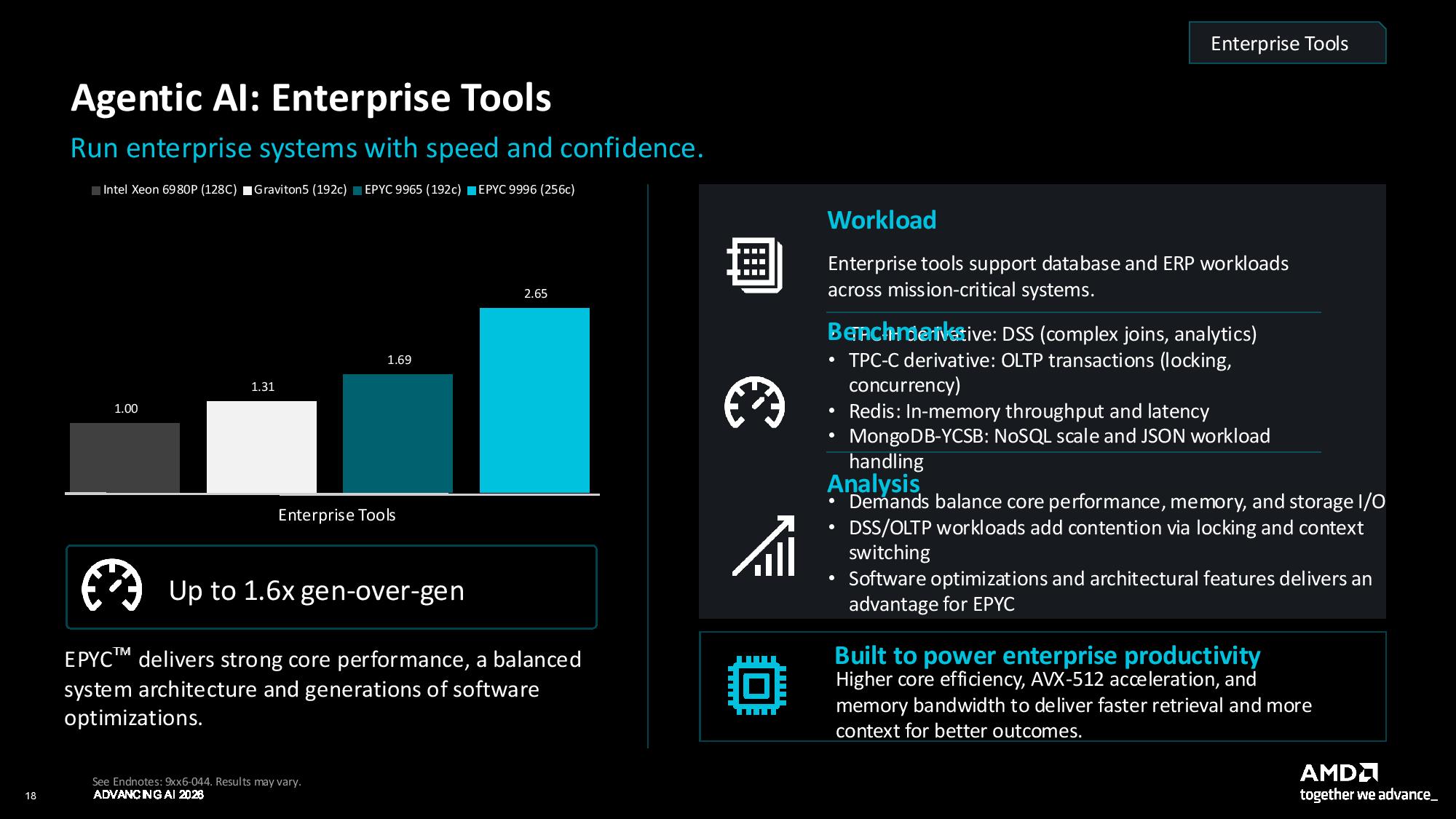
For its “enterprise tools” benchmarks, AMD ran several tests, including TPC-H, TPC-C, and Redis, and it reports the results as “geomean throughput.” We have actual numbers here, but they’re a geomean representing several different tests rather than a single benchmark. Broadly, however, AMD claims a 1.6x gen-on-gen improvement in these workloads, and a 2.6x improvement compared to Intel.
Chip
Geomean throughput
Intel Xeon 6980P
2,284,701
AWS Graviton5
2,982,203
AMD Epyc 9755
2,546,290
AMD Epyc 9965
3,867,149
AMD Epyc 9996
6,054,748
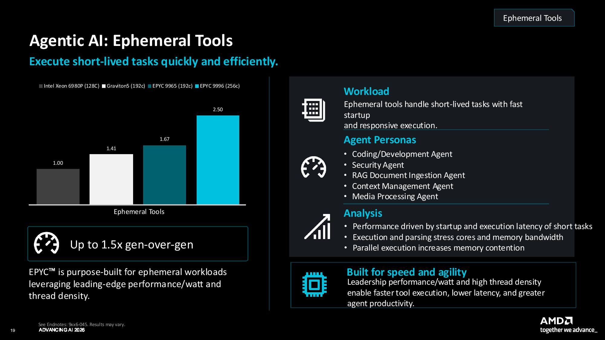
A lot of agentic workloads are applicable outside of agents, but AMD also tested a few agents directly. It replayed five different agent personas across the chips and, once again, gathered a throughput geomean. We don’t have the metrics here, nor for the previous benchmark, so it’s possible there’s an angle of performance that we’re not seeing with the data provided by AMD.
Regardless, the company claims a 1.5x gen-on-gen improvement in this test, and a 2.5x improvement compared to the 6980P.
Chip
Geomean throughput
Intel Xeon 6980P
1.779
AWS Graviton5
2.505
AMD Epyc 9755
2.317
AMD Epyc 9965
2.97
AMD Epyc 9996
4.451
AMD ran these tests earlier in the month. But just a few days ago, Nvidia published its first SPEC CPU 2026 results for Vera. AMD ran some tests of its own using the same compiler for a comparison between Vera and Venice. AMD’s Kuppuswamy says, “everything is apples-to-apples comparison, same compiler.” That’s GNU 15.2, if you’re curious.
(Image credit: AMD)
In throughput, AMD claims a 2.2x improvement in the SPECrate integer suite, compared to Vera using the dense Venice design with 256 Zen 6c cores. More importantly, AMD claims a 1.2x improvement in per-core performance when comparing Vera to a 96-core “High Frequency” Venice chip. AMD says it used Nvidia’s results as the basis for comparison. With both Venice designs, AMD used a 600W TDP.
(Image credit: AMD)
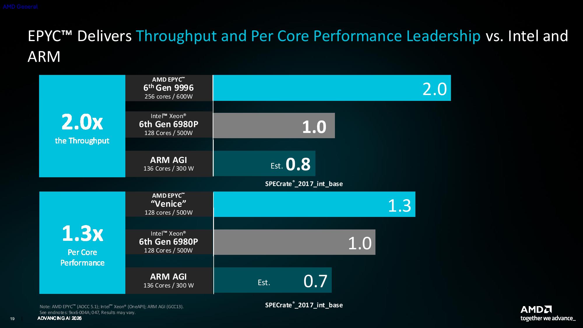
In SPEC CPU 2017 (again using SPECrate with integer workloads), AMD has data comparing Venice to Intel’s 6980P and Arm’s new AGI, showing 2x throughput compared to Intel, and 1.3x per-core performance. Note the core counts here for AMD. SPECrate is a throughput test, and AMD stepping down to a 128-core model suggests that performance will likely drop off as the core count increases.
AMDAMD
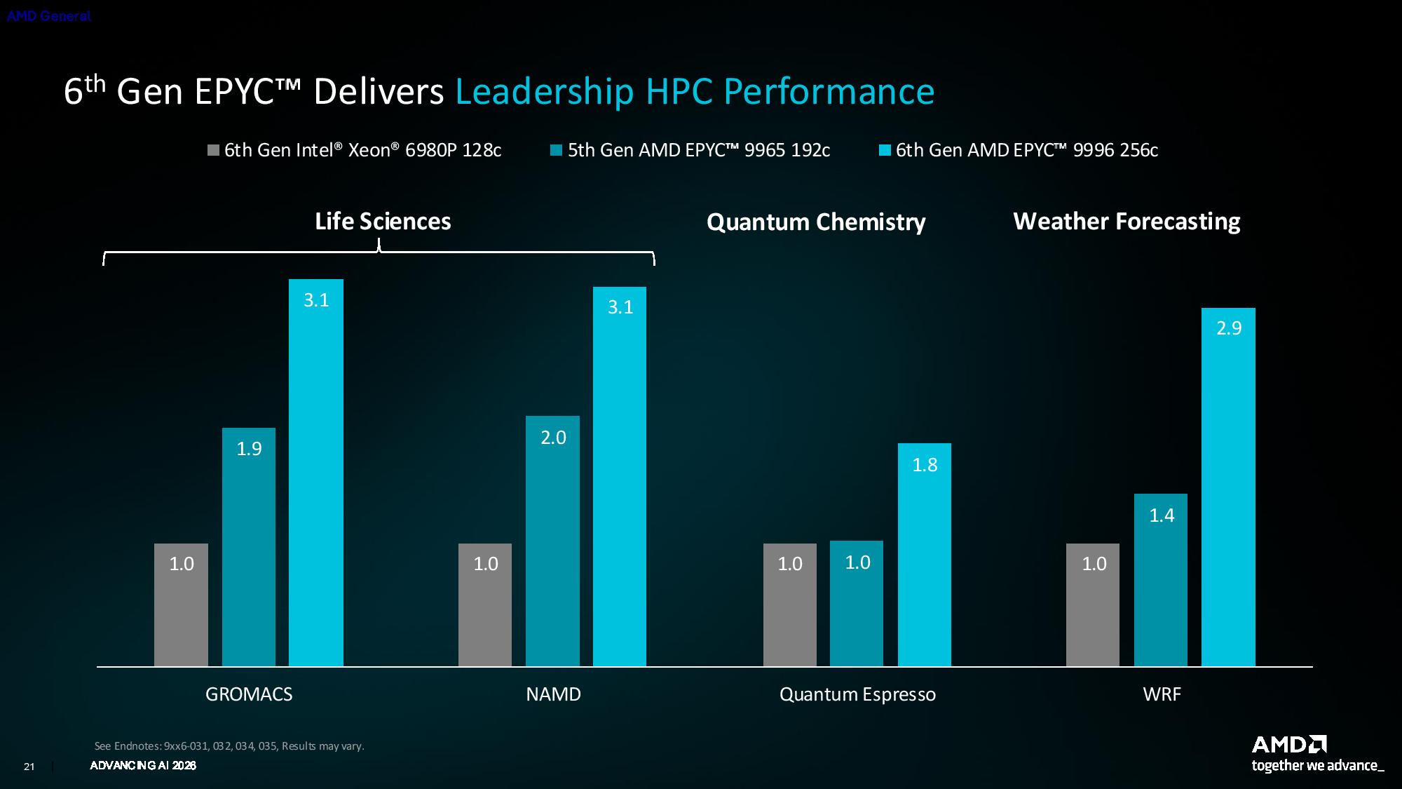
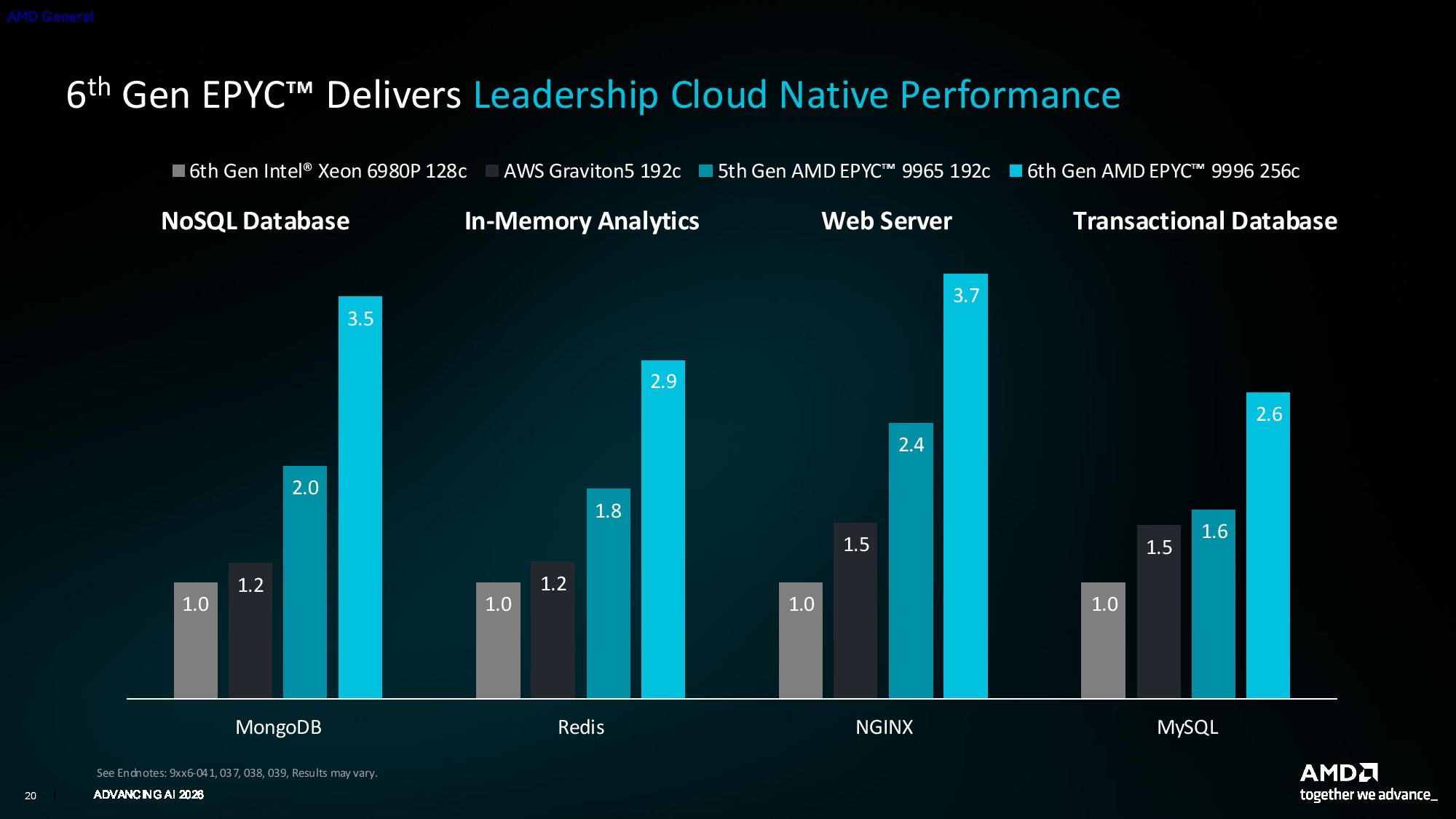
Although AMD wants to focus Venice performance on agentic workloads, it shared a range of what are now being called “legacy” workloads across the cloud and HPC. Some of the results are repeated from the earlier slides, such as Redis and NGINX, but there are some additional data points, including NAMD and SQL. The performance improvements here are large, though not surprising. You can see that across these tests, even Turin beats the competition from Intel and AWS.
AMD’s Venice-X CPU is launching in the second half of 2027, the company revealed Thursday at its Advancing AI event. The CPU is built on the same Zen 6 microarchitecture as Venice SP7, which AMD says is now in production, but it comes with smaller core counts and leverages AMD’s 3D V-Cache to stack an unbelievable 1152 MB of L3 cache on the chip, all while offering 96 cores and clock speeds up to 5.15 GHz.
We’ve previously heard teases of Venice-X, and AMD has released variants of its Epyc chips like this in the past, such as Milan-X and Genoa-X. But we never saw Turin-X, and we haven’t gotten any concrete details about Venice-X up to this point. Now, we have a peek into what Venice-X will offer, which looks similar to Genoa-X in some regards.
AMD is sticking with 96 cores with Venice-X, as well as 1152 MB of stacked L3 cache. There are a few major differences compared to Genoa-X, however. First, AMD says clocks are much higher here, claiming Venice-X tops out at 5.15 GHz (the 96-core Epyc 9684X clocks up to 3.7 GHz). Venice-X also comes with the memory improvements available in most of the chips in the range.
It supports 16-channel memory, either with standard DDR5 RDIMMs at up to 8,000 MT/s or with new MRDIMMs 12,800 MT/s, offering up to 1.6 TB/s of aggregate memory bandwidth. The memory system in Venice broadly is a massive increase over Turin, nearly tripling the aggregate bandwidth, mainly on the back of speeds enabled by MRDIMMs.
Venice-X is one of four variations of AMD’s Zen 6 lineup for data centers, mainly targeting HPC workloads, with its massive L3 cache and relatively high clock speeds. Venice-X uses the same SP7 socket as the main Venice range. Other variations of Zen 6 offerings, including Verano, will use the SP8 socket instead.
AMD’s standard Venice chips support up to 1024 MB of L3 cache on their own, nearly triple that of its previous flagship offering. That cache is split among 256 cores, however. Venice-X doesn’t come with much more cache overall, but that cache is serving far fewer, more powerful cores, which should be useful in HPC workloads.
AMD didn’t disclose any other details about Venice-X, nor any performance projections. Given that it’s set to launch in the second half of 2027, we’re still a ways out from that.
Intel and AMD are signing longer-term purchase commitments with Chinese server customers for data center processors, according to a new Reutersreport that cites two people familiar with the talks. Prices for some server CPU products in China have climbed more than 40% since the start of the year and are still rising by over 10% month-on-month in some cases, one of the people said. Most of the agreements guarantee purchase volumes for about a year without fixing prices, and neither company responded to the publication's requests for comment.
Some customers have discussed commitments running two years or longer, one of the people told Reuters, with the deals covering unit volumes only, which leaves Chinese cloud providers and internet companies fully exposed to a market that has already added 40% to some CPU prices in under seven months. Memory makers struck similar long-term agreements with hyperscalers over the past year as AI demand consumed DRAM and NAND output, but those contracts typically trade a volume commitment for some pricing visibility. Buyers here get neither price protection nor, based on current lead times, fast delivery, but they do get a place in the queue.
Intel said in March that it was pursuing long-term agreements with potential customers as server CPU demand spiked, with CEO Lip-Bu Tan telling analysts on the company's April earnings call that demand "continues to run ahead of supply," singling out Xeon server parts. Tan also cited a multi-year supply deal with Google among several long-term contracts signed in the first quarter, so the model now spans U.S. hyperscalers and Chinese channel buyers alike.
Reuters first reported in February that Intel had warned Chinese customers of lead times stretching to six months on some server CPUs, with AMD quoting eight to 10 weeks. By late March, server makers told Nikkei Asia that average CPU lead times had blown out from one to two weeks to eight to 12 weeks and beyond. Intel CFO David Zinsner put a value on that in April, telling investors that unmet Xeon demand "starts with a B," and the company later confirmed price hikes on select consumer and server CPUs.
Agentic AI workloads are driving much of the demand, as inference and orchestration tasks pull server CPU-to-GPU ratios back toward parity. AMD, which is due to report earnings in early August, has raised its server CPU market forecast to more than $120 billion by 2030, based on the same trend.
Intel will report its second-quarter results later today, where the shortage and the durability of these commitments are likely to come up. Chinese buyers remain cut off from the most advanced AI accelerators under U.S. export controls, but Xeon and EPYC server CPUs carry no such restrictions, making them one of the few U.S.-made AI infrastructure components China can still purchase freely, if it can get them.
Nvidia’s Vera CPU is its first bid to become a key player in the data center CPU market. Although Grace has seen some success (most notably with Grace standalone deployments at Meta), Vera is Nvidia’s first CPU with a custom core design. It’s arriving at an ideal time, as well, with the server CPU market exploding in the last few months on the back of agentic AI demand.
Vera isn’t a chip built to chip away at the market share of AMD and Intel in the cloud. It’s built to grab market share in an expanding market, as hyperscalers look to widen AI infrastructure beyond legacy clouds. As such, it’s designed in a much different way than Nvidia’s x86 competitors, and it even holds some unique architectural design points compared to the swath of Arm-based designs.
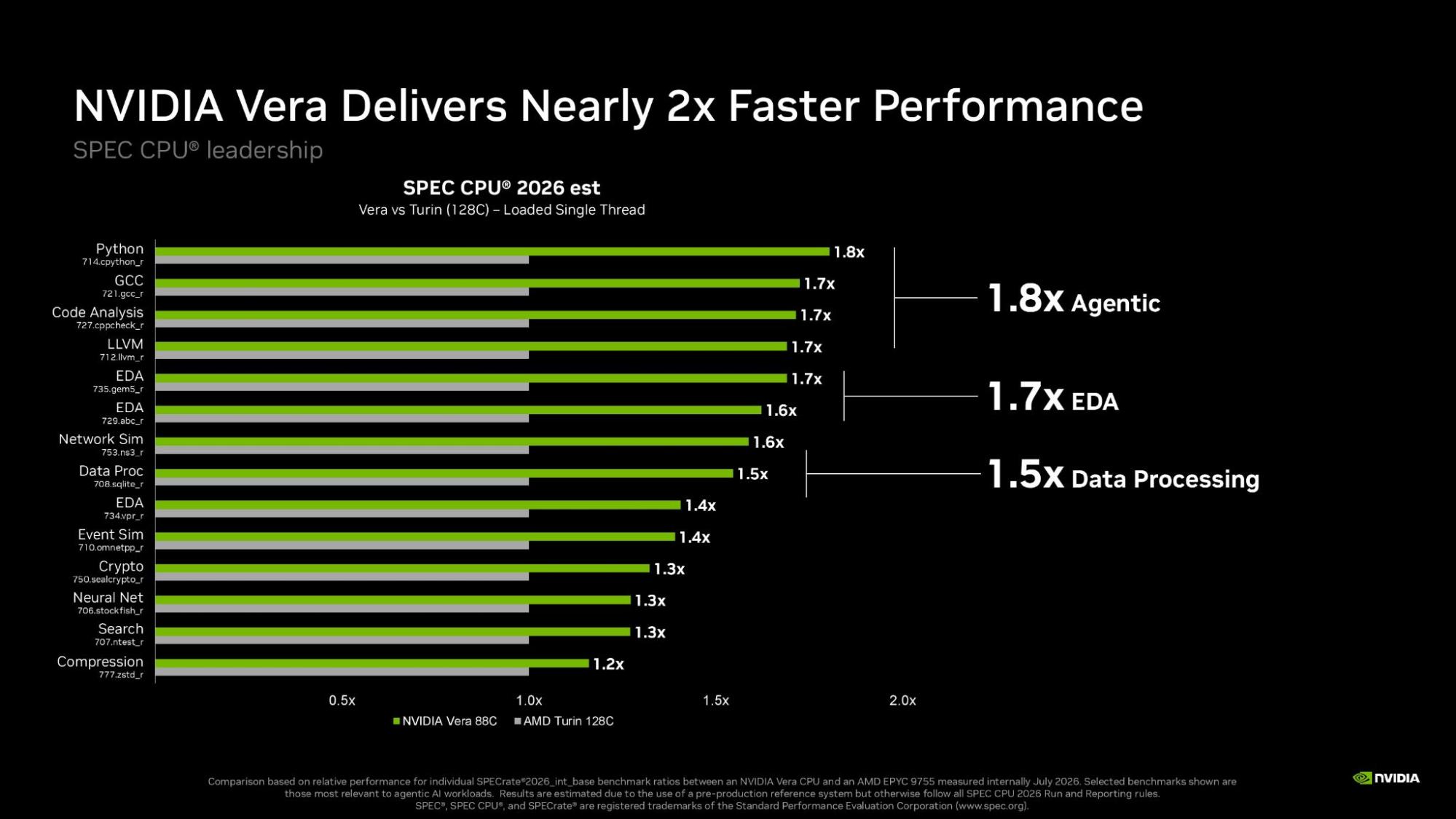
Nvidia has slowly revealed more details about Vera as it ramps into general availability, which is on track for the back half of this year. Now, we have a full picture of the chip. Nvidia shared its Vera white paper, along with unofficial SPEC CPU 2026 results comparing Vera to AMD’s Turin-based Epyc 9755.
We’re going to break down the white paper here, including all of the details about the Olympus core and a look at the benchmarks Nvidia ran. At the end of this piece, we’ll also take a brief look at the larger context of Vera and how it fits into Nvidia’s wider AI ecosystem compared to standalone deployments.
But plenty of ink has been spilled about Vera’s technical capabilities and Nvidia’s next-gen AI infrastructure vision. Let’s start with the important thing: the benchmarks.
Nvidia Vera CPU benchmarks
We’ve seen Vera in action before, though only through a series of selected benchmarks ran at Nvidia HQ by Phoronix. In the Vera white paper, Nvidia shared benchmarks for SPEC CPU 2026, specifically the integer suite from SPECrate, against AMD’s Epyc 9755, with both chips running in a dual-socket configuration. Before getting into the results, there are some important notes about how SPEC runs work, and the reporting criteria for them.
Nvidia’s run here isn’t official, as Vera was tested in a reference system due to the fact that it’s not broadly available yet. It’s ramping for general availability in the second half of the year. Due to that, Nvidia is unable to report its results. That’s why you see “estimated” in some of the charts below. Nvidia ran SPEC CPU 2026; it’s not extrapolating expected performance like we’ve seen from AMD so far with its upcoming Venice chips.
SPEC CPU 2026 is split into four suites, but Nvidia tested the SPECrate integer suite, which is focused on system throughput with integer-based workloads. The “rate” result is looking at how much work is completed within a certain amount of time. Here, each thread in the system has a copy of the workload. The score is how much time it takes for those workloads to complete, regardless of thread count, naturally giving chips with more cores an advantage.
If you want more detail on the benchmarks included in the suite, make sure to read our original coverage of SPEC CPU 2026. Here are the overall results:
Test
Run Time
Rate
706.stockfish_r
324
1370
707.ntest_r
251
830
708.sqlite_r
250
744
710.omnetpp_r
203
842
714.cpython_r
136
1240
721.gcc_r
296
817
723.llvm_r
196
909
727.cppcheck_r
142
890
729.abc_r
196
823
734.vpr_r
199
815
735.gem5_r
131
1300
750.sealcrypto_r
231
816
753.ns3_r
129
1670
777.zstd_r
469
483
Overall base score
925
Nvidia didn’t share the exact results for the 9755 it tested, short of the overall score of 898. Taking that overall score into account, Vera is 3% ahead of the 9755. It’s worth noting that Vera is ahead here despite a large thread disadvantage. An overall score of 898 for a dual-socket Epyc 9755 system isn’t unreasonable compared to publicly-submitted SPEC CPU 2026 runs, though higher results have been published. SPEC CPU ships as source code, which the tester must compile with their compiler of choice, and that can heavily influence results (particularly with vendor-specific compilers). Nvidia used GNU 15.2 with both systems.
(Image credit: Nvidia)
Above, you can see Vera’s results stacked up against the 9755, but these aren’t comparing the numbers directly. Nvidia has normalized the per-core performance, which isn’t how SPECrate results are normally shared. According to the overall numbers, Vera is still completing more work within the same amount of time, despite a thread disadvantage, but the margins aren’t in the range of a 70% or 80% advantage as the above chart suggests.
We asked Nvidia about the results given that they're obfuscated by comparison; we could not reverse-engineer the Epyc 9755's scores with the information Nvidia has provided. Here's the response it gave: "Per-core performance under a fully loaded socket is important because agentic AI and RL run many sandboxes concurrently, while each agent step remains sequential and latency-sensitive. It measures how much performance each core sustains amid contention for shared power, memory, cache, and fabric. We therefore normalize by physical core, with SMT enabled on both systems."
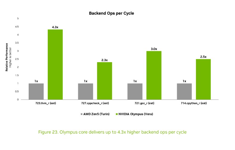
The “agentic” workloads Nvidia has highlighted here are code compilation and interpretation workloads, which is something an agent is often doing, querying repos for dependencies and building source code. Below are data science workloads (or Exploratory Data Analysis), and below that are data processing workloads like SQLite database management. The results here align with Nvidia’s overall messaging of Vera, that it’s highly competent at data-rich, backend operations.
Although Nvidia is sharing per-thread results, it argues that SPECrate is still the correct benchmark to run. The per-thread results here are in the context of a fully-loaded socket. Here’s the justification from the white paper: “This metric is non-trivial for agentic AI and RL systems, where many sandboxes, tools, and environments run concurrently rather than as isolated single-thread tests. Fully loaded per-core performance captures how well each core sustains throughput while sharing socket-level power, memory bandwidth, cache, and fabric resources.”
NvidiaNvidiaNvidiaNvidiaNvidia
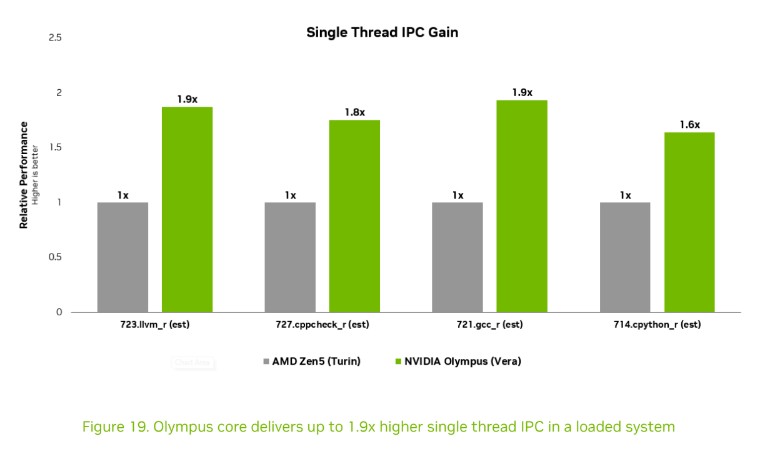
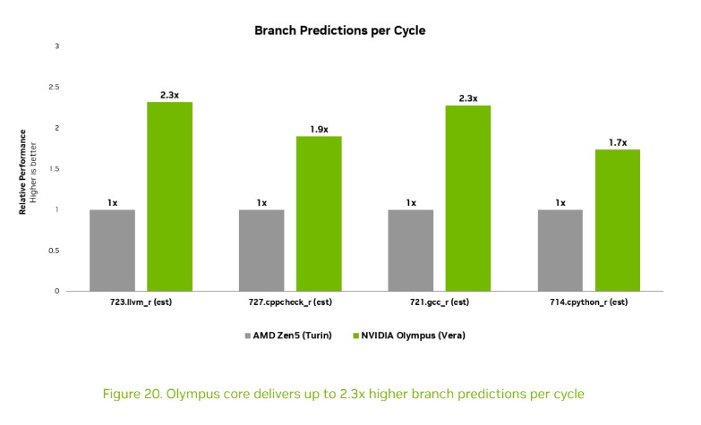
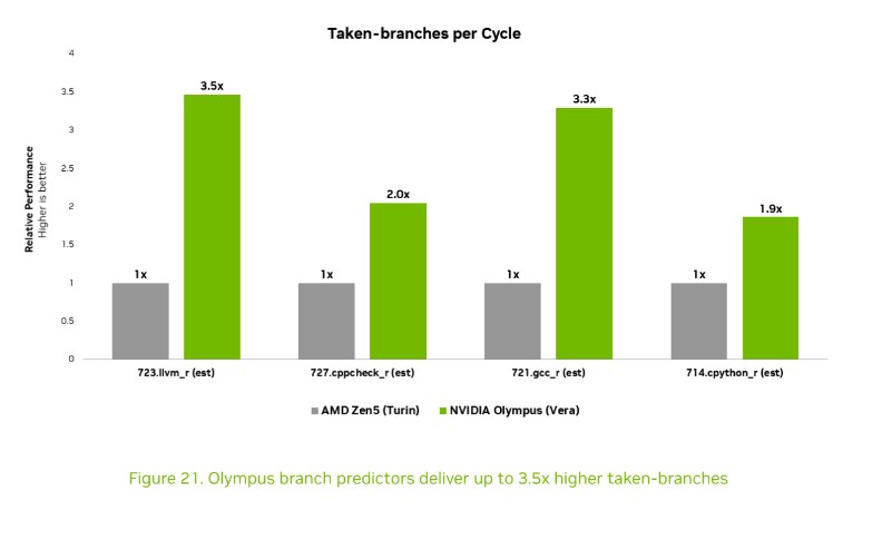
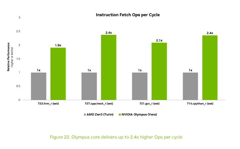
In addition to running the workloads, Nvidia analyzed the code execution for architectural benchmarks, which you can see in the gallery above. Nvidia claims an overall IPC gain of up to 1.9x compared to Turin, up to 2.3x more branch predictions and 3.5x taken branches per cycle, and up to 2.4x higher instruction fetch operations per cycle.
NvidiaNvidia
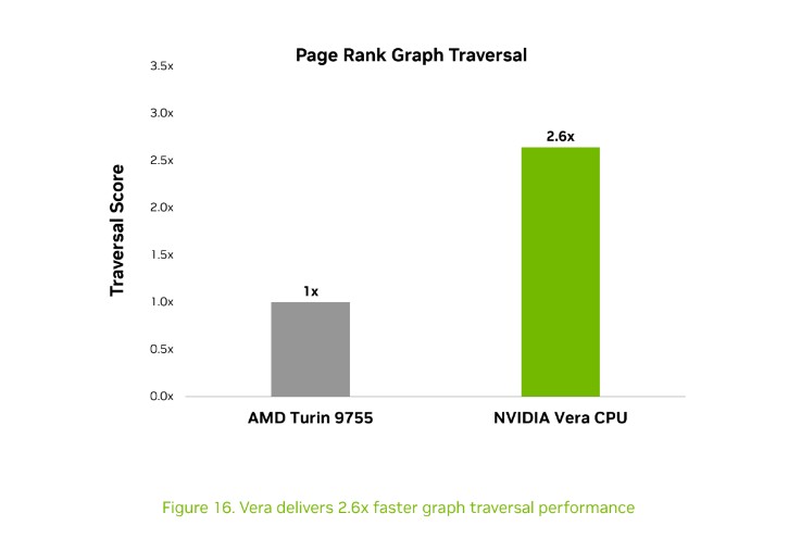
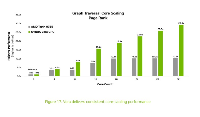
Outside of SPEC, Nvidia shared a few benchmarks highlighting the capabilities of the Olympus core. First up is PageRank, an algorithm developed by Google to originally rank web pages, which highlights Olympus’ prefetch engine. Nvidia scaled this workload to higher core counts, showing Vera maintaining much of its single-core performance up to 32 cores, while the Turin chip hits a wall around 20 cores.
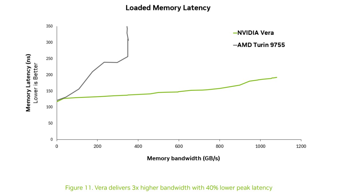
In addition to the above results, Nvidia shared some tests of the Vera memory system compared to Turin. These microbenchmarks are good for validating Nvidia’s specifications, but they’re looking at architectural performance, not application performance. An architectural advantage translates into a performance advantage, but not always in a linear, expected fashion.
Nvidia used internally-developed tools for the memory tests, though they're available on GitHub for anyone to run.
(Image credit: Nvidia)
First is loaded memory latency, stressing the memory subsystem as bandwidth usage increases. Vera has much higher bandwidth overall, but you can see the Turin chip hit a latency wall below its maximum, which Nvidia attributes to Non-Uniform Memory Access (NUMA) domain traversal and CCD-to-CCD latency.
(Image credit: Nvidia)
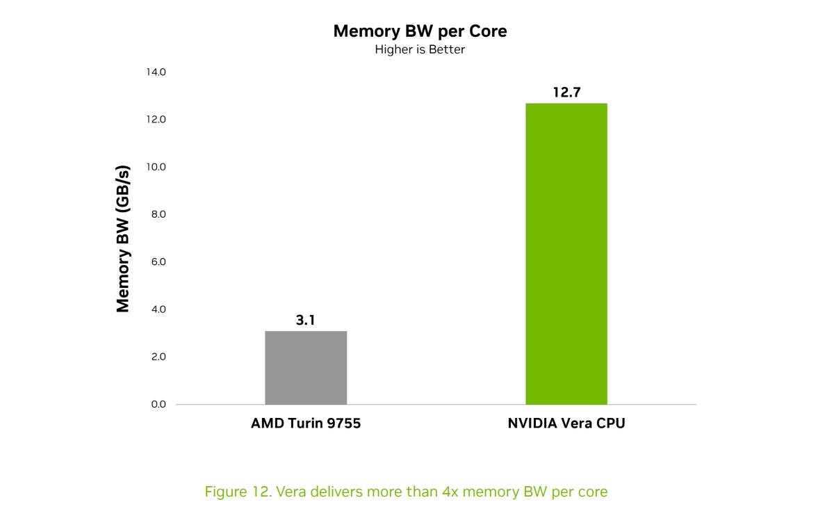
Looking at per-core bandwidth, Nvidia claims Vera provides more than four times the bandwidth of AMD’s 9755. The suggestion here is that “real-world” per-core bandwidth is even better than Nvidia’s specs lead on (or perhaps worse than AMD’s).
(Image credit: Nvidia)
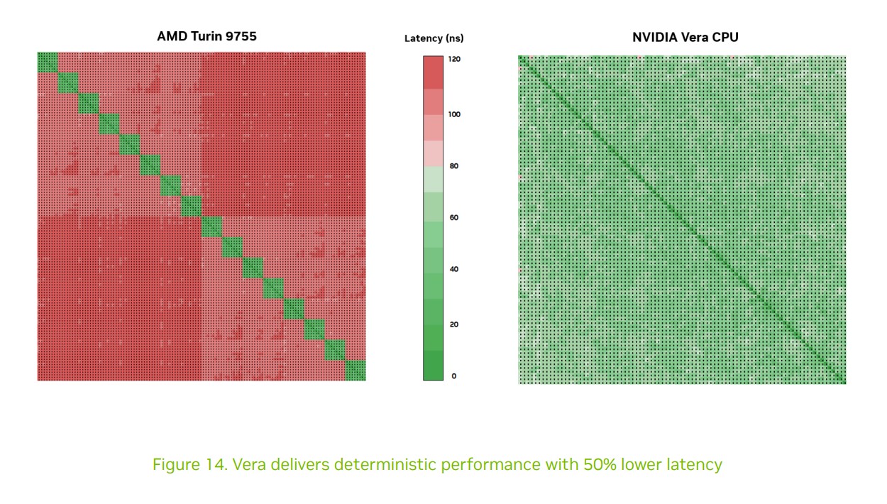
Maybe the most consequential of these tests is the one you can see above, looking at core-to-core latency. It’s no secret that crossing the CCD on AMD’s chiplet-based architecture incurs a big latency penalty. You can see that in action even in our Ryzen 9 9950X3D2 review, and the penalties compound as you scale up the number of CCDs.
In fairness to AMD here, chiplet-based designs aren’t built for this type of cross-CCD traversal, preferring to keep workloads localized and optimizing for core density. Vera’s design goal is clearly to keep latencies consistent across the entire die and sacrificing core density in the process. Nvidia’s Ian Buck told us that this design trade-off “will come at the cost of the legacy workload,” when we recently visited Nvidia HQ.
That’s important context. Nvidia isn’t gunning to steal existing market share from AMD and Intel as much as it’s trying to grab market share in an expanding market before AMD and Intel can. Some financial institutions (including Morgan Stanley and Bank of America) suggest the server CPU market could double in size (or grow even larger) by 2030. That context is important because there will be a continuing demand for CPUs that can handle workloads Vera is not optimized for, and it’ll be interesting to see how AMD and Intel tackle that dynamic with future products, trying to keep a legacy base of customers while pushing ahead into the expanded market.
Nvidia clearly has a vision of how that expanded market looks, and to that end, hasn’t shared SPEC CPU floating point results. Presumably, this is due to the fact that SPEC’s vectorized suite is focused primarily on HPC workloads, whereas Nvidia focused on what it believes are critical agentic workloads that are integer-based. Vera has a vector engine complete with SVE, but that doesn’t seem like Nvidia’s focus.
In an end-to-end Nvidia system, those vectorized workloads would be offloaded to a Rubin GPU. Still, we don’t have any vector results for Vera yet. Up to this point, we’ve only seen integer results, which is strange given the memory system at play in Vera.
(Image credit: Nvidia)
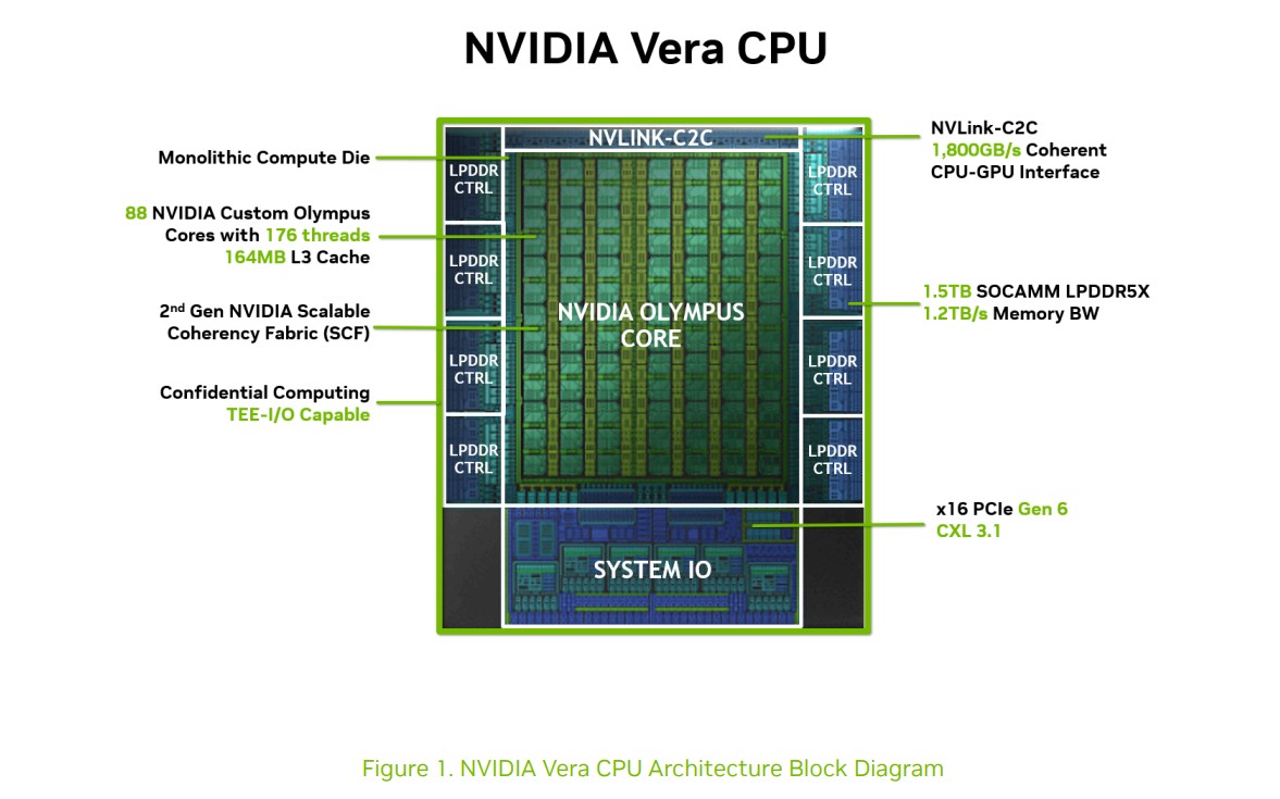
Vera is Nvidia’s first CPU with a core design created in-house, which is the Olympus core. It’s built on Arm v9.2-A, but the design was created by Nvidia, unlike Grace, which leveraged a stock Arm design. Each Vera CPU has 88 Olympus cores on a monolithic die, breaking from the chiplet-based designs available from Nvidia’s x86 competitors.
Nvidia says Vera comes with a 1.5x increase in instructions per cycle (IPC) throughput compared to Grace, and 50% higher performance compared to x86 competitors (it seems that number is per-thread performance with a fully-loaded socket). Nvidia has a single 88-core design with Vera that supports spatial multithreading for 176 threads.
Cores / Threads
88 / 176
L2 cache
2 MB per core
L3 cache
164 MB per CPU
Memory
Up to 1.5 TB SOCAMM2 LPPDDR5X
Memory speed
Up to 9600 MT/s
Memory bandwidth
Up to 1.2 TB/s (aggregate), 14 GB/s (per core)
PCIe
88 PCIe 6.4 lanes (CPU only), 96 PCIe 6.4 lanes (Vera Rubin), bifurcation down to x2, CXL 3.1
Configurable TDP
250W - 450W
The CPU has a configurable TDP range of 250W to 450W. It uses a SOCAMM2 LPDDR5X memory system with capacity of up to 1.5 TB and speeds up to 9600 MT/s, and comes with 164 MB of L3 cache and 2 MB of L2 per core. Vera includes significantly less L3 than Intel’s highest-specced Xeon 6 and AMD’s Zen 5 chips. It actually has more L2 than L3 overall. This, presumably, is due to Nvidia’s fabric, which distributes the L3 in a mesh across the monolithic die.
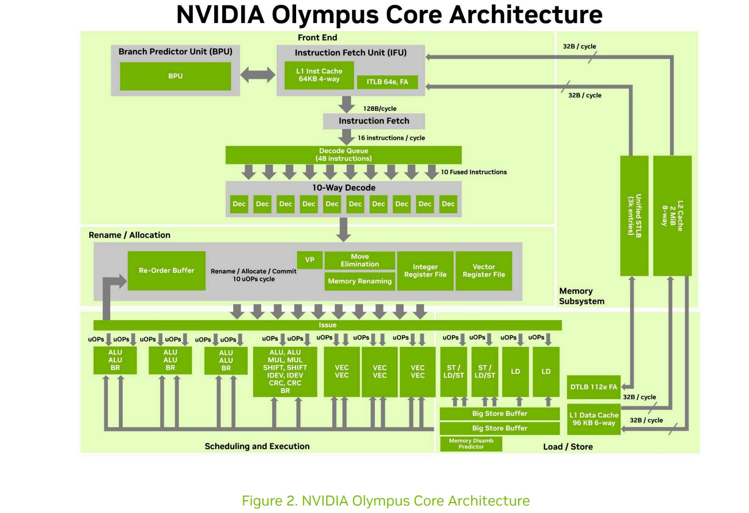
Below, you can see a layout of the Olympus microarchitecture. Nvidia has disclosed some of the highlights of the architecture previously, such as the 10-wide instruction decode and neural branch predictor, but we now have a full view of the architecture courtesy of Nvidia’s Vera white paper.
(Image credit: Nvidia)
The front end starts with Nvidia’s neural branch predictor that can run two branches per cycle “with zero penalties,” according to Nvidia. Research on neural branch prediction dates back to the late 90s, but Nvidia says it has a “novel” neural branch predictor, perhaps building on previous research such as BranchNet.
The BPU feeds into the Instruction Fetch Unit, which holds 64 KB of L1 instruction cache, and loads into a decode queue that supports 48 instructions (we’ll go into the memory/cache layout later). At the last stage of the front end is that 10-wide decode, feeding more instructions into the execution engine per cycle than the 8-wide decode in AMD’s Zen 5 microarchitecture.
Past the front end, the mid-core rename / allocation engine is built to keep instructions moving while waiting on dependencies. In addition to renaming and allocation, instructions work through value prediction, which can speculatively execute the instruction, and memory renaming, where the instruction can move forward while a load is happening if the data relationship can be determined.
(Image credit: Nvidia)
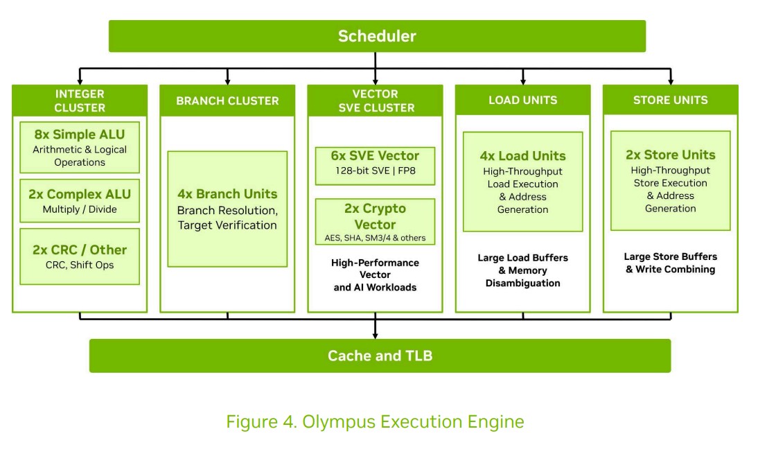
Inside the execution engine, Nvidia includes eight simple Arithmetic Logic Units (ALUs), two complex ALUs, and four branch units for resolution. For SIMD instructions, the execution engine includes a vector cluster for Arm’s Scalable Vector Extension (SVE), including six vector units that support 128-bit SVE instructions at FP8 precision, along with two crypto-enabled vector units that can handle AES, SHA, and SM3, among other prominent algorithms. Keeping data moving through the engine are four load units and two store units.
(Image credit: Nvidia)
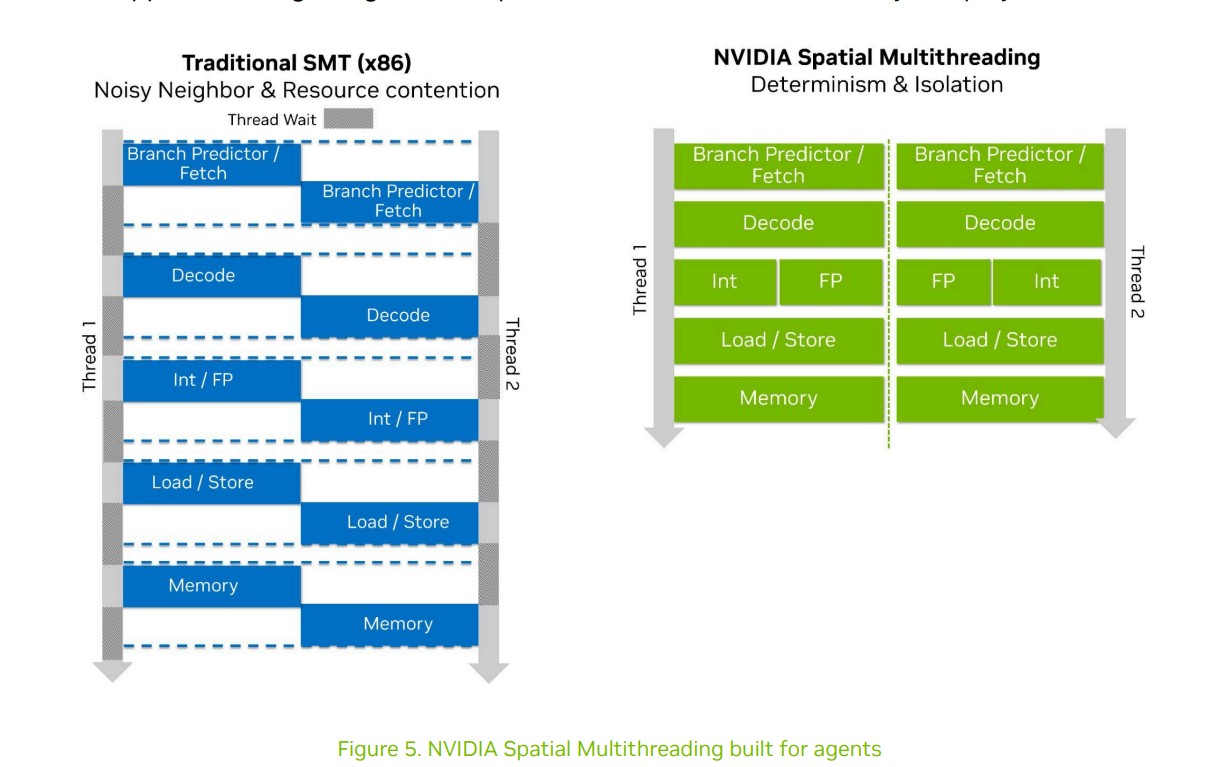
The cores support spatial multithreading, giving a Vera CPU with 88 cores access to 176 threads. Traditional SMT time-slices execution, giving both threads access to all of the core resources and sharing them as instructions execute in parallel. With spatial multithreading, each thread of an Olympus core has access to dedicated resources, allowing one of the threads to execute with high-throughput while the other thread handles simple tasks, or to operate as two independent execution environments.
The execution resources are partitioned, explaining the wide decode front end. It’s not clear, however, if the SMT implementation can also opportunistically grab resources, particularly in the scenario Nvidia describes where one of the threads is maximizing throughput while the other handles smaller tasks.
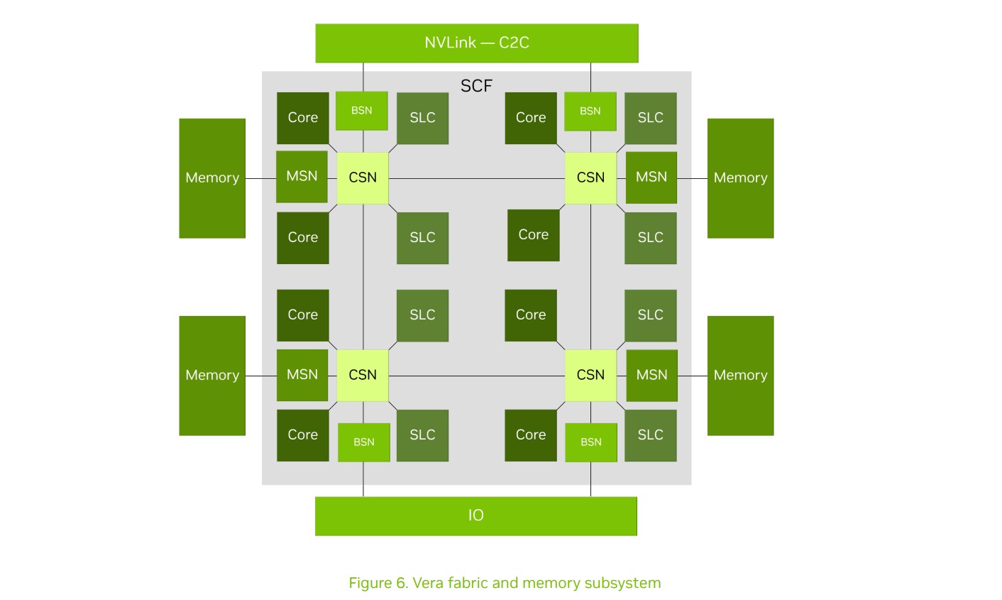
There’s a lot going on in Vera between the 10-wide decode, neural branch predictor, and spatial multithreading, but perhaps the most significant architectural design point is Nvidia’s second-generation Scalable Coherency Fabric (SCF). It underpins Nvidia’s approach of using a monolithic die as opposed to a chiplet-based design, distributing last level cache in a mesh across the die and avoiding the cross-CCD latency penalty with localized L3.
(Image credit: Nvidia)
The mesh distributes data through a series of Coherency Switch Nodes (CSNs) that serve as routing points between cores and the 164 MB of distributed L3. These routing points further connect the cores and L3 to the memory system, I/O, and NVLink C2C for cache-coherent communication between chips. Nvidia’s benchmarks comparing Vera to AMD’s Epyc 9755 show that AMD can achieve slightly lower core-to-core latencies within a cluster, but Vera maintains significantly better core-to-core latency across the die, as expected.
Nvidia says SCF inside Vera has 3.4 TB/s of bandwidth, enabling faster core-to-core communication, especially when traversing the die. However, Vera also supports Memory System Resource Partitioning and Monitoring (MPAM), allowing portions of L3 to be partitioned in multi-tenant environments.
Vera uses SOCAMM2 LPDDR5X, which is a relatively new advancement that Nvidia’s competitors haven’t had the chance to benefit from. With the use of SOCAMM2, LPDDR5X provides similar modularity and capacity as traditional RDIMMs, but at significantly lower power draw.
The memory can run at up to 9600 MT/s, with aggregate bandwidth of 1.2 TB/s and per-core bandwidth of 14 GB/s, doubling the bandwidth of Grace. The Vera board supports eight SOCAMM2, offering capacity ranging from 256 GB to 1.5 TB. Nvidia claims a “fully populated” memory subsystem consumes between 30W and 40W depending on capacity.
For I/O, Vera supports PCIe 6.4 with 88 lanes per CPU and bifurcation support down to x2. It also supports CXL 3.1.
Unlike Grace, Vera includes Arm’s Confidential Computing Architecture (CCA) and Realm Management Extension (RME), including Device Assignment and Coherent Device Assignment, offering a boon to multi-tenant environments where VM isolation is key. Nvidia also implements TDISP for coherent devices, allowing for encrypted communication between GPUs and PCIe devices.
(Image credit: Nvidia)
Nvidia is already sampling Vera as a standalone chip to partners, and it says it will continue to do so, but the vision is an end-to-end solution built on Nvidia’s CPUs, GPUs, switches, NICs, and even rack specifications. Nvidia doesn’t make all of these individually, at least not at scale — just like with desktop graphics cards, Nvidia provides its MGX reference design, which customers can purchase, but partners also offer their own racks, some built solely to Nvidia’s specifications and others with more speciality.
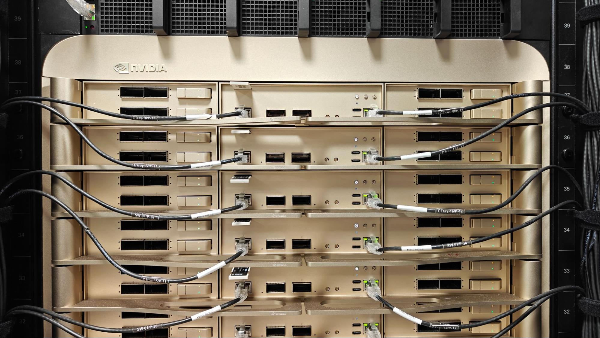
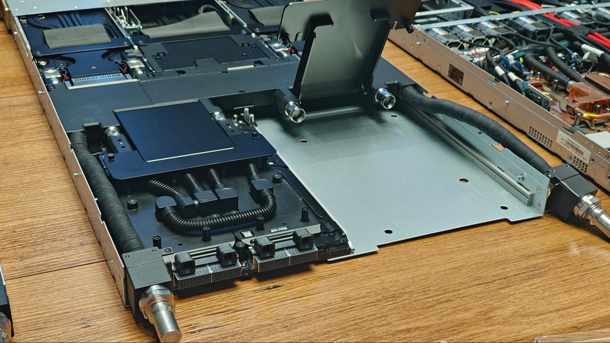
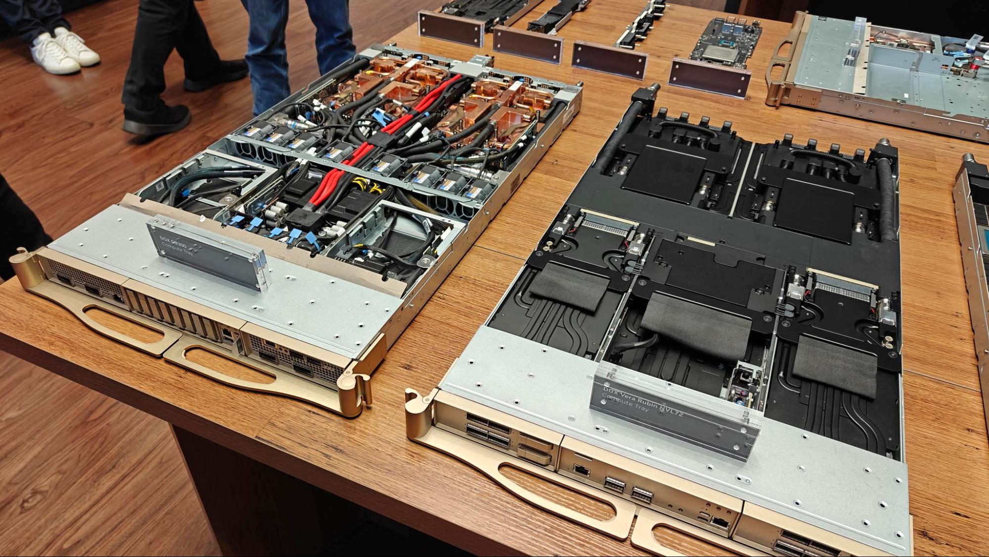
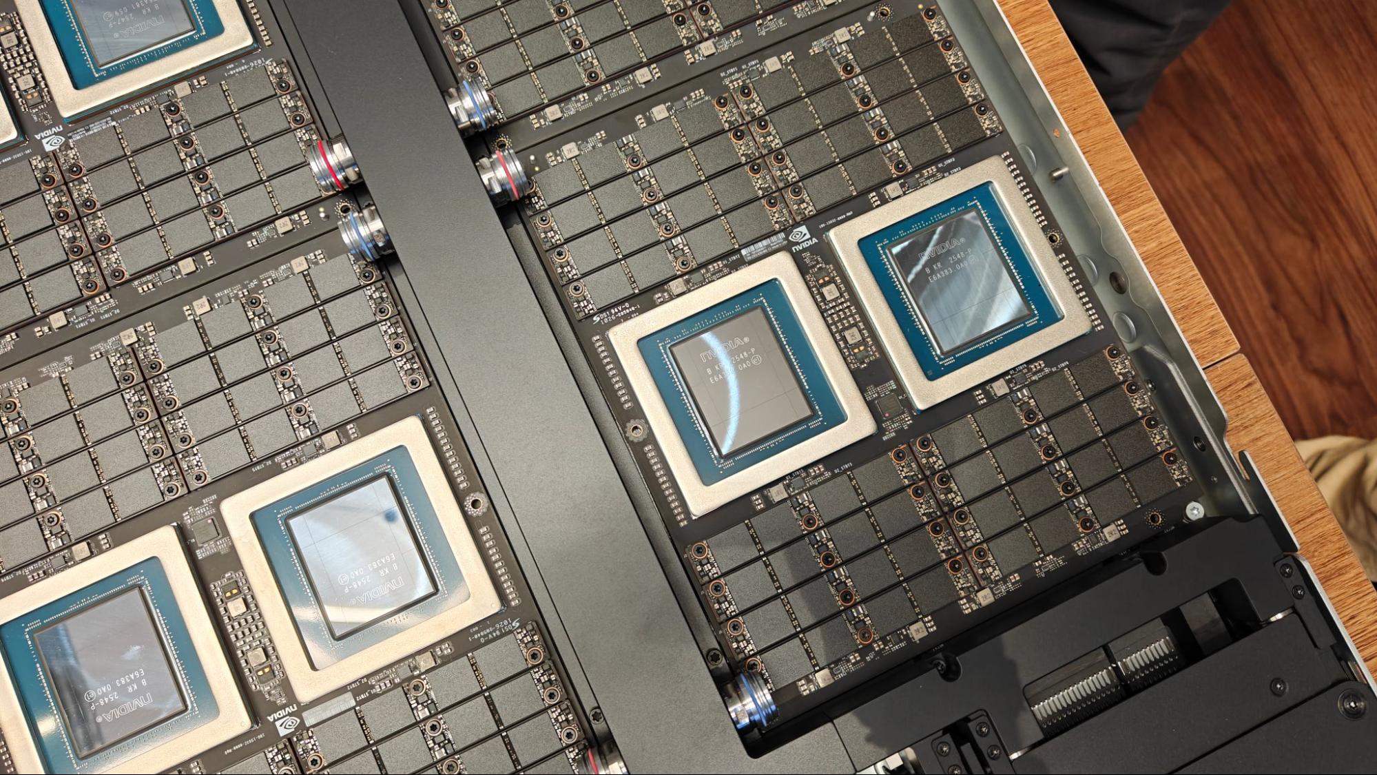
Each tray comes with two Vera Rubin superchips, each of which contain a single Vera CPU to two Rubin GPUs, giving you two CPUs and four GPUs per tray. At the front, Nvidia partitions off three spaces, with the MGX design carrying two NVIDIA ConnectX-9 SuperNIC on either side and a Bluefield 4 DPU in the middle. Critically, this design doesn’t include any hoses or fans. It’s entirely liquid cooled, and it contains just two cables throughout the entire tray.
(Image credit: Nvidia)
Nvidia demonstrated this cable-less design, showing the Vera Rubin Superchip sliding in and out of the track with a retention mechanism in a matter of seconds. The company says assembling the rack takes less than a few minutes and is handled entirely by robots, which is a far cry from GB200 and GB300 trays.
GB200 and GB300 trays are dense designs, but they’re also cluttered with cables and hoses. Nvidia says this massively slowed down production time, eventually leading to production issues that delayed Nvidia’s rollout. The company says that won’t happen with Vera Rubin and its largely cable-less design. Whereas a Grace Blackwell tray took around two and a half hours to assemble by a human, the company says a Vera Rubin tray is assembled within five minutes and entirely automated by robots.
(Image credit: Nvidia)
Each tray needs to dissipate several kilowatts of heat, which Nvidia says it’s able to do using dry cooling. Liquid cooling is nothing new in the data center, either through an external chiller (essentially an A/C unit) or evaporation, where a fan evaporates water over a mesh and cools without the need for a compressor. With Vera Rubin, Nvidia uses “dry cooling,” with a maximum inlet temperature of 45 degrees Celsius.
Nvidia says it’s able to get the full performance out of a tray given an inlet temperature of 45 °C, allowing trays to operate without an additional water consumption in environments up to 100 degrees Fahrenheit. The tray essentially uses a large closed-loop similar to what you find from a consumer AIO, just scaled up. Water moves out of the tray and outside the data center, and it passes through a radiator where fans dissipate the heat. There’s some extra power consumption from water pumps and fans, but not nearly on the scale of evaporation methods or chillers.
The result is a tray completely free of fans, essentially noise-less in operation, and doesn’t strain local water infrastructure. That’s what Nvidia says, at least. In many locations around the U.S. where data centers are located (Texas and Virginia chief among them), temperatures easily climb above 100 °F during the Summer, prompting some sort of backup method of cooling. Nvidia says the external temperature ceiling can go higher depending on different factors — running at lower power, for example, and using more efficient heat exchangers — but under normal conditions, 100 °F is the ceiling.
It’s worth noting that nothing about a Vera Rubin tray explicitly requires this method of dry cooling; the hardware is just capable of offering full performance with an inlet temperature of 45 °C.
(Image credit: Nvidia)
In addition to an NVL72 design, Nvidia has a Vera standalone deployment that compacts each tray into a series of SOCAMM2 slots and Vera chips. In Nvidia’s 48U MGX design, a standalone Vera deployment can include up to 256 CPUs in a rack.
(Image credit: Nvidia)
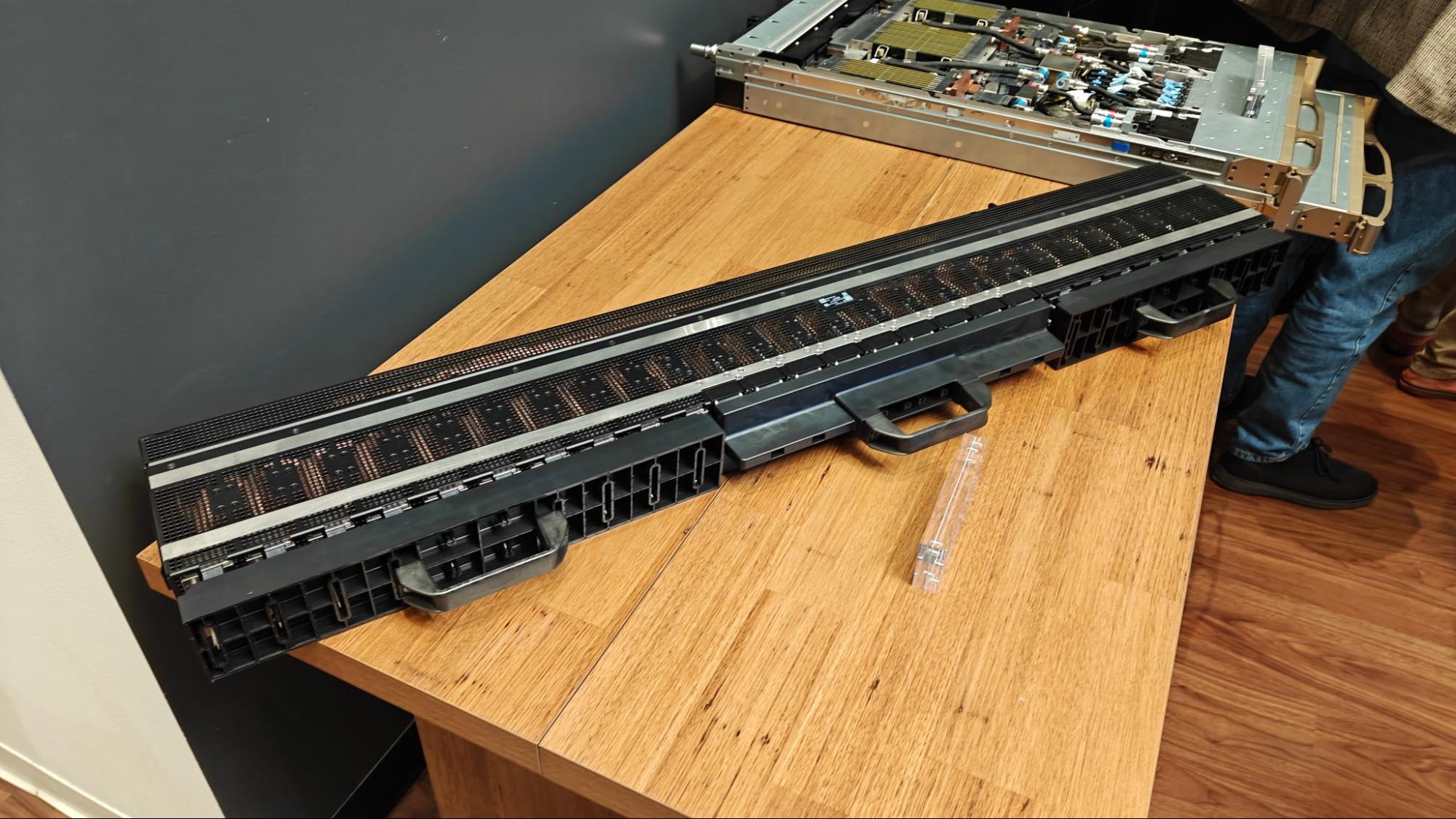
Underpinning scale-up communication is Nvidia’s sixth-generation NVLink, which is deployed as switches in the rack and connected to compute trays using Nvidia’s NVLink spine. You can see the spine on its own in the image above, which features over two miles of thin copper wire to allow every tray in the rack to communicate with each other.
(Image credit: Nvidia)
Localizing storage, networking, security, and telemetry operations is Nvidia’s BlueField-4 DPU. A Vera Rubin NVL72 compute tray includes a single DPU and two ConnectX-9 NICs to maximize CPU/GPU utilization. You can read more about Bluefield 4 in our original coverage from GTC.
Nvidia’s Ian Buck, vice president of hyperscale and high-performance computing and the inventor of CUDA, says the company has “shipped... let's put it in the hundreds of thousands of Grace standalone servers.” In May, Nvidia disclosed that it had shipped over 2.5 million Grace CPUs in total, and the company announced a partnership with Meta to deploy standalone Grace servers in February. Buck’s comments suggest the scale of deployment may be even larger, however, as Nvidia tries to compete in a market dominated by other players.
It’s an interesting comment, though not a surprising one. Nvidia has become the dominating force of Silicon Valley as demand for its GPUs skyrocketed during an unprecedented data center buildout for AI inference. Since peaking earlier this year, however, around $1 trillion in Nvidia’s market cap has been wiped away as investors rally behind CPU makers like Intel. Evolving agentic AI workloads have changed the hardware balance, shifting away from as many as eight GPUs per CPU, toward a one-to-one ratio in some cases.
Nvidia wants to ride that train with its new Vera CPU, which was architected specifically for those types of workloads. Even before the recent rise of agents, however, Nvidia says it has seen demand for its CPUs for data-hungry workloads. “They weren’t running a web server [with Grace]… or they aren’t being used for, what the cloud uses, of cheap, dollar-per-core,” Buck said. “They were being deployed for the backend, data-rich operations, like the data processing.”
Grace represents an on-ramp for Nvidia into data center CPUs. It uses 72 stock Arm Neoverse V2 cores, but it’s differentiated by Nvidia’s Scalable Coherency Fabric (SCF). Vera uses an updated SCF, but it also features Nvidia’s first custom core design, called Olympus. Grace cracked the door, and Vera represents Nvidia's big entrance into the market against AMD and Intel.
Regardless of where Vera ends up in the battle of next-gen data center CPUs — which is heating up now, as AMD is expected to launch its Zen 6 Venice CPUs this week — the design is vastly different from what we’ve seen out of Intel and AMD. Most notably, Vera is monolithic, placing all of its 88 cores on a single piece of silicon. AMD and Intel, years ago at this point, pivoted away from monolithic dies in favor of chiplets, allowing an extremely high density of cores at the cost of latency and coherency issues. Vera is radically different in that regard, not only being built on a single die, but also dedicating significant die space to the fabric.
“One of the reasons we don’t have 128 cores is because we’ve dedicated so much of the die area toward the fabric,” Buck said. “It’s 3.4 TB/s of bandwidth inside of that CPU that is dedicated toward allowing every core to talk to every cache, every memory [controller] at full speed without any collisions.”
For clarification’s sake, Buck is referencing 3.4 TB/s of core-to-core bandwidth in Vera. There’s up to 1.2 TB/s of aggregate memory bandwidth (14 GB/s per core) through the LPDDR5X interface.
But just as chiplet-based designs made trade-offs in per-thread performance, Vera will likely make trade-offs for its unique architecture. The majority of data center workloads are still “legacy” tasks that hyperscalers have built for, and even with seemingly insatiable demand for AI infrastructure, that is unlikely to change for several years.
Buck recognizes this trade-off, asking: “Can Intel and others build rich fabrics? Do they have the IP and the ecosystem to do it and connect it all the way through to LP memory? They need to tell you when they’re going to do it… but that trade-off will come at the cost of the legacy workload.” Earlier this year, at GTC in March, Buck was even more clear. “The world is not going to be served by one SKU of CPU, and that is not our intention,” the executive said in a news conference at the time.
Still, it’s clear Nvidia has ambitions with data center CPUs beyond what headlines are floating around on the New York Stock Exchange. Nvidia says CPUs represent a $200 billion TAM (Total Addressable Market) opportunity for the company, a rather rosy forecast compared to the rest of the industry, which sees a TAM of around $120 billion by 2030 (though recent estimates have climbed as high as $170 billion). And agentic AI is expanding that market, with Morgan Stanley in April estimating that agents could add as much as $60 billion to the data center CPU market.
Vera is in full production alongside Nvidia’s next-gen AI infrastructure, including Rubin GPUs, ConnectX-9 NICs, SpectrumX Ethernet switches, and the various components that go into building a Vera Rubin NVL72 rack. The company says there are around 1.3 million components that go into a rack, and it has a list of over 300 partners globally to build them. As part of our visit to Nvidia HQ last week, we saw a Vera Rubin NVL72 rack in action, running workloads for OpenAI.
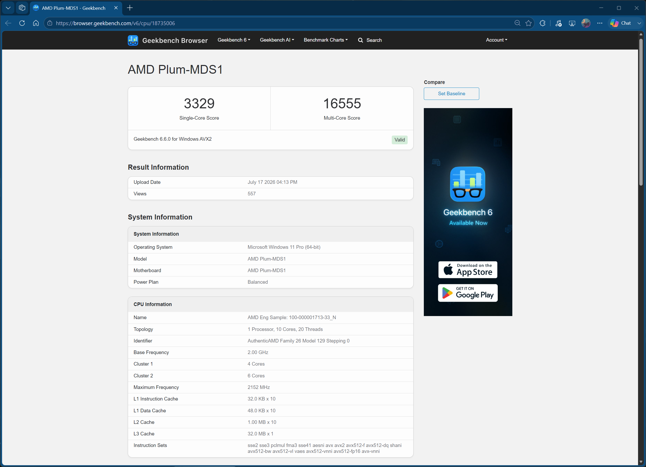
AMD is expected to refresh both its desktop and mobile lineups with Zen 6 next year. Ryzen AI 500 series, codenamed Medusa Point, will be the company's next-gen mobile family and we've already seen a 10-core part leak from it a couple of times. Now, that same SKU is back with another Geekbench listing, this time posting its best results that put it ahead of any mobile chip currently made by Intel or AMD (in one way).
(Image credit: Future)
AMD's upcoming chip ended up scoring 3,329 points in the single-core test and 16,555 points in the multi-core test. The Geekbench page once again shows the platform name as "AMD Plum-MDS1," which we've known to be associated with Medusa Point for a while now. The SKU is listed as "AMD Eng Sample 100-000001713-33_N," which is identical to how we saw in the last leak, basically confirming we're looking at the same chip.
The single-core result is almost 5% higher while the multi-core score is about 9.7% higher compared to the numbers we saw previously. In fact, the single-core result is better than any mobile part on Geekbench apart from the new Snapdragon X2 Elite lineup. Compared to desktop equivalents, it's very close to the 9900X and the 9800X3D — two absolute desktop powerhouses carrying 12 cores and 8 cores, respectively.
SKU
Config
Single-Core Score
Difference
Qualcomm X2 Elite X2E-90-100
Mobile, 18C
3,573
100%
AMD Ryzen 9 9900X
Desktop, 12C
3,333
93%
AMD Ryzen 7 9800X3D
Desktop, 8C
3,333
93%
AMD Ryzen 9 565?
Mobile, 10C
3,329
93%
AMD Ryzen 5 9600X
Desktop, 6C
3,318
93%
Intel Core i9-14900KS
Desktop, 24C
3,226
90%
Intel Core Ultra 9 285K
Desktop, 24C
3,195
89%
AMD Ryzen 9 565? (Previous)
Mobile, 10C
3,174
89%
The multi-core score puts this 10-core SKU right alongside the Ryzen AI Max+ 390, which is just a tier below the top-end AI Max+ 395 from Strix Halo. Since this is a 10-core part, we can infer it's the Ryzen AI 9 565 because the Ryzen AI 9 365 (from Strix Point) and Ryzen AI 9 465 (from Gorgon Point) share the same configs. The Ryzen AI 9 365 has an average score of 12,410, so Medusa Point's offering is 33% faster in this regard.
SKU
Config
Multi-Core Score
Difference
Qualcomm X2 Elite X2E-90-100
Mobile, 18C
18,026
78%
AMD Ryzen 9 9950X3D
Desktop, 16C
22,169
96%
AMD Ryzen 9 9900X
Desktop, 12C
19,696
86%
AMD Ryzen 7 9800X3D
Desktop, 8C
18,317
80%
AMD Ryzen 9 565?
Mobile, 10C
16,555
72%
AMD Ryzen 5 9600X
Desktop, 6C
14,742
64%
Intel Core i9-14900KS
Desktop, 24C
23,008
100%
Intel Core Ultra 9 285K
Desktop, 24C
22,472
98%
AMD Ryzen 9 565? (Previous)
Mobile, 10C
15,092
66%
The Geekbench listing also reports the correct clock speeds this time — 2.0 GHz is still lasted as the base frequency, but the boost frequency is marked at 5.37 GHz, which makes a lot more sense. Moreover, the listing shows 10MB of L2 cache and 32MB of L3 cache while the Ryzen AI 9 465 had a combined cache tally of 34MB.
Overall, this benchmark is an incredibly promising showing for Medusa Point. The Red Team's next-gen mobile lineup seems to benefit heavily from an architectural jump thanks to the Zen 6 silicon. Keep in mind that this is the company's mainstream mobile offering that's supposed to compete with Intel's Panther Lake, while Nova Lake mobile and AMD's own Gator Range (Ryzen 10000) will serve only as high-end CPUs.
The Zilog Z80 has just turned 50 years old. This iconic 8-bit processor first went on sale in July 1976 and stayed in production for 48 years until Zilog, now a Littelfuse subsidiary, stopped accepting orders in June 2024. However, there’s an open-source replacement closer than ever to shipping in the chip’s original 40-pin DIP package thanks to community-funded fabrication.
The original Z80 packed 8,500 transistors on a 4μm process and typically ran at 2.5 MHz, with later CMOS variants reaching 20 MHz. Binary compatibility with the Intel 8080 let it absorb the existing CP/M software base, with an on-die DRAM refresh counter that cut the number of support chips a system needed. Development of working prototypes cost roughly $400,000 against $500,000 in funding from Exxon, per the Computer History Museum.
The chip powered the ZX Spectrum, TRS-80, MSX machines, Nintendo's Game Boy, Sega's Master System, the Pac-Man arcade cabinet, and Texas Instruments' graphing calculators, then shipped in industrial controllers for decades after home computing moved on to more powerful successors. Zilog's end-of-life notice, dated April 15, 2024, told customers its wafer foundry was discontinuing support for the Z84C00 family, and last-time-buy orders closed that June.
However, Renaldas Zioma's FOSS Z80 project, launched shortly after the end-of-life notice, now has working silicon. The first version, fabbed on SkyWater's 130nm node through Tiny Tapeout 7 on a die of just 0.064mm2, has been confirmed as functional via the project’s GitHub repository. A QFN64 version with all 40 pins exposed followed on the Efabless CI2406 shuttle, two further runs then went through IHP's 130nm process, and the current run targets the classic DIP40 form factor using chip-on-board assembly on GlobalFoundries' 180nm GF180MCU node via Wafer.Space. The end goal here is to fab a drop-in replacement for machines like the ZX Spectrum and RC2014 kits.
The design is built around Guy Hutchison's TV80 Verilog core, and the project's Tiny Tapeout page says the 130nm CMOS implementation should support clocks up to 50 MHz, against 4 MHz for the original NMOS part.
Zilog is trimming the Z80's official successor line as well. A product change notification from last October put the eZ80L92, along with several Z8F-series microcontrollers, on end-of-life, citing "little to no demand." Last-time-buy orders closed on January 20 this year, with shipments scheduled through April 20, on non-cancelable, non-returnable terms. The eZ80L92 is the only eZ80 part named in the notice; the pipelined eZ80 architecture, introduced in 2001 and still inside TI's current TI-84 Plus CE calculators, otherwise remains in Zilog's catalog.
Hobbyists keep finding work for the original chip regardless. For example, earlier this year, a developer ran a tiny conversational AI on a Z80 with 64KB of RAM.
AMD launched the Ryzen 7 7700X3D a couple of days ago to universal acclaim, with reviews praising its consistently excellent gaming performance while critiquing the price point. It's officially priced at $329, which is just shy of what the Ryzen 7 7800X3D goes for these days, rendering the newest X3D chip a bit pointless. However, thanks to a new promo code on Newegg, you can purchase it for as low as $279 right now.
Just add the CPU to your cart, and at checkout, the promo code "PKC337" will be automatically applied to give you a $49 discount. That should bring the price down to just $279 before tax. At that price, the Ryzen 7 7700X3D suddenly becomes much more feasible thanks to its improved value proposition. Now, there's at least $120 separating the Ryzen 7 7700X3D from the Ryzen 7 7800X3D, freeing up money you can put toward other upgrades.
For context, both chips are essentially the same; you can look at the Ryzen 7 7700X3D as the binned-down version of the Ryzen 7 7800X3D silicon that couldn't be used for the more expensive SKU. Both are 8-core, 16-thread parts with 104MB of combined cache and 120W TDPs. The Ryzen 7 7700X3D can boost up to 4.5 GHz, while the Ryzen 7 7800X3D has a 5 GHz boost clock. That's enough to just barely edge the Ryzen 7 7700X3D in gaming performance.
On the other hand, if you're looking for an all-rounder that also excels in professional workloads, then Intel's latest Arrow Lake refresh chips are better. Both the Core Ultra 5 250K Plus and the Core Ultra 7 270K Plus are faster at productivity tasks than the Red Team's offerings in the same class. But now that there's a clear price distinction among them, the Ryzen 7 7700X3D makes sense if you're just gaming.
The Ryzen 7 7700X3D is also a Newegg exclusive in North American markets till Q4 2026 so it makes sense that the retailer can discount it this quickly. The Ryzen 7 7800X3D is also on sale, but it has not received any promo codes on the site as of now. So, if you're looking to finally jump on the X3D train and on the AM5 socket, but don't want to spend over $300, this is your chance to grab the Ryzen 77700X3D for as low as $279.
Thanks to the ongoing component crisis caused by the AI boom, it's a particularly difficult time to build a gaming PC. Despite ample supply, most parts are overpriced, forcing consumers to resort to patience or finding deals. We've done the latter and found an enticing AM4 bundle on Newegg consisting of a Ryzen 7 5800X3D, 16GB of DDR4 RAM, and a feature-rich B550 motherboard — all for just $529.99 right now. You'll be saving over $100 in this combo compared to buying these items separately.
The star of the show is the Ryzen 7 5800X3D, the CPU that kickstarted AMD's gaming dominance, as it was the first X3D chip the company ever made. Newegg is bundling the 10th Anniversary Edition here with a Carbide Ice Pad that you can use in place of thermal paste. The specs remain unchanged; it's an 8-core processor with 16 threads that can boost up to 4.5 GHz. It has a total cache of 100MB, 64MB of which is the extra L3 cache stacked atop the CCD, and a 105W TDP.
Then there's the motherboard, which is an Asus TUF Gaming B550-Plus Wi-Fi II. As the name suggests, it's a full-sized (ATX) AM4 motherboard using the B550 chipset. It features a robust 8+2 phase VRM for power delivery. There are four DDR4 RAM slots onboard, along with two M.2 slots, including one PCIe 4.0-capable. The board has Wi-Fi 6, 2.5 Gbps Ethernet, USB 3.2 Type-A and Type-C, and more in terms of connectivity. You also get 2x ARGB headers.
The fastest DDR4 CPU on the market that can still hold its ground against DDR5 options, paired with enough RAM and a solid motherboard to get your gaming journey started.View Deal
Finally, we have the RAM, which is by far the hardest component to source for a reasonable price these days. Thankfully, you're getting a solid kit from TeamGroup here: T-Force Delta RGB 16GB (8x2) DDR4-3200 running at CL16. This combination strikes a great balance for AM4, and since X3D chips rely more on their extra 3D V-Cache, even slightly slower RAM doesn't lose performance. Not to mention, this kit has some nice-looking RGB, too.
Newegg is bunding all of these parts together for just $529.99, but they'll cost you a lot more separately. We put the CPU, RAM, and motherboard on PCPartPicker and got a total of $629 before tax, which means you're saving about $100 by choosing this bundle. And it's not like these are bargain-bin components either, you're getting basically the best that DDR4 and AM4 have to offer, but without breaking the bank.
Intel was expected to unveil its next-generation desktop processors later this year. The upcoming Nova Lake lineup has been making the rounds online, and a new report from VideoCardz suggests that Intel could introduce it under the Core Ultra Series 400 branding. For context, the current Arrow Lake and Arrow Lake Refresh desktop CPUs follow the Core Ultra Series 200 naming scheme, while Intel's latest Panther Lake mobile processors carry the Core Ultra Series 300 branding.
The report also claims to reveal the review embargo windows and launch timeline for several Nova Lake models. According to the report, Intel will initially introduce a 28-core DS package, which is expected to launch between January and March 2027. The new DS suffix is said to be an internal package designation for processors featuring dual-compute tiles. This will reportedly be followed by 28-core K-series (unlocked) models between March and April 2027, while 16-core and 8-core variants are expected to arrive between late March and May 2027. The flagship 52-core DS model is reportedly scheduled for a much later launch, potentially between late May and September 2027.
Rumored Nova Lake launch timeline
Processor
P-cores
E-cores
LPE-cores
Expected launch
52-core DS
16
32
4
Late May to September 2027
28-core DS
8
16
4
January to March 2027
28-core K-series
8
16
4
March to April 2027
16-core
4
8
4
Late March to May 2027
8-core
4
4
0
Late March to May 2027
While Intel is yet to officially confirm a launch date for Nova Lake, various leaks have suggested that the lineup could be one of the company's biggest generational leaps in recent years. The flagship desktop SKU, featuring a 52-core configuration, is expected to combine 16 Coyote Cove Performance (P) cores, 32 Arctic Wolf Efficiency (E) cores, and four Low Power Efficiency (LPE) cores. This would be a notable jump over the current Core Ultra 9 285K, which features a total of 24-cores. The introduction of Coyote Cove and Arctic Wolf also points to an entirely new CPU architecture, replacing the Lion Cove and Skymont cores found in Arrow Lake.
Nova Lake is also rumored to bring new platform upgrades including support for DDR5-8000 memory, up to 24 PCIe 5.0 lanes for expansion, Thunderbolt 5, and Intel's next-generation Xe3 Celestial integrated graphics. The processors are also expected to feature an upgraded NPU5 for AI workloads along with a 150W Processor Base Power (PBP) and 253W Maximum Turbo Power (MTP) on the flagship model, despite the substantial increase in core count. Earlier reports have also indicated that Nova Lake will transition to a new LGA1954 socket, meaning users will likely need a new motherboard to upgrade from the existing Arrow Lake platform.
Last month, at Computex 2026, AMD unveiled the Ryzen 7 7700X3D — its brand-new 3D V-Cache chip meant to slot in between the 7600X3D and the 7800X3D. As such, it comes in at a suggested retail price of $329 and, surprisingly, is available exclusively at Newegg in North American markets. It's a capable CPU in a vacuum, almost matching the 7800X3D in gaming while being more efficient in some titles, but it still doesn't provide the best value overall given the existence of the 7600X3D.
The 7700X3D and 7800X3D chips share pretty much identical specs. Both are 8-core, 16-thread CPUs based on the Zen 4 architecture, carrying a combined 104MB of cache. They have the same 120W TDP as well, with a 162W max power limit. The difference lies in the clocks, where the 7800X3D can boost up to 5 GHz; the new 7700X3D is limited to just 4.5 GHz.
When it comes to performance, at 1080p, the 7700X3D is actually the third fastest chip we've ever tested, right behind the 7800X3D and the 9800X3D. The stepped-down 7600X3D is very close to the 7700X3D as well, despite being almost $100 cheaper — this is the 7700X3D's biggest downfall: it's only 2% faster than the much cheaper 7600X3D. In our efficiency geomean, the 7700X3D posted the best FPS per watt results we've ever seen, just edging out the aforementioned 7600X3D.
Productivity is where the 7700X3D takes a hit, as it ranks toward the bottom of our charts when it comes to professional workloads. Intel takes the lead in this department, but it doesn't really matter since no one is buying an X3D chip outside of gaming priorities. If you're looking for an all-rounder, we suggest taking a look at the Core Ultra 250K Plus for around $200 or the Core Ultra 270K Plus for over $300.
The Ryzen 7 7700X3D is available across the world, but we can confirm that Newegg is the only place you can buy it if you're in Canada or the United States. This exclusivity runs through till Q3 2026, so the CPU isn't available even on Amazon or Micro Center — the latter of which has exclusivity for the Ryzen 5 7600X3D, Ryzen 5 7500X3D and the older Ryzen 5 5600X3D in America.
As per our review, the 7700X3D comes within 5% of the 7800X3D's gaming performance, but is only 2% faster than the 7600X3D, which you can buy on Amazon for $239. This makes it a tough sell, but if you're set on grabbing one, Newegg is the place to be.
 登录
登录