Limits on the amount of VRAM on Nvidia's consumer GPUs have forced the modding community to take matters into their own hands. Time and again we've seen various DIY memory upgrades being performed, and it's even offered as a proper repair service in underground markets, but rarely is it done openly. As such, we've just spotted a vendor that will upgrade the 11GB of VRAM on an RTX 2080 Ti to 22GB and provide the BIOS for it upfront — no shady back-alley deals required.
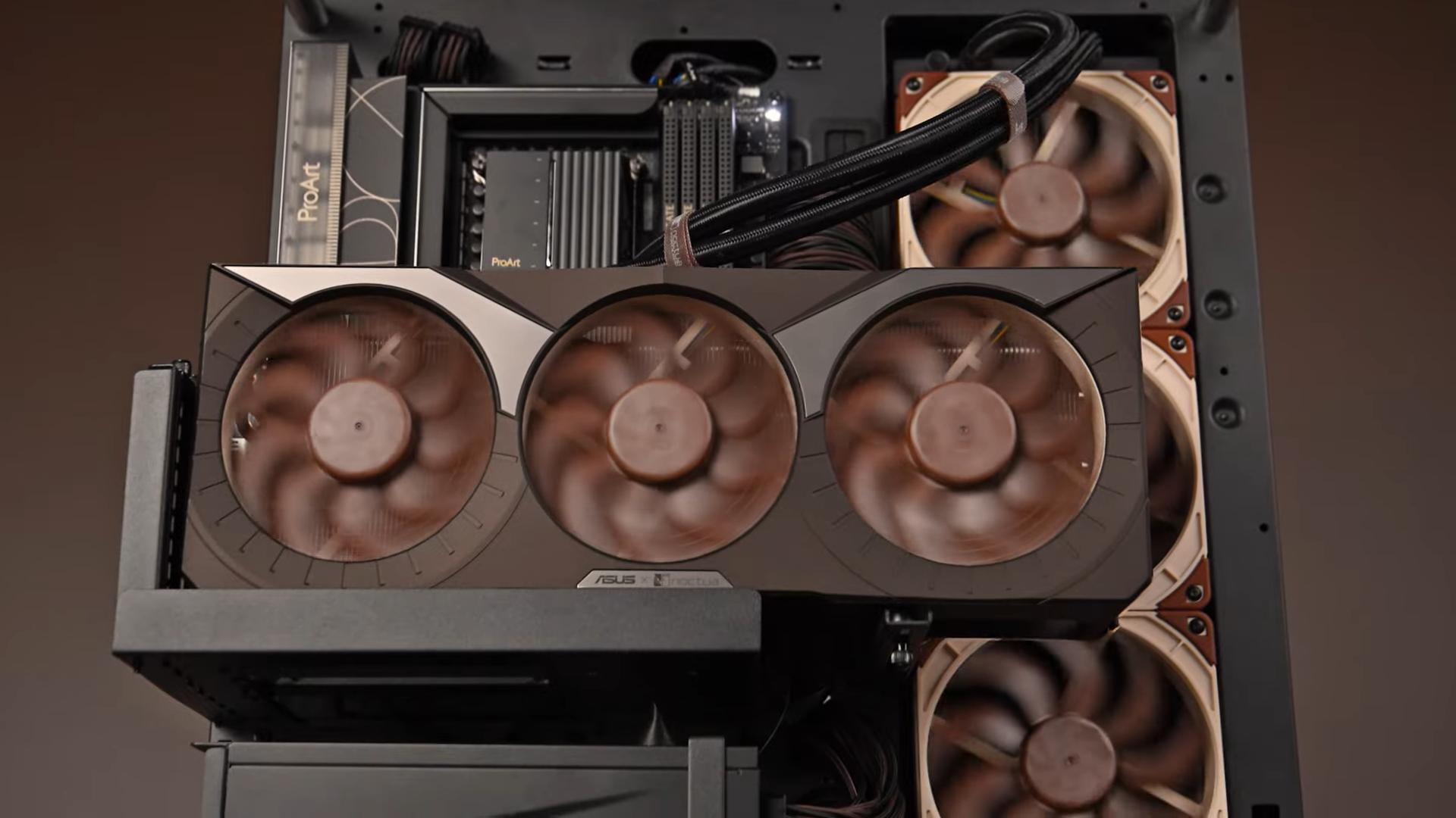
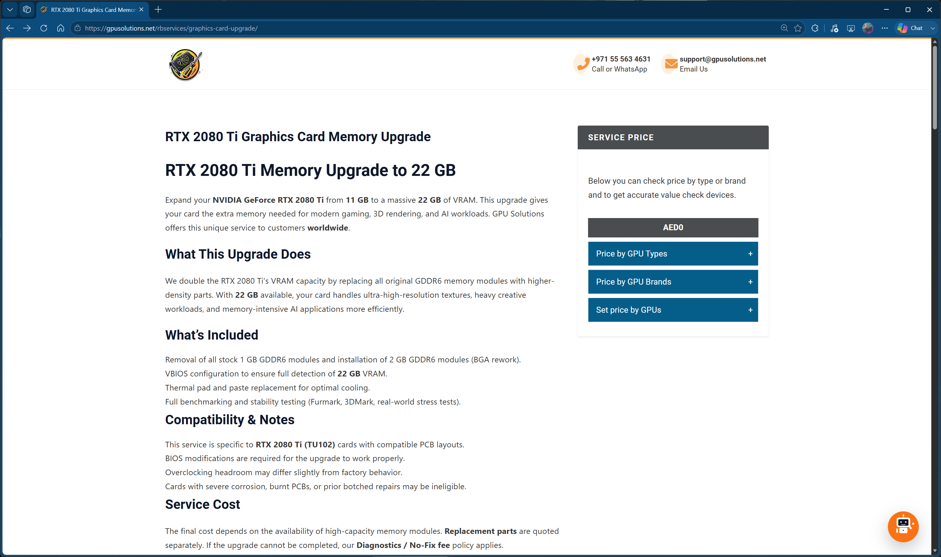
The name of the shop is GPU Solutions (very creative, we know), and it's based in the UAE, though they say they serve customers around the world. On their website, you can select the "Graphics Card Memory Upgrade" service for both the RTX 2080 Ti and the RTX 3070, though the former has more details. These guys also have a YouTube channel where they've already performed the upgrade on an Asus Strix variant before.
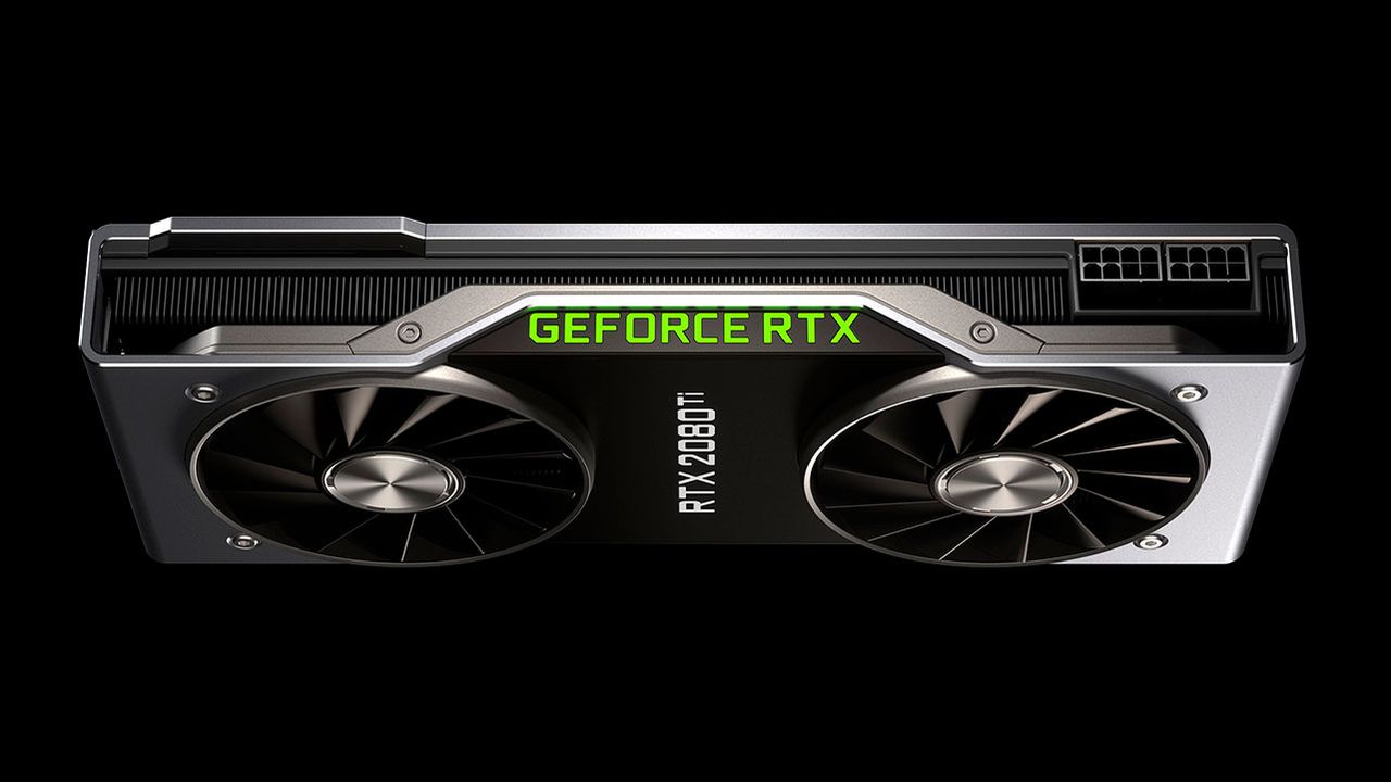
The upgrade works just like any other you might've already seen. The card is disassembled to reach the PCB and remove the preexisting VRAM modules. The RTX 2080 Ti uses 11x 1GB GDDR6 chips, so replacing them with the same amount of 2GB GDDR6 doubles the memory capacity instantly. This is a rather straightforward way of going about a VRAM upgrade, because oftentimes it actually requires a custom PCB.
Once the hardware part of the job is done, the VBIOS is then manually edited to support the new memory pool. This can either be an easy tweak or a lot of work just to get the BIOS to recognize the card, depending on how that specific GPU was built by the manufacturer. For instance, Nvidia was once said to include 16GB of memory with the RTX 3070, but it ended up shipping with 8GB instead, so customizing the BIOS is as simple as unlocking its full potential.
In this case, there wasn't any software tweaking; the core supports multiple memory configs, so the repairperson physically modified the memory strap resistors on the PCB. The original config for the 11GB modules was set to low, low, low. They desoldered and moved the resistors to a new configuration: high, high, and low, which made the GPU recognize and report 22GB of VRAM inside GPU-Z.
(Image credit: Future)
The fact that you get not only double the VRAM on your RTX 2080 Ti but a working, stable BIOS out of the box adds to the overall package significantly. These kinds of mods are usually very hands-on, which means limited to just enthusiasts and tinkerers, but the factory-like service GPU Solution is providing means pretty much anyone can get it done without a hassle.
Their website doesn't mention the charges for an upgrade like this, but considering the ongoing component crisis, the memory modules won't be cheap. They also clarify that the upgrade can only be performed on a card with "compatible PCB layouts." If yours qualifies, they'll also replace the thermal pads and thermal paste accordingly, plus provide substantial benchmarking data to prove the modded card is stable.
Doubling the VRAM should allow you to squeeze a lot more performance out of your 2080 Ti in AI workloads and creative applications such as video editing. It's also helpful in gaming but not to a significant degree since the GPU itself isn't as powerful as modern offerings that are otherwise bottlenecked by memory capacity. Ultimately, this remains a pretty reasonable upgrade because the true, full potential of this GPU was achieved three years ago when someone modded it with an insane 44GB of VRAM.
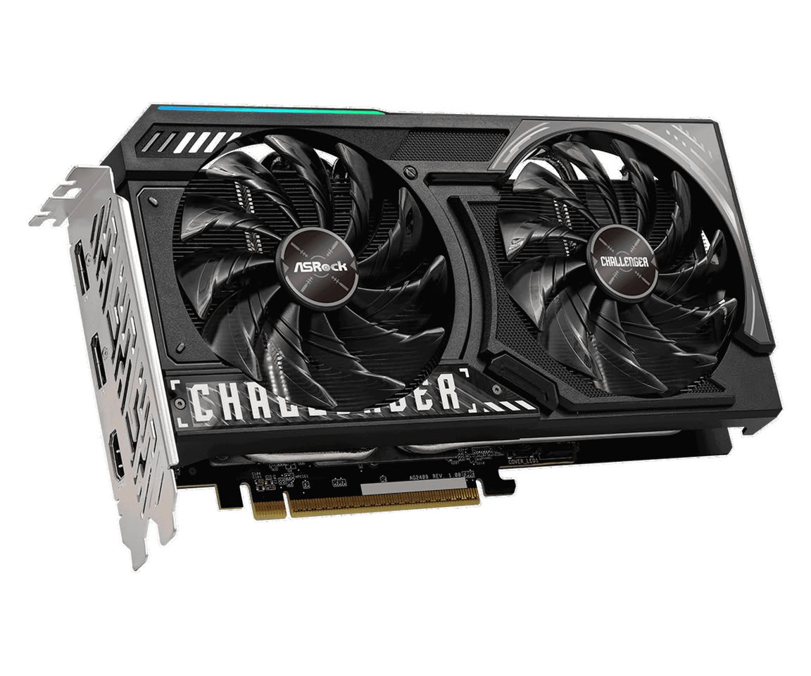
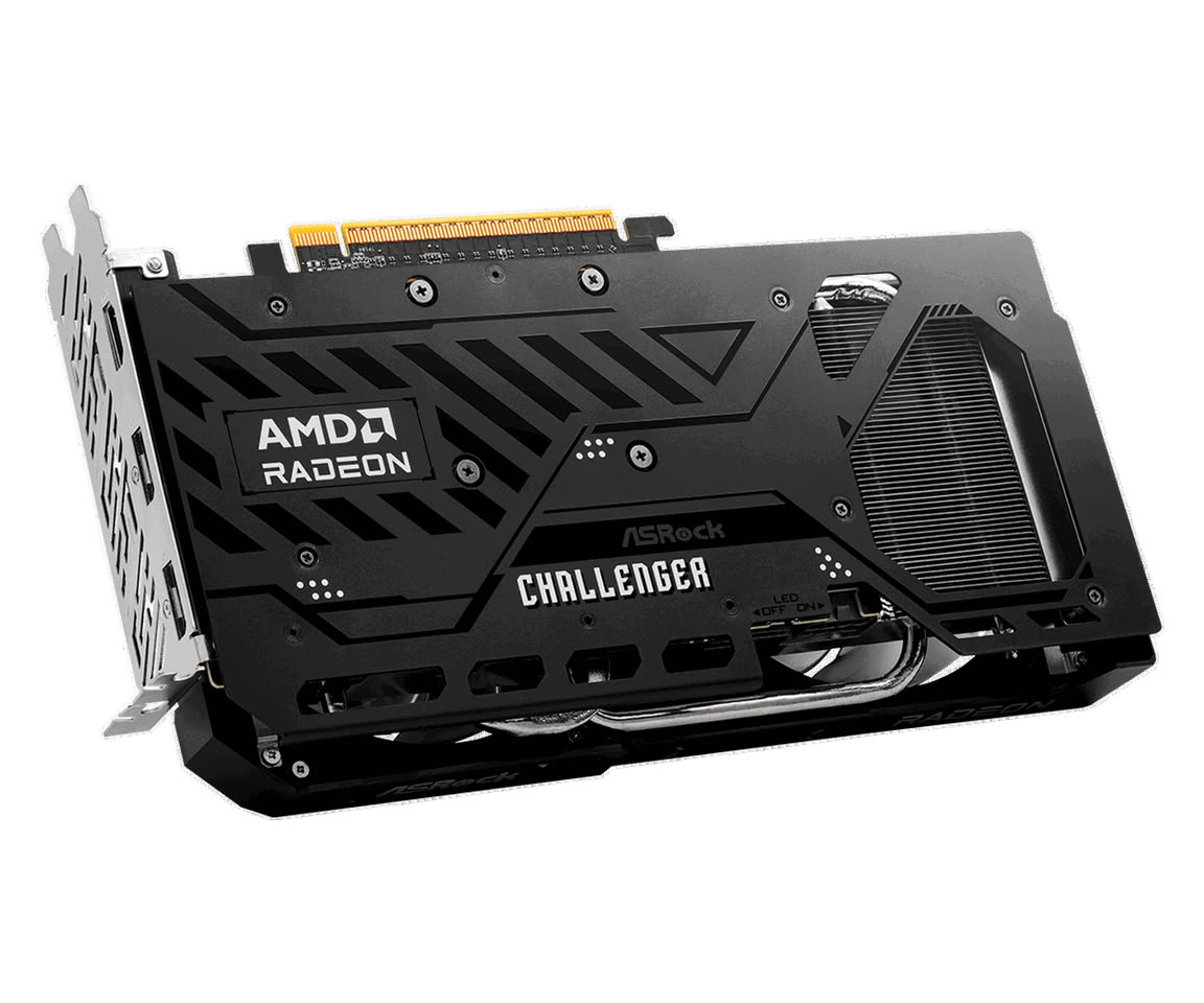
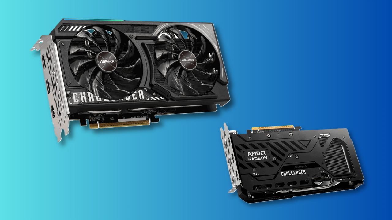
A few months ago, reports of AMD working on a new entry-level GPU began making the rounds, and today we've just got our clearest look yet at the rumored cards.ASRock has just listed the rumored Radeon RX 9050 on its website in two different configurations, 4GB and 8GB, but we have no word on pricing or availability. AMD hasn't made any official announcements yet, so we only have a limited amount of info to dissect, and it should naturally be taken with a grain of salt. However, the leaked specs from an official vendor, which have since been taken down, would herald the return of 4GB VRAM GPUs in 2026, not seen since 2022.
amd hasnt updated the radeon 9000 series family listed on the wesite.asrock rx 9050 4g & rx 9050 8g64bit vs 128biti guess the 8gb card has four 2g chips to reach the full 128bit, while the 4gb card has only two 2g chips, so its only 64bit. would it be better if the 4gb card… https://t.co/yYATuPnioT pic.twitter.com/jX0geYO6uMJuly 28, 2026
The RX 9050 seems to be using a cut-down Navi 44 GPU from the RX 9060 series, with 1,024 cores spread across 16 Compute Units. The leak from May claimed it had 32 CUs instead. ASRock's Challenger variant lists a 1,920 MHz base clock and a 2,600 MHz boost clock. The listing also recommends a 450W power supply, which is 50W less than the RX 9060's 500W recommendation, though we don't know the board power for the RX 9050 yet.
Leaked RX 9050 specs*
SKU
GPU
Cores
Memory (GDDR6)
Memory Bus
Bandwidth
Board Power
AMD Radeon RX 9060 XT 8GB
Navi 44
2,048
8 GB
128-bit
320 GB/s
150W
Intel Arc B580
BMG-G21
2,560
12 GB
192-bit
456 GB/s
190W
NVIDIA GeForce RTX 5060
GB206
3,840
8 GB (GDDR7)
128-bit
448 GB/s
145W
AMD Radeon RX 9060
Navi 44
1,792
8 GB
128-bit
288 GB/s
132W
NVIDIA GeForce RTX 5050
GB207
2,560
8 GB
128-bit
320 GB/s
130W
AMD Radeon RX 9050 8GB
Navi 44
1,024
8 GB
128-bit
288 GB/s
?
AMD Radeon RX 9050 4GB
Navi 44
1,024
4 GB
64-bit
144 GB/s
?
Intel Arc A310
ACM-G11
768
4 GB
64-bit
124 GB/s
30W
NVIDIA GeForce GTX 1630
TU117
512
4 GB
64-bit
96 GB/s
75W
Those were the mutual specs between both variants — the only difference lies in the memory config. The 4GB variant listing notes 4GB of GDDR6 VRAM operating over a 64-bit bus, giving us a bandwidth of 144 GB/s. We haven't seen a 4GB memory pool in GPUs since 2022, when Intel's Arc A310 and Nvidia's GTX 1630 came out. All current-gen cards have adopted 8GB as a baseline, which already gets criticized for not being future-proof.
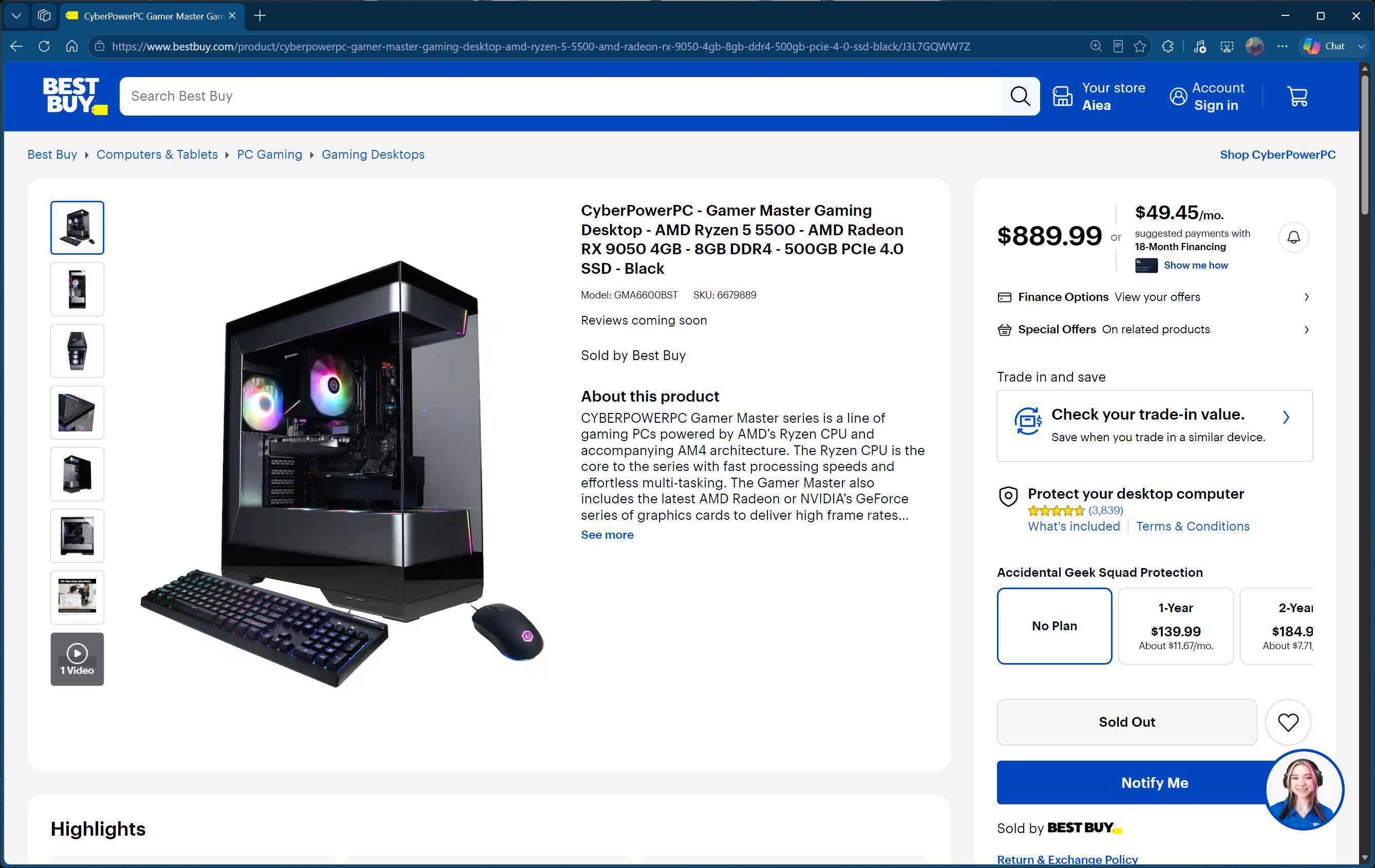
The 8GB variant specs listed would double the bandwidth to 288 GB/s thanks to its 128-bit-wide bus. There's a chance AMD is planning to sell the 8GB to consumers directly while keeping the 4GB variant limited to OEMs. We can't say for sure since ASRock is listing it as a Challenger card on its website, but things could always change. We did find the 4GB RX 9050 already included in a CyberPower prebuilt on Best Buy, though, currently listed for $900.
(Image credit: Future)
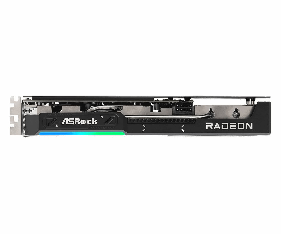
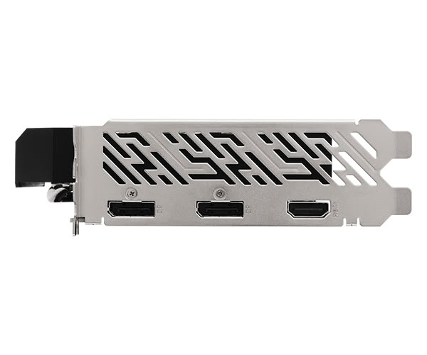
The design in the leaked images appears rather generic: a black shroud with silver accents and some RGB lighting. They show two DisplayPort 2.1a and one HDMI 2.1b ports, and the card is powered via a single 8-pin PCIe connector. In terms of performance, the 8GB model should cruise through 1080p gaming, especially with the help of FSR 4. Since this is an RDNA 4 GPU, you get the full benefits of the architecture, including better ray tracing and upscaling tech.
As mentioned earlier, the last GPUs to ship with 4GB of VRAM were released four years ago. The industry is going through a turbulent period given the ongoing component crisis and memory shortage, but this would be another level of desperation.
The ongoing component crisis has forced manufacturers to raise product prices around the world, which includes the best GPUs. MSI and PNY have just announced new prices for all RTX 50-series graphics cards for China, representing up to a 59% hike compared to MSRP. While Nvidia GPUs have been the most affected, offerings from Intel and AMD are also experiencing a similar predicament, according to Wccftech.
MSI's price list actually shows the old prices (from a week ago) as well as the new ones, giving us an official percentage difference of 10-20%. Keep in mind the old prices still weren't at MSRP. The RTX 5080 Shadow 3X OC/Ventus sees the biggest change, going from 10,000 Yuan ($1,477) to 12,000 Yuan ($1,773), constituting a 20% hike. Other RTX 5080 variants received a pretty similar 18% hike, while the RTX 5070 Ti Shadow 3X OC now costs 19.5% more.
Product Name
Original Price
Updated Price
Official MSRP
vs. Original
vs. Base MSRP
GeForce RTX 5090 D v2 24G VENTUS 3X OC
¥22,999
¥25,999
¥16,499
+13.04%
+57.58%
GeForce RTX 5080 16G GAMING TRIO OC WHITE
¥10,999
¥12,999
¥8,299
+18.18%
+56.63%
GeForce RTX 5080 16G GAMING TRIO OC
¥10,999
¥12,999
¥8,299
+18.18%
+56.63%
GeForce RTX 5080 16G SHADOW 3X OC/VENTUS
¥9,999
¥11,999
¥8,299
+20.00%
+44.58%
GeForce RTX 5070 Ti 16G GAMING TRIO OC
¥8,199
¥9,699
¥5,499
+18.29%
+76.38%
GeForce RTX 5070 Ti 16G SHADOW 3X OC
¥7,699
¥9,199
¥5,499
+19.48%
+67.28%
GeForce RTX 5070 12G GAMING TRIO OC
¥5,899
¥6,399
¥4,499
+8.48%
+42.23%
GeForce RTX 5070 12G VENTUS 3X OC
¥5,499
¥5,999
¥4,499
+9.09%
+33.34%
GeForce RTX 5070 12G SHADOW 3X OC
¥5,499
¥5,999
¥4,499
+9.09%
+33.34%
GeForce RTX 5070 12G SHADOW 2X OC
¥5,299
¥5,799
¥4,499
+9.44%
+28.90%
GeForce RTX 5060 Ti 16G GAMING TRIO OC
¥4,599
¥4,999
¥3,199
+8.70%
+56.27%
GeForce RTX 5060 Ti 16G SHADOW 2X OC PLUS
¥4,299
¥4,699
¥3,199
+9.30%
+46.89%
GeForce RTX 5060 Ti 8G SHADOW 2X OC PLUS
¥3,099
¥3,399
¥2,799
+9.68%
+21.44%
GeForce RTX 5060 Ti 8G GAMING TRIO OC WHITE
¥3,399
¥3,699
¥2,799
+8.83%
+32.15%
GeForce RTX 5060 Ti 8G GAMING TRIO OC
¥3,399
¥3,699
¥2,799
+8.83%
+32.15%
GeForce RTX 5060 Ti 8G INSPIRE 2X OC
¥3,199
¥3,499
¥2,799
+9.38%
+25.01%
GeForce RTX 5060 Ti 8G VENTUS 3X OC
¥3,299
¥3,599
¥2,799
+9.09%
+28.58%
GeForce RTX 5060 8G GAMING TRIO OC WHITE
¥2,799
¥3,199
¥2,199
+14.29%
+45.48%
GeForce RTX 5060 8G GAMING TRIO OC
¥2,799
¥3,199
¥2,199
+14.29%
+45.48%
GeForce RTX 5060 8G GAMING OC V1
¥2,699
¥3,099
¥2,199
+14.82%
+40.93%
GeForce RTX 5060 8G SHADOW 2X OC
¥2,599
¥2,999
¥2,199
+15.39%
+36.38%
GeForce RTX 5050 8G GAMING OC
¥2,599
¥2,999
¥1,899
+15.39%
+57.93%
GeForce RTX 3050 VENTUS 2X E 6G OC
¥1,649
¥1,899
¥1,399
+15.16%
+35.74%
The highest-end Blackwell GPU available in China, the RTX 5090 D V2 is a cut-down version of the RTX 5090, featuring 24GB of VRAM instead of 32GB. MSI raised its price by 13%, which is less than every RTX 5060 and RTX 5050 variant — those were around 14-15%. The RTX 5060 Ti (8GB and 16GB) and RTX 5070 both received price hikes under 10% compared to their old prices.
If you put these numbers up against these GPUs' MSRPs then the picture becomes a lot grimmer. The RTX 5070 Ti Gaming Trio OC is now priced 76% above MSRP, while its cheaper Shadow 3X OC variant is still 67% more expensive than the suggested retail price. The prices for the RTX 5090 D V2 are 57.5% higher, the RTX 5080 and 5060 Ti up to 56% higher, the RTX 5060 up to 45% higher, and the RTX 5070 up to 42% higher.
Moving onto Colorful's list, the company doesn't provide old prices to compare against, so we can only reference them against the MSRPs. The top-end offering, the RTX 5080 Vulcan W OC is now priced 59% above MSRP, while the 5070 Ti Vulcan W OC is 58.5% higher. The RTX 5070 and 5060 Ti 16GB models were largely under the 50% threshold, while price hikes for the RTX 5060 Ti 8GB and RTX 5060 variants were under 30% compared to MSRP.
GPU Model
New Price
Original Price
Difference
% vs MSRP
RTX 5080 Vulcan W OC 16G
¥13,199
¥8,299
+¥4,900
+59.0%
RTX 5080 Vulcan OC 16GB
¥12,299
¥8,299
+¥4,000
+48.2%
RTX 5080 Advanced OC 16G
¥11,799
¥8,299
+¥3,500
+42.2%
RTX 5080 Ultra W OC 16G
¥10,499
¥8,299
+¥2,200
+26.5%
RTX 5070 Ti Vulcan W OC 16G
¥9,999
¥6,299
+¥3,700
+58.7%
RTX 5070 Ti Advanced OC 16G
¥9,299
¥6,299
+¥3,000
+47.6%
RTX 5070 Ti Ultra W OC SFF 16G
¥8,899
¥6,299
+¥2,600
+41.3%
RTX 5070 Ti Ultra OC SFF 16G
¥8,799
¥6,299
+¥2,500
+39.7%
RTX 5070 Ti Deluxe SFF 16G
¥8,699
¥6,299
+¥2,400
+38.1%
RTX 5070 Vulcan X OC 12G
¥7,199
¥4,599
+¥2,600
+56.6%
RTX 5070 Ultra OC 12G
¥6,799
¥4,599
+¥2,200
+47.9%
RTX 5070 Deluxe 12G
¥6,399
¥4,599
+¥1,800
+39.2%
RTX 5060 Ti Ultra W OC 16G
¥5,299
¥3,599
+¥1,700
+47.3%
RTX 5060 Ti Ultra Z OC 16G
¥5,249
¥3,599
+¥1,650
+46.0%
RTX 5060 Ti Ultra OC 16G
¥5,249
¥3,599
+¥1,650
+46.0%
RTX 5060 Ti Deluxe 16G
¥5,199
¥3,599
+¥1,600
+44.6%
RTX 5060 Ti Ultra W DUO OC 16G
¥5,099
¥3,599
+¥1,500
+41.8%
RTX 5060 Ti Ultra DUO OC 16G
¥5,099
¥3,599
+¥1,500
+41.8%
RTX 5060 Ti Advanced OC 8G
¥3,949
¥3,199
+¥750
+23.5%
RTX 5060 Ti Ultra W OC 8G
¥3,949
¥3,199
+¥750
+23.5%
RTX 5060 Ti Ultra OC 8G
¥3,849
¥3,199
+¥650
+20.3%
RTX 5060 Ti Deluxe 8G
¥3,699
¥3,199
+¥500
+15.7%
RTX 5060 Ti DUO 8G
¥3,549
¥3,199
+¥350
+11.0%
RTX 5060 Advanced OC 8G
¥3,199
¥2,499
+¥700
+27.9%
RTX 5060 Ultra W OC 8G
¥3,149
¥2,499
+¥650
+26.0%
RTX 5060 Ultra DUO OC 8G
¥3,049
¥2,499
+¥550
+22.0%
RTX 5060 Deluxe 8G
¥3,049
¥2,499
+¥550
+22.0%
RTX 5060 DUO 8G
¥2,949
¥2,499
+¥450
+17.9%
RTX 5050 DUO 8G
¥2,449
¥2,099
+¥350
+16.8%
Both of these lists came directly from the distributors but marketplaces online show that AMD and Intel GPUs are also more expensive now, as well. AMD's cards are selling for 14% to 29% higher prices, and Blue Team's cards are seeing $200 to almost $300 bumps, according to Wccftech. The RX 9060 XT 16GB is the worst offender among the two lineups, being hiked up by 28.8% compared to its MSRP.
All of this is happening because VRAM prices have skyrocketed over the past year, with reports highlighting a $20 price increase per module. That means an 8GB card, with taxes included, should cost almost $100 more now, a 12GB card about $130 more, and a 16GB card roughly $180 more, and that's just accounting for VRAM price changes. With prices going up, there's an additional element of supply and demand that is pushing prices higher.
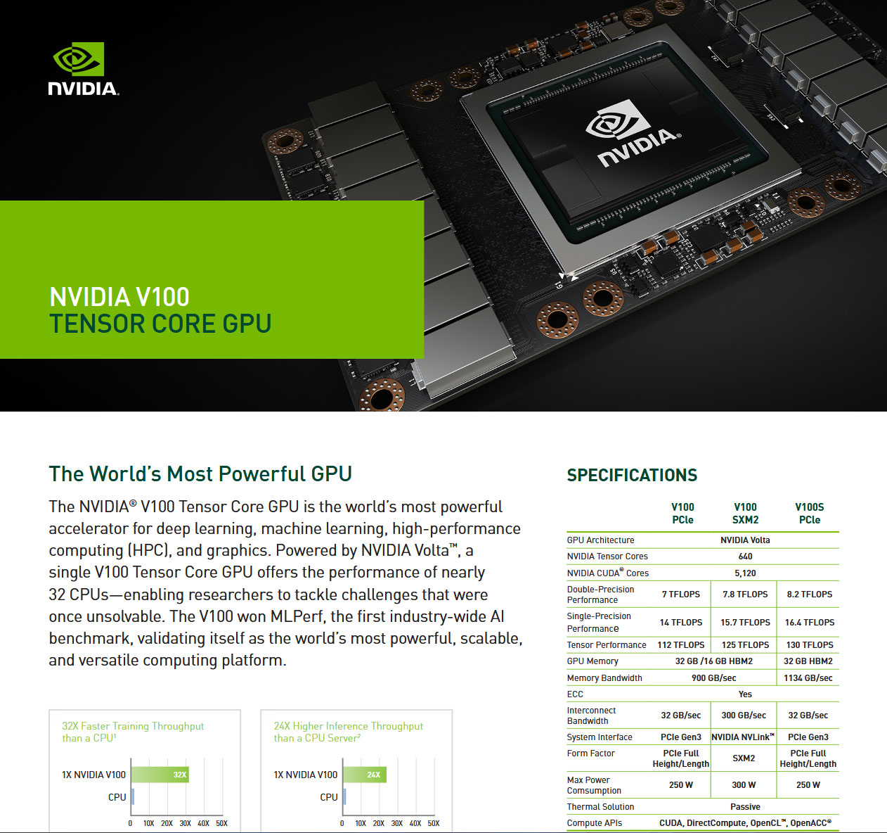
A computing enthusiast has repurposed a very noisy and largely obsolete enterprise GPU (with lots of VRAM) for local LLM inference purposes. They are now enjoying a system that has doubled its total VRAM quota to 32GB for just a $266 (£200) outlay. That’s a good result, especially in the midst of a RAMpocalypse.
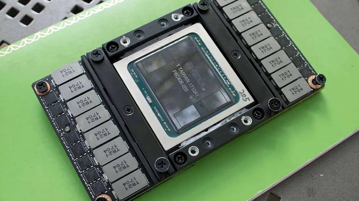
Oscar Molnar explains that a cheap Tesla V100 SXM2 with 16GB HBM2 was sourced, as was an SXM2-to-PCIe adapter, and a PWM mod for the loud-as-a-lawnmower cooler, to complete this VRAM expansion for the hefty local LLMs project. Indeed, these GPUs do look cheap right now, as I can see them listed on eBay US for under $140 each, if you don’t mind buying from China.
As mentioned above, you can’t just get one of these Tesla V100 SXM2 cards with abundant VRAM and plug it into your PC. Molnar says they spent about $66 on an SXM2-to-PCIe adapter, also on eBay.
You might think that was enough. However, the PC and local LLMs enthusiast baulked at the noise of “the fan from hell,” which came as standard with the Tesla V100 SXM2. That shrieking cooler was measured outputting 82dB of noise. Molnar described it as “somewhere between a garbage disposal and a lawnmower.” This may be the most complicated tweak yet, but basically the existing fan wires just needed rerouting and plugging into the motherboard PWM fan header. You could also simply purchase a “2.54mm male to PH2.0 female jumper cable” for the task. Apparently, the fan only needs to run at 10% to keep the Tesla V100 under 50C at full load.
(Image credit: Nvidia)
27 billion parameter LLM runs at 32 tokens per second
With the hardware all now fitted and finessed, Molnar had a 32GB VRAM system at their disposal – that’s a PC with RTX 4080: 16GB VRAM, Ada architecture and Tesla V100: 16GB VRAM, Volta architecture. They note you can get Tesla V100s with 32GB of VRAM, but they are double the price.
Getting the system to make use of this 32GB of total VRAM for LLMs wasn’t tricky, says the DIYer. They used NixOS with a legacy Nvidia driver that overlapped support for both Volta and Ada architectures. Testing a local LLM, they got a 27 billion parameter model running at 32 tokens per second, which they say is “fast enough for interactive use” and faster than most cloud API alternatives.
On this day in 2006, AMD confirmed its acquisition of graphics chip firm ATI. AMD stumped up a cash and stock deal worth a total of $5.4B for the Canadian PC graphics innovators. With 20/20 vision now 20 years on, we can see the deal helped AMD prosper on three fronts: continuation and innovation of Radeon GPUs, the rise of the APU, and AMD’s dominance in the console business. That’s not all, of course, and it is also interesting to recall that AMD approached Nvidia before it bought ATI.
AMD CEO Hector Ruiz and ATI CEO Dave Orton appeared together in New York on the morning of July 24, 2006, to publicly announce the deal. Ruiz told the press that the deal, unanimously approved by the directors of both companies, would "reinvent our industry." The AMD CEO went on, “We believe AMD and ATI will drive growth and innovation for the entire industry, enabling our partners to create differentiated solutions and empowering our customers to choose what is best for them.” Orton added that “Joining with AMD will enable us to innovate aggressively on the PC platform.”
In the next couple of years, the ATI graphics brand slowly melted away. For example, the ATI R600 (Terascale 1, unified shader architecture) GPU, which was in development at the time of the acquisition, would become the Radeon HD 2900 series under AMD branding. As a transition product, some HD 2900 XT boxes would still carry ATI packaging and branding. Taking the cooling solution off an AMD graphics card, you might still see an ATI GPU under the thermal paste, all the way up to around 2010. In 2011, Tom’s Hardware published its 25 Years Of Graphics History: A Farewell To ATI, In Pictures, which is a must-read for fans of the era.
Fully AMD branded (Image credit: Tom's Hardware)
While graphics card development rolled on in a tit-for-tat battle with Nvidia, AMD’s next fortuitous chunk of synergy came from integrating its Radeon IP alongside its CPU cores to create APUs. It started this journey with the AMD Fusion line in 2011. Nowadays we have APUs that have taken this vision far further, with the Ryzen AI Max / Max+ (Strix Halo and Gorgon Halo) series. The integrated graphics on these processors pack up to 40 RDNA 3.5 Compute Units and can go toe-to-toe with desktop graphics like the RTX 4060/4070, depending on workload. They also benefit from unified memory, allowing users to configure oodles of VRAM, if they have it spare.
As the Radeon developers forged ahead moving from the GCN to RDNA graphics architecture era, AMD saw an opportunity in the console space. From the early to mid 2010s, AMD made inroads into APU development that meant the processors became attractive solutions for console developers. It still holds pretty tightly to that market today, which has spilled over to handhelds. However, Intel looks far more serious in this market now, with Panther Lake and B390 iGPUs. Moreover, Nvidia could surely make a dent on consoles with Arm plus GeForce semi-custom SoCs if it wasn’t living it up in the lucrative AI market.
Red and green would never be seen
Before the AMD and ATI deal was inked, reports indicated there were chances of a similar merger involving AMD and Nvidia. Our 2012 report on this ‘missed opportunity’ suggests Jensen Huang was being quite difficult during the negotiations. Apparently the man in the leather jacket insisted that he become chief executive of the combined company. That made Hector Ruiz pretty cool on the prospect, so AMD’s attention was diverted towards ATI.
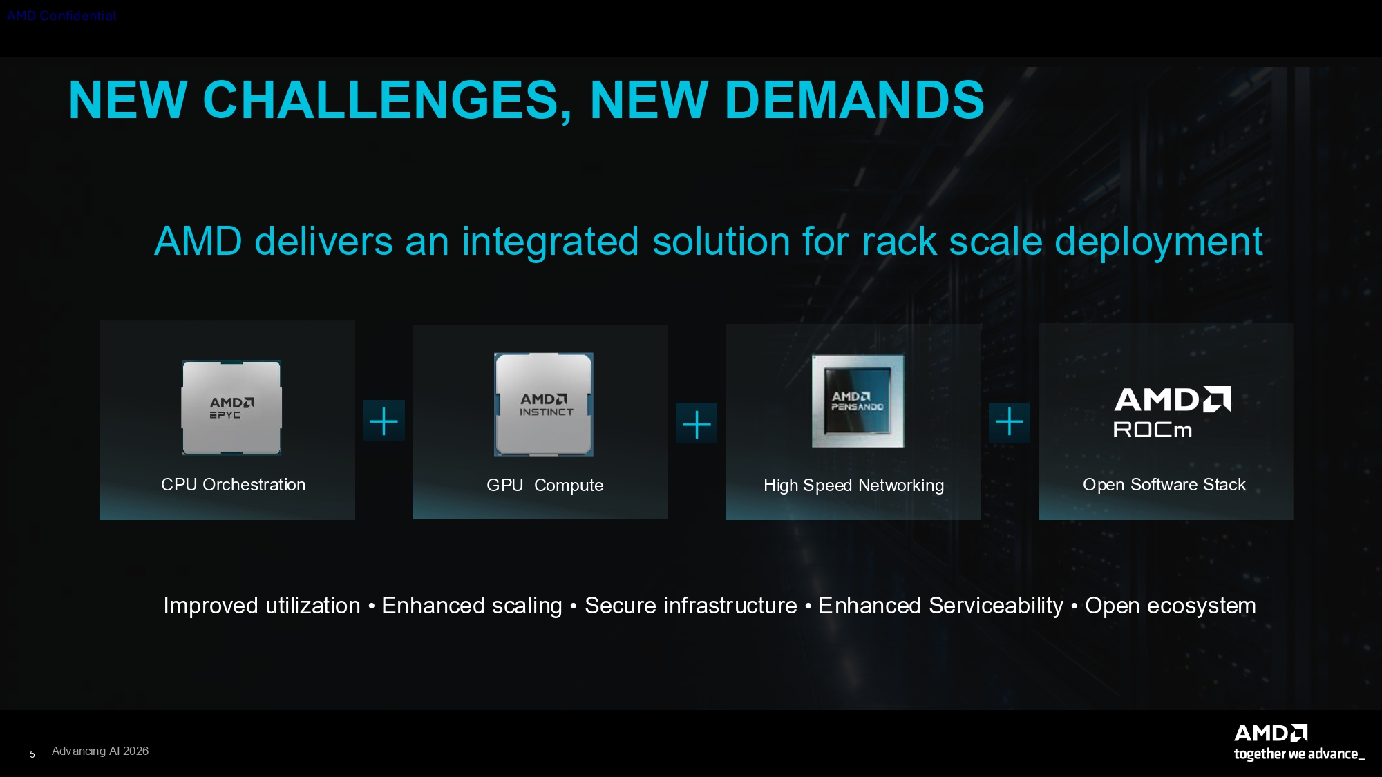
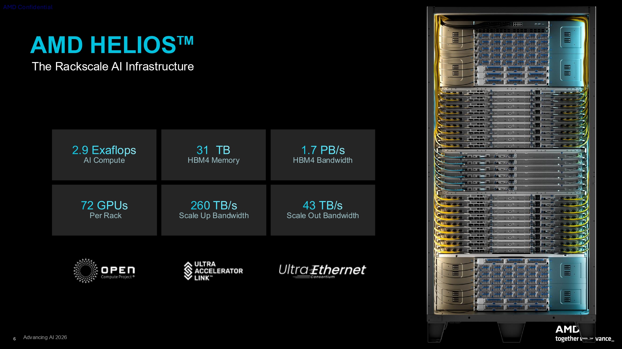
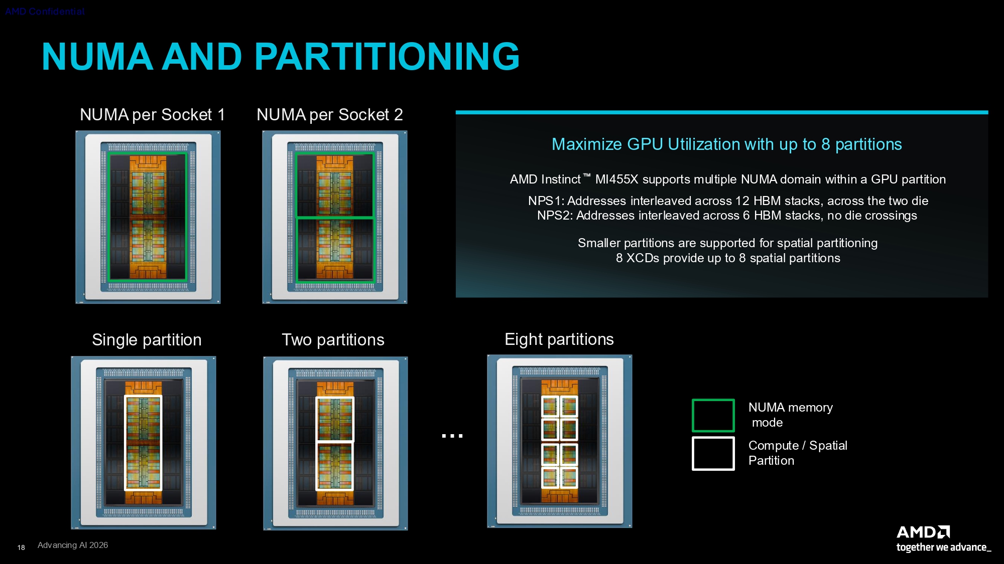
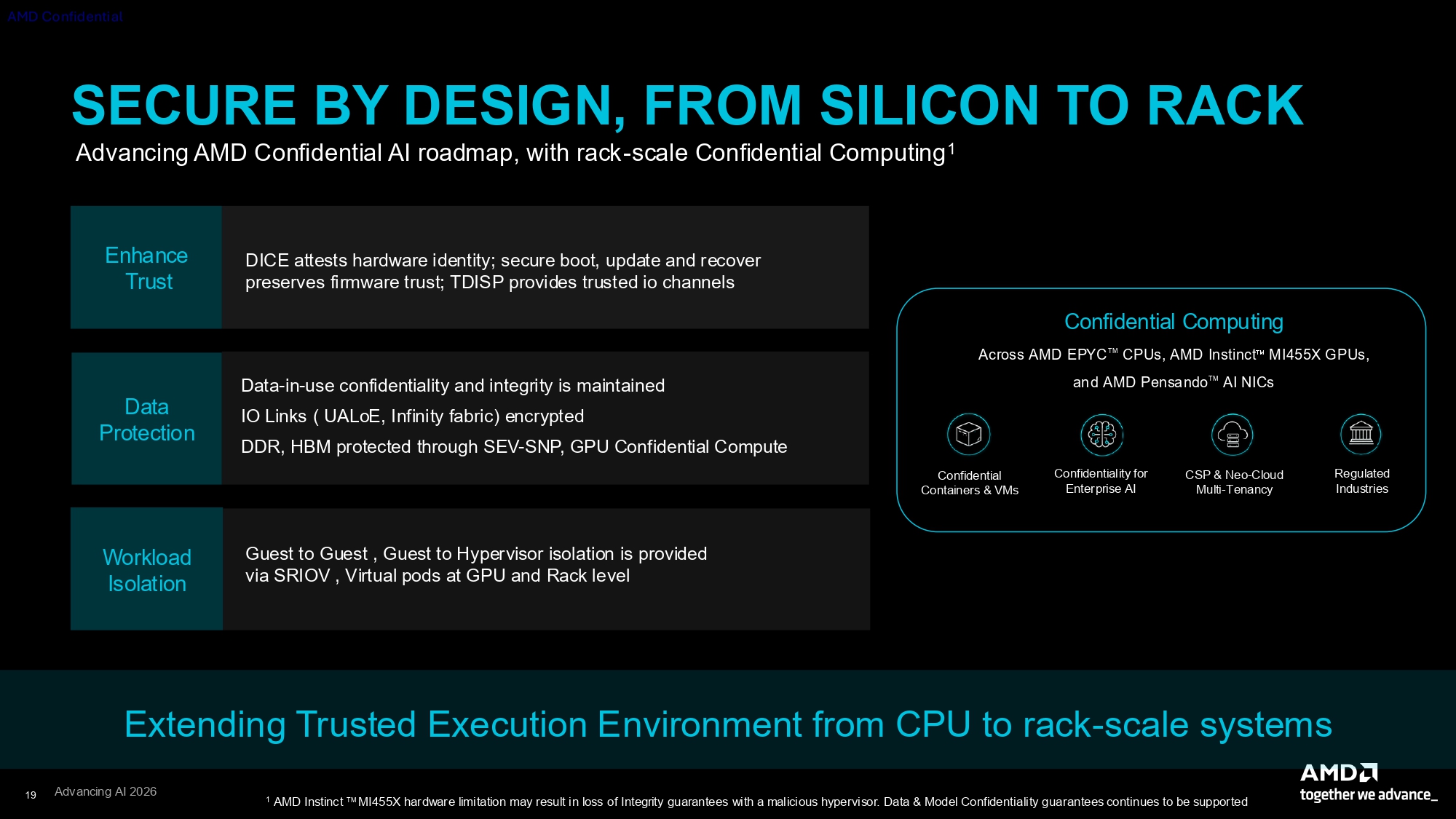
At AMD’s Advancing AI event this week, the company revealed more details of its upcoming MI455X GPU and the Helios rack-scale architecture that will join 72 of those GPUs into a coherent accelerator—the largest such system that AMD has built so far and its first to truly compete with Nvidia’s NVL72 rack-scale design, as used in the Blackwell and Rubin generations.
AMD calls the MI455X “by leaps and bounds the most advanced AI accelerator we’ve ever built,” and from what we’ve seen, it’s the most competitive product at both the chip level and at rack scale that AMD has ever put up against Nvidia’s thorough dominance of the AI compute race.
(Image credit: AMD)
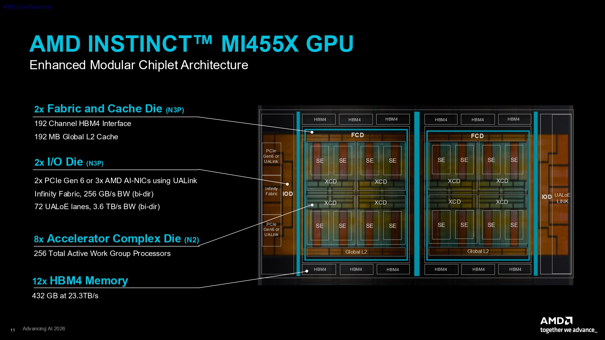
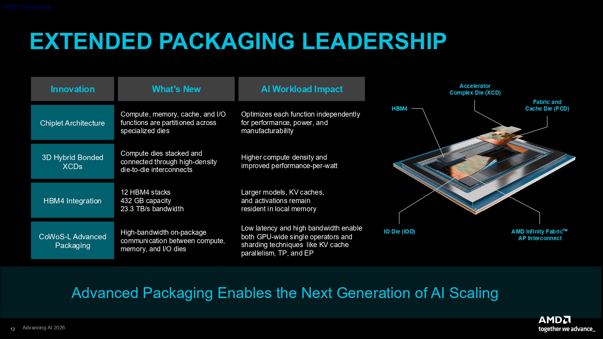
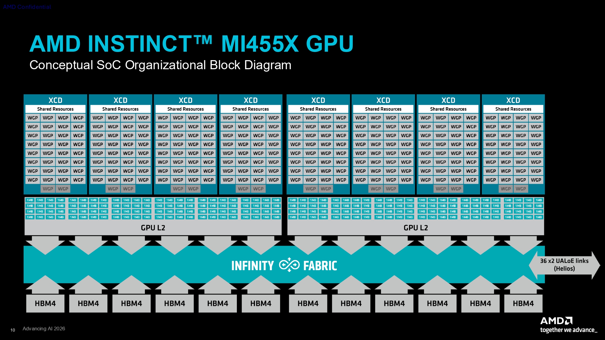
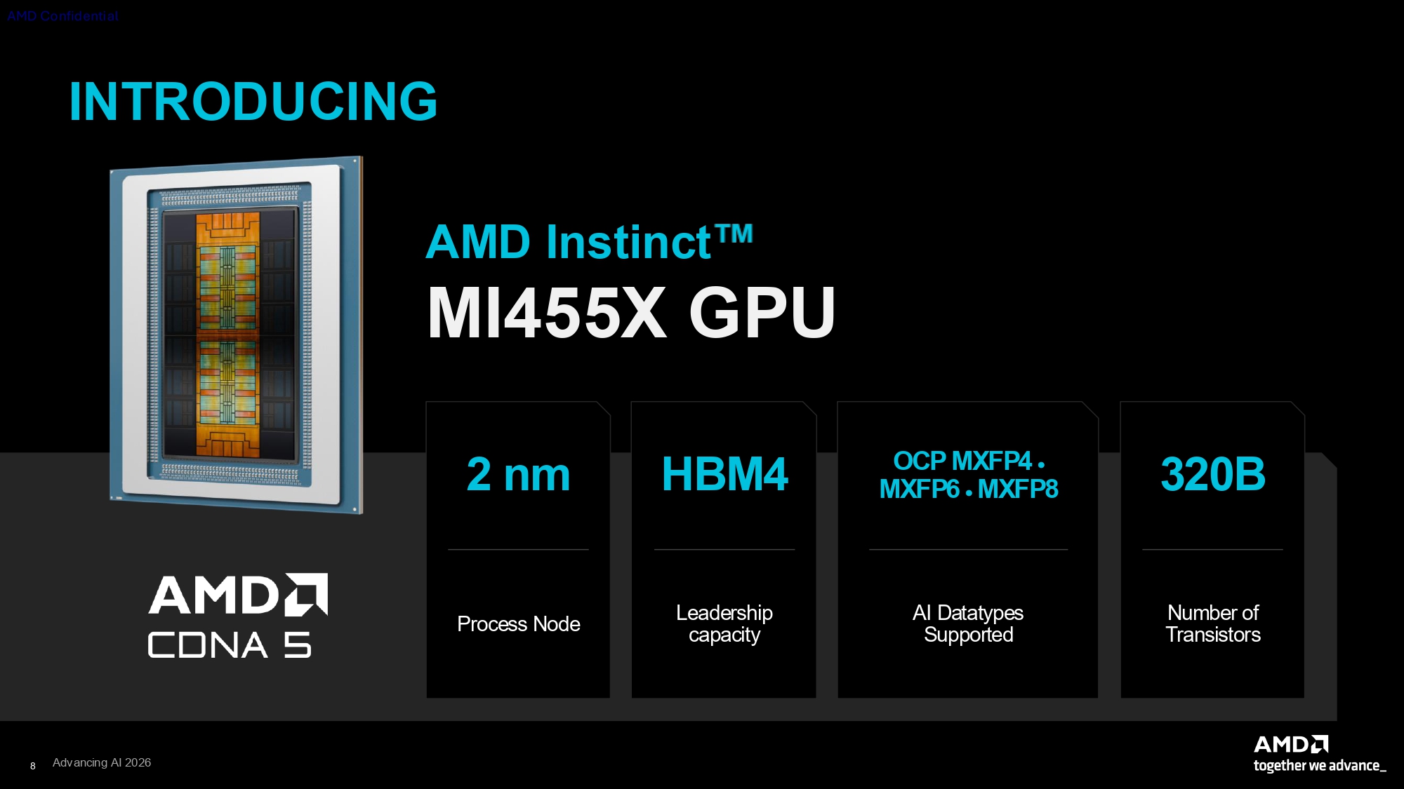
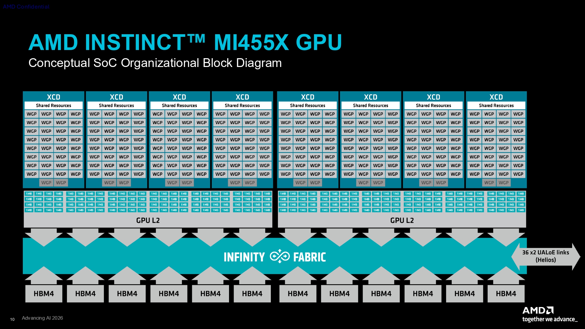
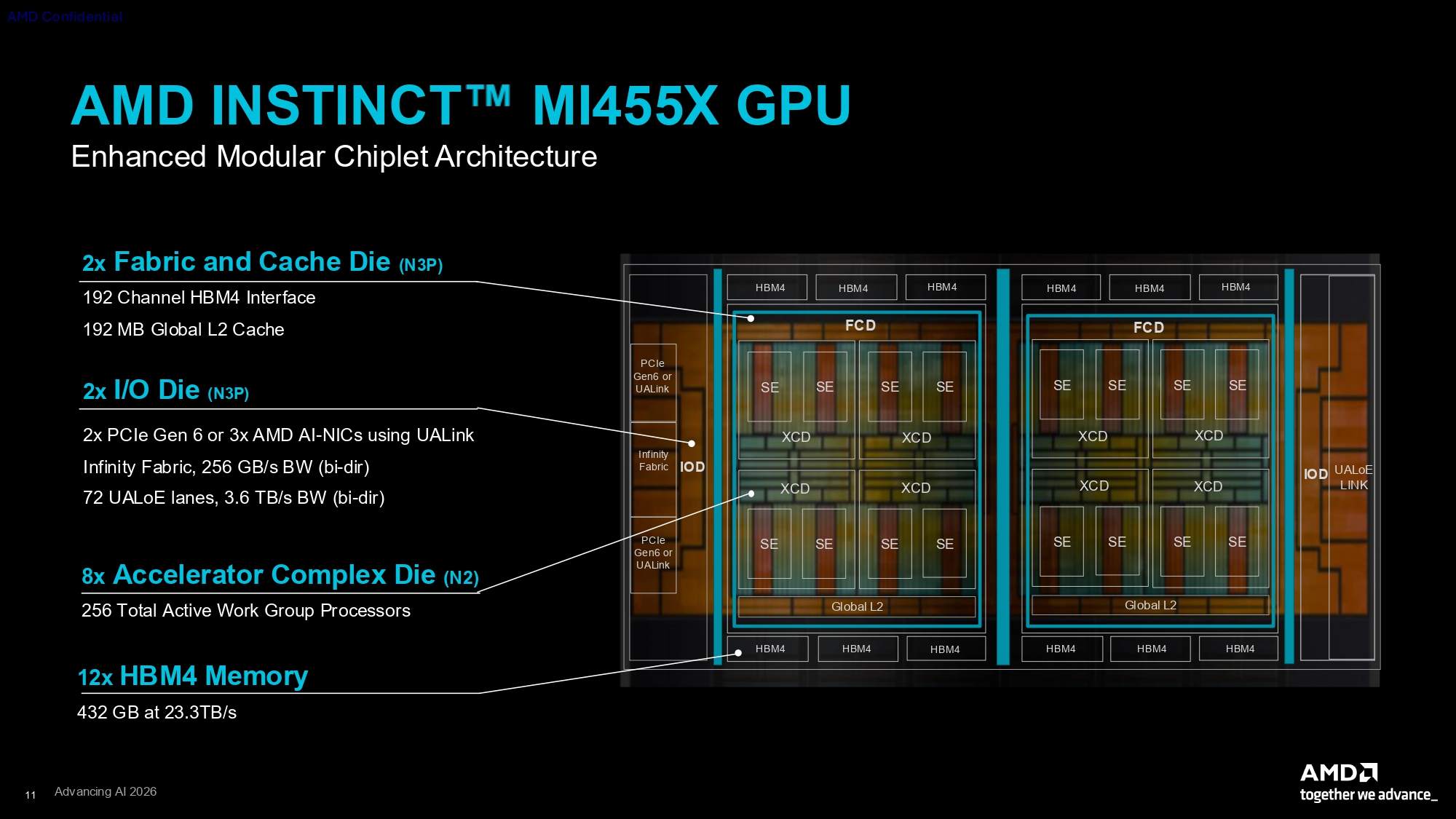
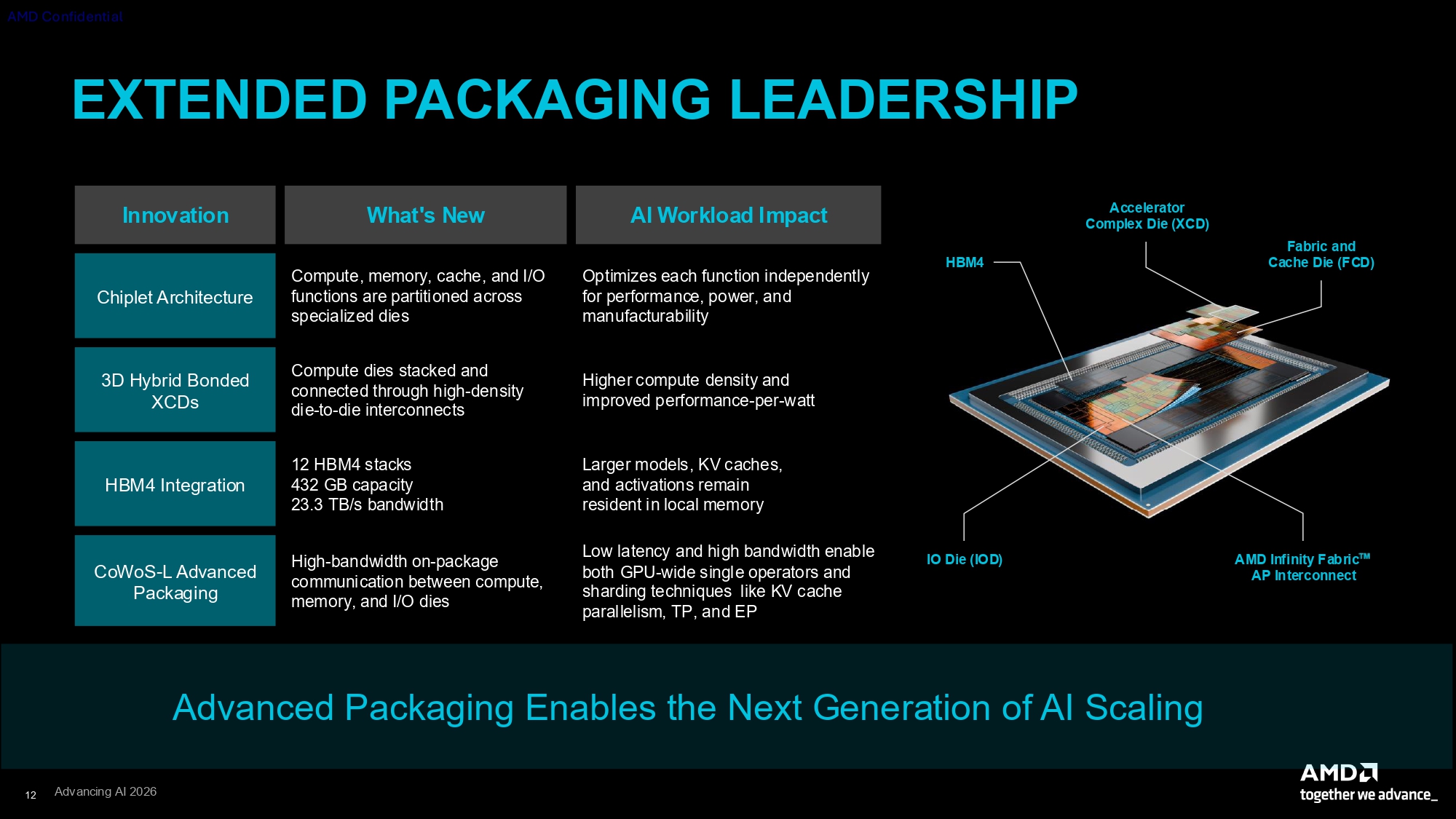
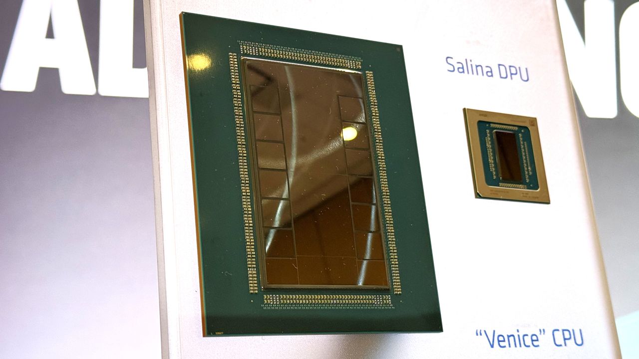
The full MI455X GPU is a massive chip encompassing 320 billion transistors, and it’s built up using advanced packaging technologies. Four Accelerator Complex Dies (XCDs) are stacked on top of each Fabric and Cache Die (FCD) using hybrid bonding. In turn, the two FCDs are each joined to six stacks of HBM4, the two I/O dies, and to one another using TSMC’s CoWoS-L technology.
(Image credit: AMD)
This chiplet design lets AMD use the most advanced TSMC 2N gate-all-around (GAA) process technology on the XCDs, where it’s most beneficial for power and performance, while the FCDs and I/O dies, which contain elements that don’t benefit from the densest process technologies, are fabricated on TSMC N3P.
CDNA 5 represents a large shift in the shape of the CDNA architecture. AMD now calls the fundamental building block of the CDNA 5 Accelerator Complex Die a “Work Group Processor” instead of a “Compute Unit,” but in practice, the basic layout of the rest of the Accelerated Complex Die (XCD) is largely similar.
(Image credit: AMD)
The number of WGPs on the MI455X remains the same as on the MI355X at 256. Because there hasn’t been a change to the number of fundamental compute resources on the chip, the per-WGP throughput on the CDNA 5 MI455X has to be much higher than on the MI355X to deliver its large performance boost.
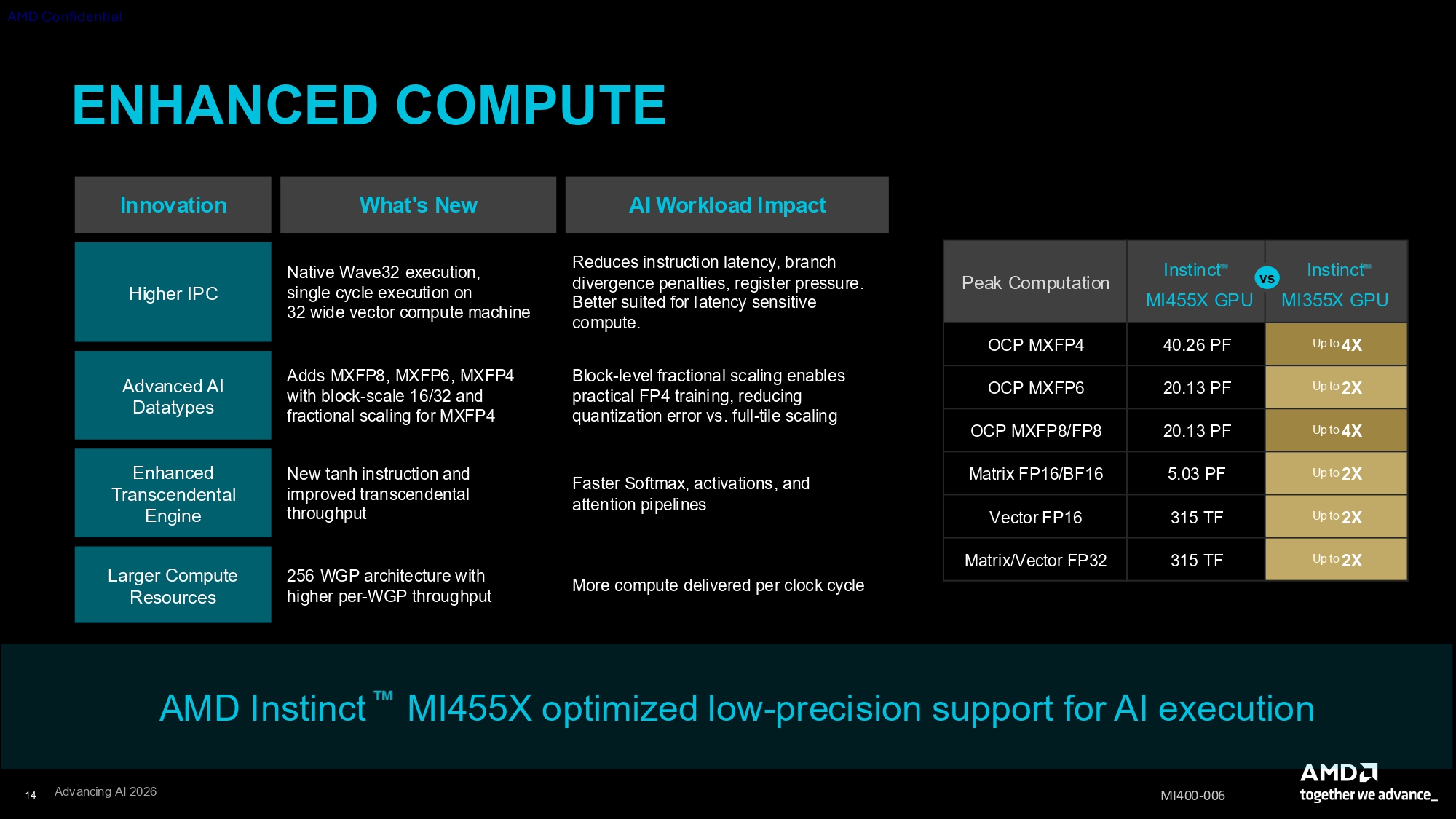
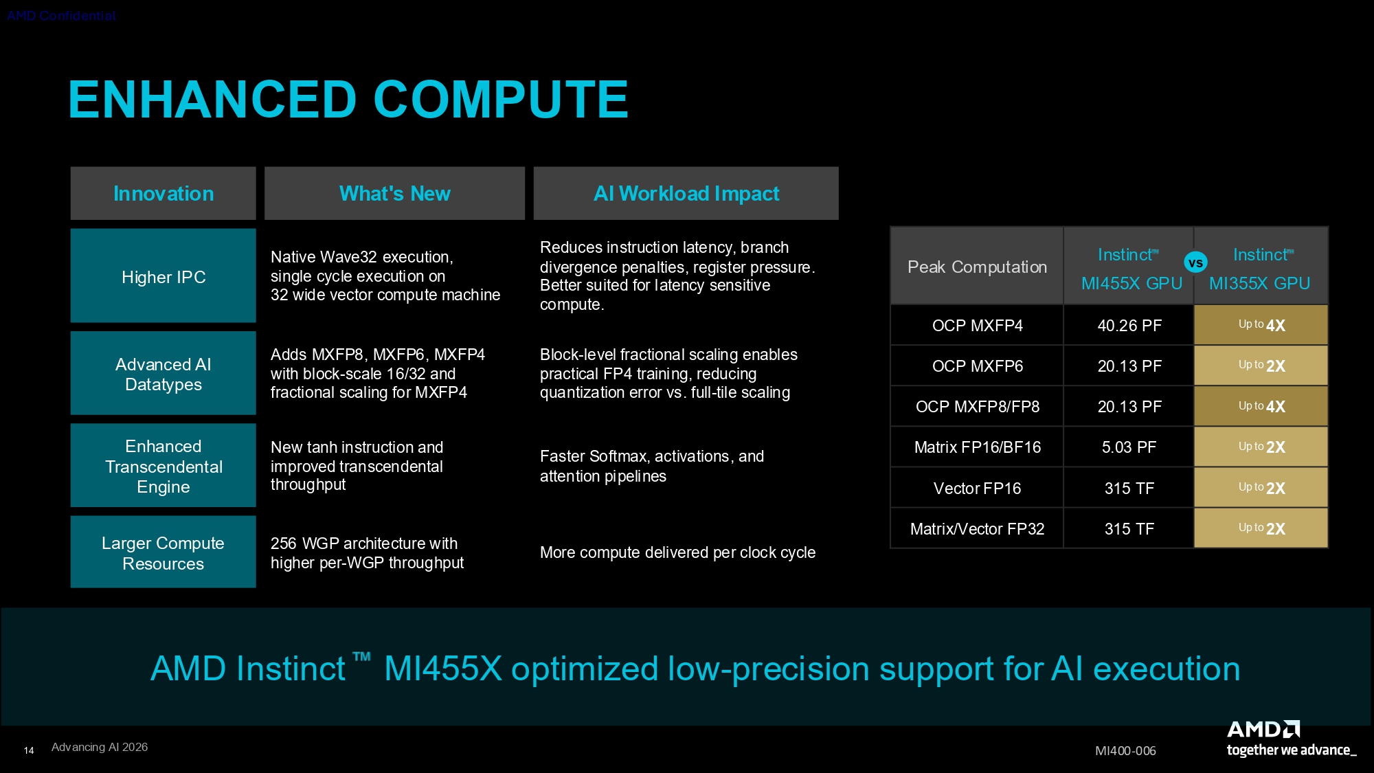
Among the many other changes for this generation, CDNA 5 marks a major shift for the programming model of an Instinct GPU. The width of a wavefront, or group of work items or threads that each workgroup processor addresses, is now 32 instead of 64, a choice AMD says improves instruction latency, branch divergence penalties, and register pressure. It further explains that a 32-wide approach increases the flexibility of the architecture for interacting with different tensor tile sizes and mapping compute kernels to the hardware. RDNA GPUs have used a native wavefront size of 32 since their introduction.
(Image credit: AMD)
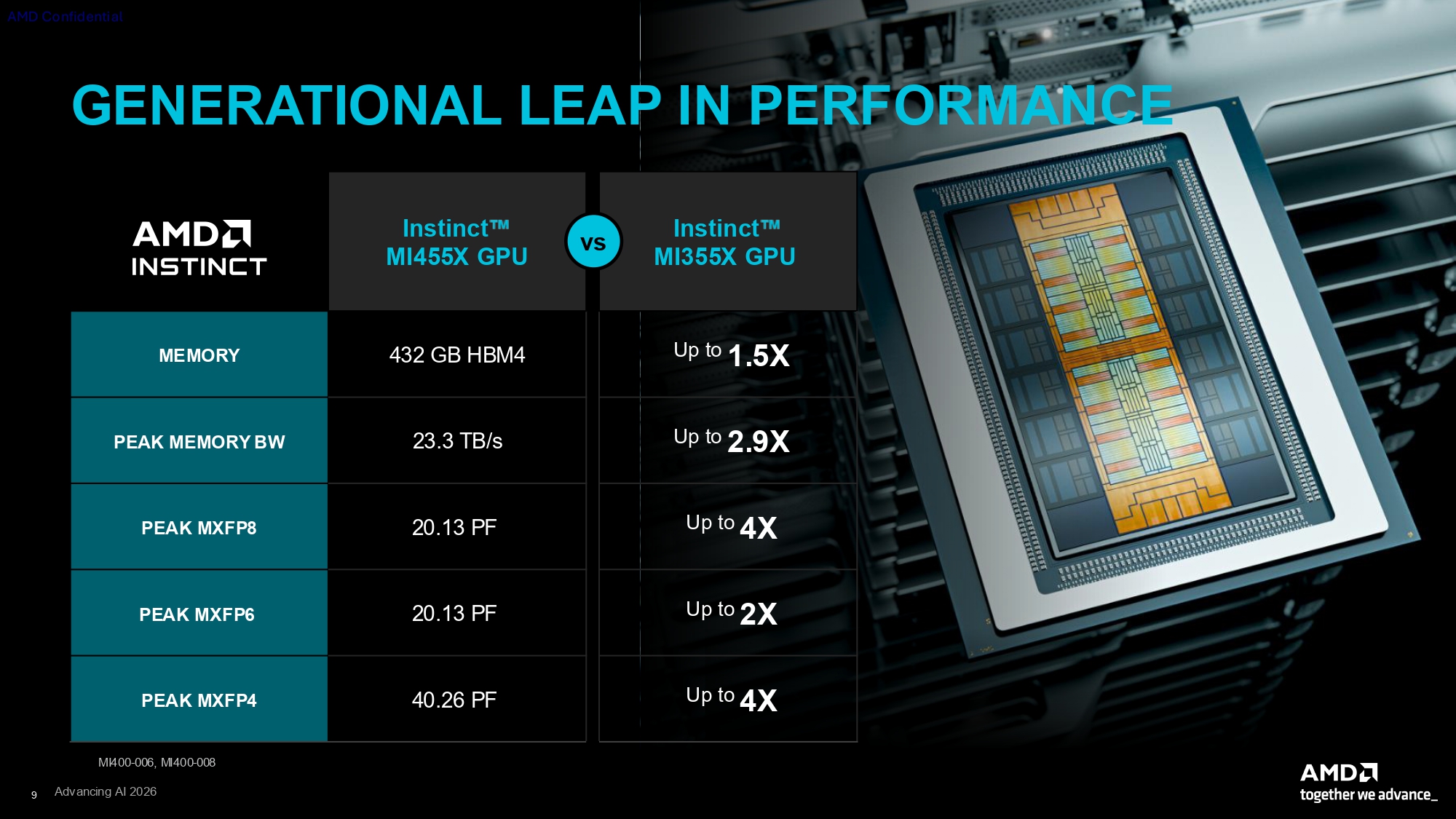
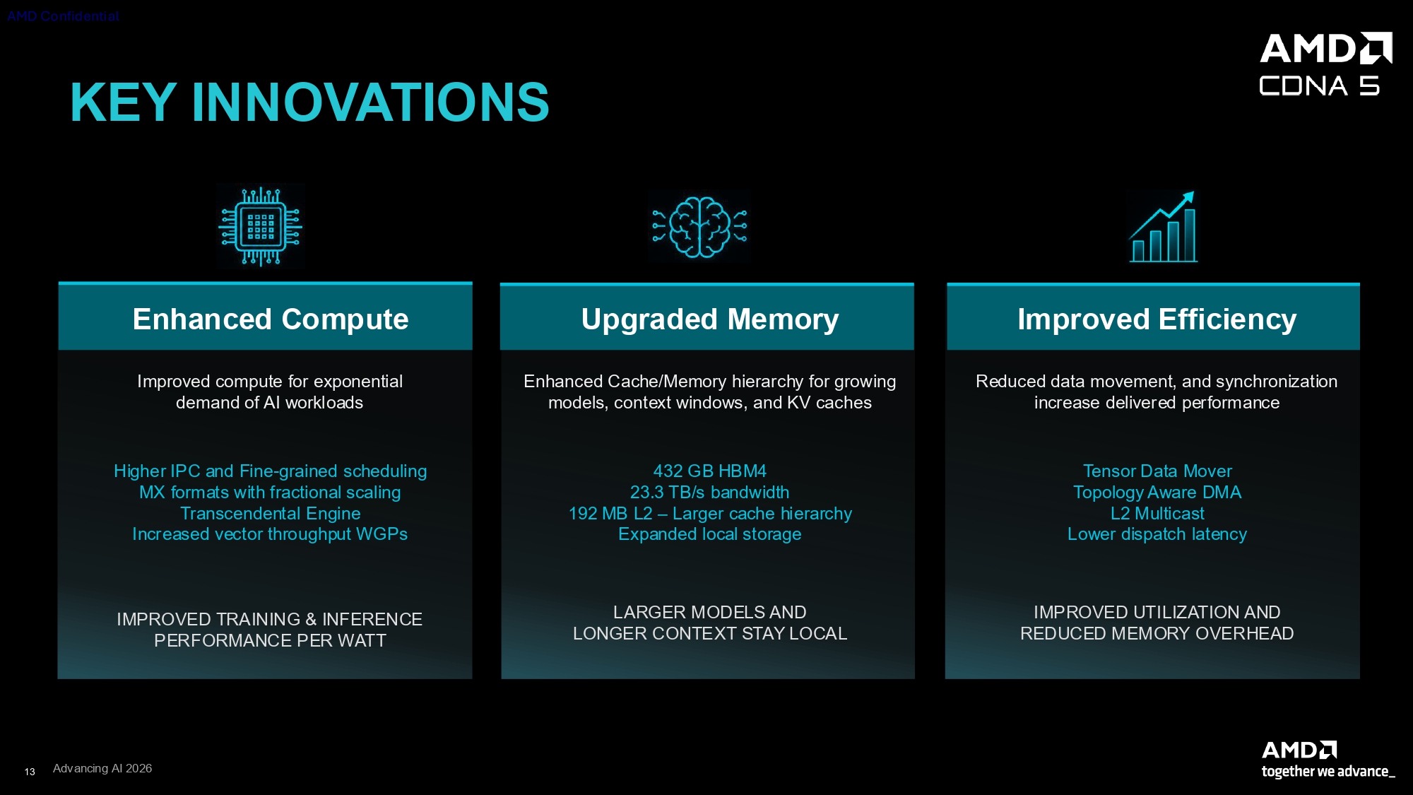
CDNA 5 greatly enhances compute performance over CDNA 4, theoretically doubling and in some cases quadrupling the peak FLOPS possible from the chip. The MI455X especially benefits lower-precision floating-point formats now common for use in inference. OCP MXFP8 and MXFP4 formats are theoretically up to 4X faster than on the CDNA 4 MI355X.
Here’s an overview of the MI455X’s theoretical peak FLOPS compared to both the previous-generation MI355X and Nvidia’s Rubin GPU.
AMD Instinct MI455X Peak FLOPS
Instinct MI355X
Instinct MI455X
Nvidia Rubin
NVFP4 (dense)
--
--
35 PF
OCP MXFP4
10 PF
40.26 PF
--
OCP MXFP6
10 PF
20.13 PF
17.5 PF
OCP MXFP8
10 PF
20.13 PF
17.5 PF
Matrix FP16/BF16
2.5 PF
5.03 PF
4 PF
Vector FP16
157.3 TF
315 TF
--
Matrix FP32
157.3 TF
315 TF
400 TF
Vector FP32
157.3 TF
315 TF
130 TF
At least on paper, the MI455X offers peak performance that bests what Nvidia has shown for Rubin so far, and in combination with the Helios rack-scale architecture that finally gives AMD the same 72-GPU coherent domain as Nvidia’s NVL72 rack-scale design, AMD is more competitive in the AI data center capacity race than ever before. And that’s translating into real customer wins, as AMD has announced pivotal deals with Microsoft and Anthropic this week.
But we’d be careful about drawing too many conclusions from these head-to-head peak FLOPS numbers, as the realized performance of these GPUs in the real world is likely to be much lower in practice, as AMD itself admitted in one of our sessions. The ongoing challenge will be to optimize software and applications to achieve as much of that theoretical performance as is possible.
Beyond its general compute improvements, AMD is also touting improved transcendental math performance from the CDNA 5 Transcendental Unit, which has wide-reaching implications for performance on essential AI functions like softmax, neural network activations, and attention. AMD says that the CDNA 5 Transcendental Unit doubles throughput versus CDNA 4. The Transcendental Unit also adds support for an explicit tanh instruction, which is useful for certain operations on hidden layers within neural networks.
(Image credit: AMD)
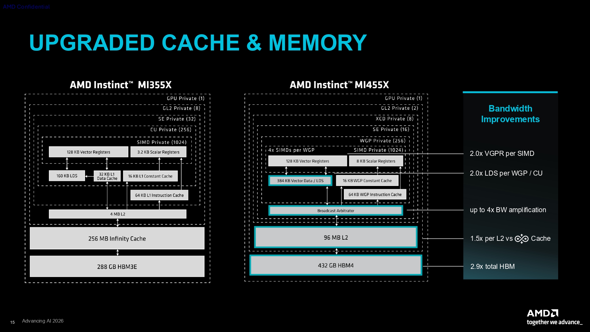
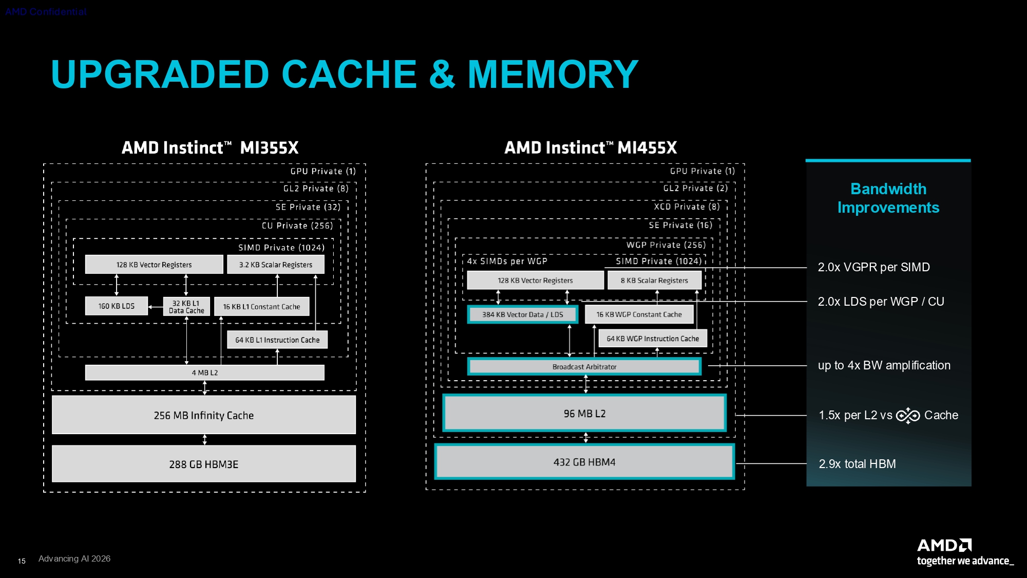
AMD also deeply revised the cache and memory hierarchy on the MI455X. The large Infinity Cache on CDNA 4 has been ditched in favor of a smaller but higher-bandwidth shared L2 cache on each Fabric Compute Die. Each FCD has a 96MB L2 slice for 192MB in total, compared to just 32MB backed by the 256MB Infinity Cache on the MI355X. AMD says this cache offers 1.5X higher bandwidth per FCD compared to the CDNA 4 Infinity Cache, so in aggregate, the MI455X has 3X the L2 bandwidth compared to the MI355X.
Within the WGP, larger, faster, and more flexible caches are now available. The local data store (LDS) or scratchpad memory has doubled in size versus CDNA 4, to 320 KB, and in total, there is 96 MB of LDS across the chip, twice that of the largest CDNA 4 implementation on the MI355X. AMD says the LDS SRAM offers higher read and write bandwidth per clock than in the previous generation, but it didn’t provide specifics.
Critically, the main memory architecture of MI455X has moved to HBM4 for this generation. AMD uses six stacks of HBM4 per FCD for a total of 12 on the chip, offering a memory capacity of 432GB and memory bandwidth of 23.3 TB/s per GPU. High memory capacity and bandwidth are both crucial for keeping ever-expanding AI model weights and KV caches close to the GPU for the best performance.
This HBM implementation is one of the MI455X’s strongest advantages over Nvidia’s Rubin in isolation. It offers both much higher capacity and slightly higher bandwidth than the first Rubin GPU that Nvidia detailed this week. In its initial configuration, Rubin only offers 288GB of HBM4 with up to 22 TB/s of bandwidth.
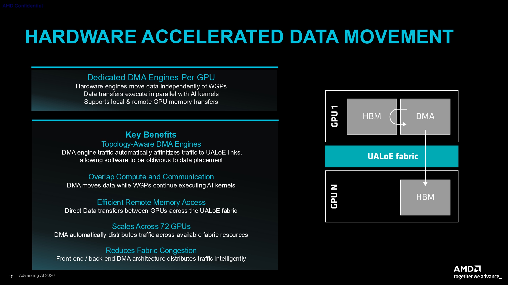
At rack scale, the MI455X’s higher HBM capacity adds up to 31.1 TB of HBM across 72 GPUs, or a whopping 50% more than the 20.7 TB aggregate capacity of Vera Rubin. And the Helios rack-scale architecture is AMD’s first to join all of that GPU memory into a single coherent domain. Since AI inference performance is dominated by both data locality and memory bandwidth, AMD’s advantages in this regard are sure to attract plenty of attention.
AMDAMD
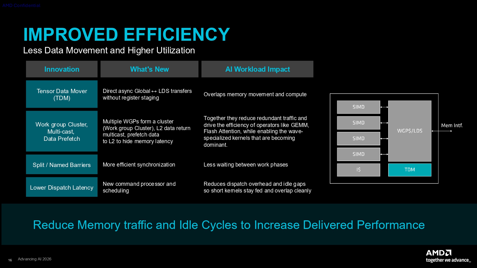
Efficient data movement across the chip is a key consideration for reducing power consumption and improving performance on the MI455X.
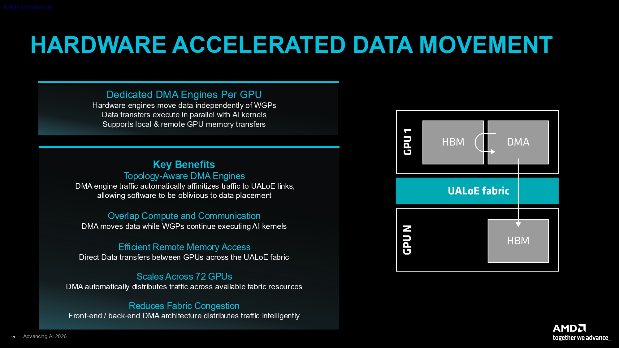
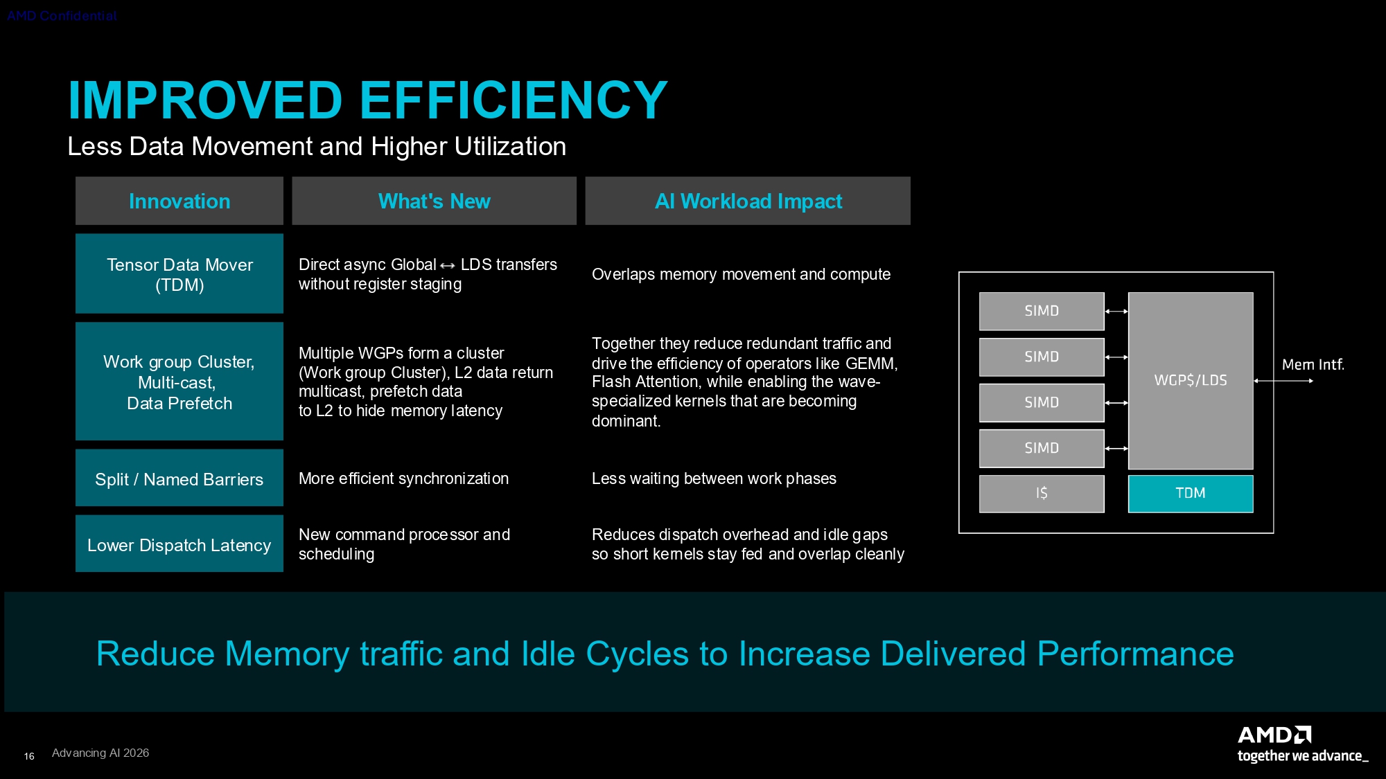
The CDNA 5 Tensor Data Mover is an improved version of the data movement engine in past CDNA generations. Like Nvidia’s Tensor Memory Accelerator, the TDM accelerates the production of certain tensor-specific memory addresses and facilitates moving the related data from memory without involving the shader engines. In the CDNA 5 generation, the TDM gains the ability to move data directly from DRAM to the WGP LDS cache without staging data at intermediate cache levels.
AMD has also added multicast support for memory reads to the WGPs to take advantage of the fact that AI workloads often need to work on the same weights and activations across multiple WGPs at once. By using multicast, a single memory read can be amplified across many WGPs, increasing effective memory bandwidth, reducing duplicated traffic on the bus, and lowering power consumption. Nvidia has had a similar capability in its GPUs since Hopper, but given AMD’s intense focus on efficient data movement this generation, it’s perhaps unsurprising to see a version of it added here.
All told, the MI455X is AMD’s most compelling Instinct product yet. It delivers a massive generational performance improvement, it puts up peak FLOPS on paper that are competitive with or even superior to Nvidia’s upcoming Rubin GPU, and it offers a massive 432GB pool of HBM4 memory that’s 1.5x larger and even slightly faster than Rubin’s 288GB complement.
Combined with the Helios rack-scale architecture and its 72-accelerator scale-up domain—AMD’s first true answer to Nvidia’s NVL72 rack-scale design—we should expect the race for AI compute superiority to really heat up in the second half of this year as both Nvidia and AMD begin delivering their next-generation products to customers.
The GeForce RTX 3090 may no longer be one of the best graphics cards. However, it can still compete with the top performers today with a little help from its younger sibling, the GeForce RTX 3050. Recently, a resourceful gaming enthusiast who goes by the name quziwuzzi explained on Reddit that they paired these two Ampere-based graphics cards and used LosslessScaling technology to dramatically boost their combined performance, achieving up to 144 FPS at 4K (3840x2160) resolution.
Lossless Scaling is a very powerful yet affordable tool on Steam that costs just $7 and brings AI upscaling and frame generation to the masses. What differentiates Lossless Scaling from proprietary solutions, such as Nvidia DLSS, AMD FSR, or Intel XeSS, is its wide compatibility with any game or video software. It works seamlessly regardless of whether the title or application comes with official support for these proprietary solutions.
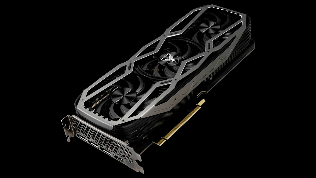
In this example, the Gainward GeForce RTX 3090 Phoenix takes on the primary workload of running and rendering the game. Meanwhile, Lossless Scaling handles the demanding frame generation duties. But instead of stealing resources from the primary GPU, it operates on a secondary graphics card, the Asus Dual GeForce RTX 3050 OC Edition. The setup allows the GeForce RTX 3090 to focus exclusively on rendering the game by offloading the frame generation process to the GeForce RTX 3050.
According to the Redditor who shared their experience, the GeForce RTX 3090 delivered up to 71 FPS at a 4K resolution. When paired with the GeForce RTX 3050 and using Lossless Scaling for frame generation, the system's performance doubled and reached 144 FPS at 4K. The author did not mention which games were used for testing. The motivation for the uplift was to take advantage of the Redditor's 42-inch LG C4 OLED television, which features a 144 Hz refresh rate.
Lossless Scaling supports 2X, 3X, and 4X frame generation multipliers that essentially duplicate, triplicate, or quadruplicate the perceived frame rate. While the technology is compatible even with iGPUs, you logically need the right discrete graphics card to get the best results. The GeForce RTX 3050 proved more than sufficient for handling frame generation at 4K resolution. According to the Redditor's firsthand account, Lossless Scaling’s 2X, 3X, and adaptive modes all worked fine.
The global memory shortage is still in full force and continues to put immense pressure on the availability and pricing of graphics cards. The cost of upgrading to the latest and greatest graphics card is out of reach for many gamers. As a result, the gaming community is constantly looking for affordable solutions to boost performance without throwing the house out the window. Lossless Scaling tool can breathe new life into your existing hardware. If you are lucky enough to have a spare graphics card lying around, you can put it to good use. Even something as old as the GeForce GTX 750 Ti or Radeon RX 550 can improve your system's gaming performance.
Some may argue that frame generation is fake frames. But for only $7, it is a cost-effective way to trick your brain for the meantime and improve the gaming experience, at least until the memory shortage subsides and you can upgrade your graphics card for real.
When Microsoft and Qualcomm launched the first Copilot+ PCs sporting Snapdragon X Elite processors, the CPU performance was beyond reproach, but whether due to immature software or underwhelming integrated hardware, the GPU horsepower left a lot to be desired. The easiest way to solve that is to hook up a discrete GPU, of course, but nobody's managed that yet. Instead, an enterprising hacker in China has become the first person to publicly get an Nvidia GeForce RTX GPU running on an Arm-based platform using Windows 11, but it's not Snapdragon, and it's not an Nvidia CPU, either, WindowsLatest reports.
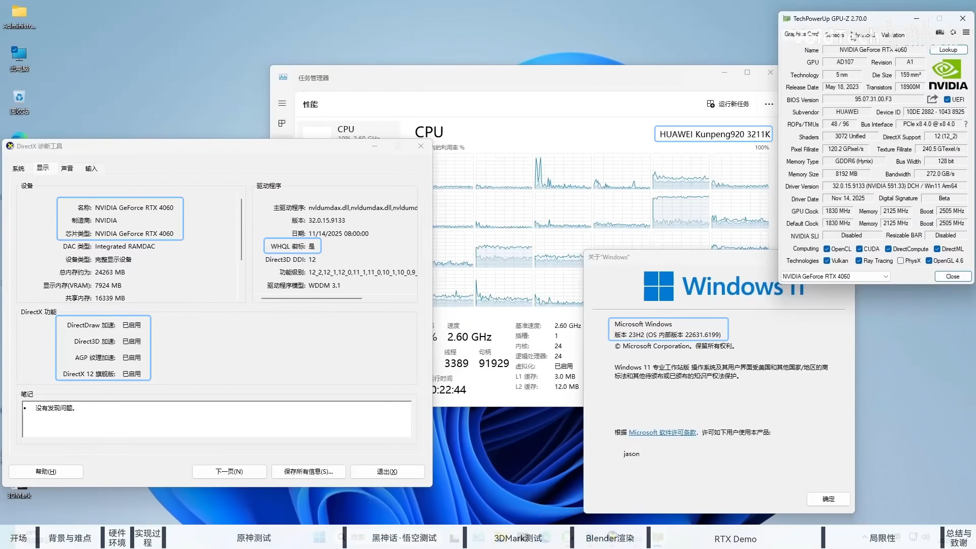
We knew that the Nvidia RTX Spark processors used an integrated GPU directly derived from Nvidia's Blackwell technology, and we also knew that those machines would run Arm Windows 11, so this was bound to happen sooner or later, because that necessarily means that there is an Nvidia client graphics driver for Arm-based Windows 11 out there. That's exactly what "VoidTech" on BiliBili used for his experiment, though the experiment wasn't without some pitfalls.
(Image credit: VoidTech / BiliBili)
Specifically, VoidTech got an Nvidia GeForce RTX 4060 8GB graphics card working in a Huawei Qingyun W510 workstation. This machine does not have a Snapdragon processor, of course; Huawei makes its own CPUs, and indeed this chip is the Kunpeng 920, created by Huawei's HiSilicon division. This chip was considered a major milestone when it was introduced in 2019, as it's a 7nm server CPU with up to 80 cores, although the specific implementation in the Qingyun W510 has "only" 24 cores.
All those cores don't help it much in gaming. As PC gamers will be well aware, CPU gaming performance is basically down to single-threaded CPU performance and system memory latency. The custom TaiShan v110 cores in the Kunpeng 920 only offer up around a sixth of the single-core performance of something like a Ryzen 9 9700X, at least going by Passmark, with the usual caveats that apply to Passmark. Combined with relatively small caches and a DDR4 memory interface that's clearly tuned for throughput, not latency, and you have a recipe for middling gaming performance. That's before we even start talking about x86 emulation penalties.
Benchmark Comparison
Qingyun W510 + GeForce RTX 4060 8GB
Ryzen 7 5800X + GeForce RTX 4060 8GB
Passmark ST / MT
733 / 9496
3448 / 27671
Genshin Impact 1080p High
~25 FPS
= 60 FPS (cap)
Black Myth Wukong 1080p Medium
21 FPS
83 FPS
3DMark Speed Way
2252
2682
3DMark Time Spy Graphics
6369
10939
3DMark Time Spy CPU
3402
10775
3DMark Night Raid GPU
43530
61080
3DMark Solar Bay
32373
49435
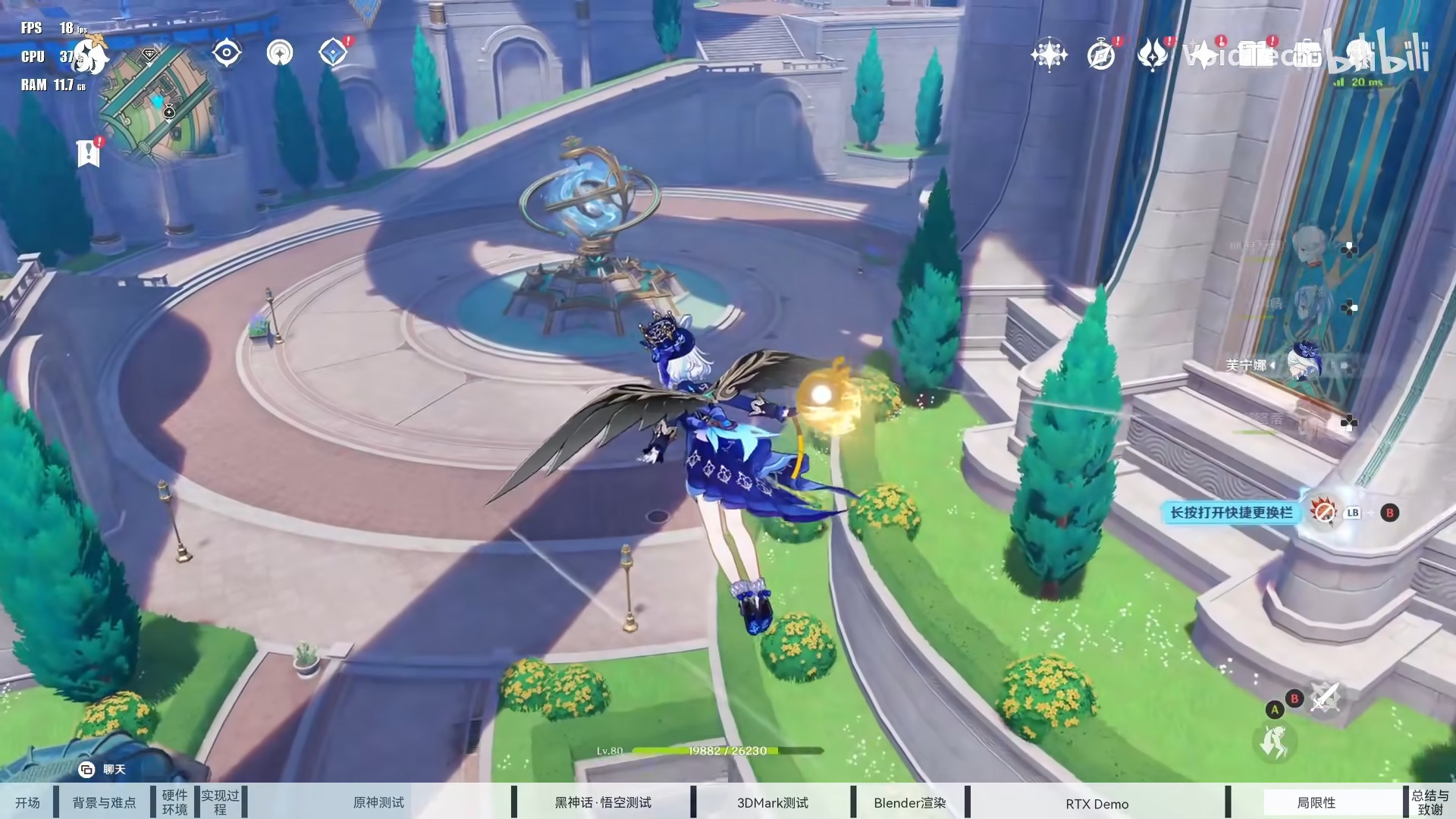
So did it work? Well, more or less. Actually, the GeForce RTX 4060 did about half of its job flawlessly, running advanced games like the Unreal Engine 5-based Black Myth Wukong and slightly less advanced games (Genshin Impact), as well as various 3DMark tests. Most software seemed to work without any issues aside from overall weak performance due to the slow Kunpeng 920 CPU; the Wukong benchmark finished at 21 FPS, while Genshin Impact struggled to break 25 FPS and stuttered frequently. However, Arknights: Endfield refused to launch, likely due to an incompatibility between its restrictive "Anti-Cheat Expert" package and the Prism translation layer required to run the x86 Windows games on Arm Windows.
While the performance in Genshin Impact isn't great—your smartphone probably runs it better—it's sort of impressive that it runs at all. (Image credit: VoidTech / BiliBili)
The half of its job that the RTX 4060 didn't do was that VoidTech wasn't actually able to get a video signal out of the graphics card. He notes that the graphics card was recognized, and the monitor was picked up, too. He simply couldn't get the system to properly push pixels to the monitor. This likely comes down to the Nvidia Arm driver being built specifically for the RTX Spark and thus missing the necessary code to support the HDMI and DisplayPort encoders on desktop graphics cards. To get around this issue, VoidTech used the Sunshine game streaming server and the Moonlight game streaming client (on another system) to run the Huawei machine headlessly. A janky solution to be sure, but it does seem to have worked.
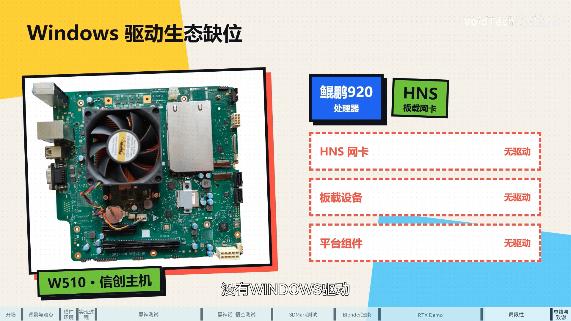
Because the workstation was meant for Linux, there are no Windows drivers for the network controller or other integrated devices, including audio. (Image credit: VoidTech / BiliBili)
There's a bit more to the video, including how VoidTech had a hard time getting Windows 11 to boot on the machine at all due to broken ACPI tables, some frustration with missing Windows 11 drivers for the HiSilicon Network Subsystem (HNS), a bit where he runs a Blender Cycles render on the GeForce RTX 4060, and a couple of Nvidia RTX demos including the Star Wars "Reflections" demo that was shown with the introduction of the RTX 20 Series "Turing" GPUs. It's an interesting saga of making hardware that was never meant to work together run on an operating system that none of it supports.
This does somewhat bode well for RTX Spark. While you probably shouldn't expect the Cortex-X925 CPU cores in the RTX Spark to outpace the latest AMD or Intel CPUs due to still being forced to pay the Prism penalty, they're going to be a damn sight faster than this seven-year-old workstation chip. Since the drivers seem to be in good shape, the consumer laptops should indeed offer capable gaming performance when they arrive later this year—at least, as long as your game doesn't have kernel-level anti-cheat
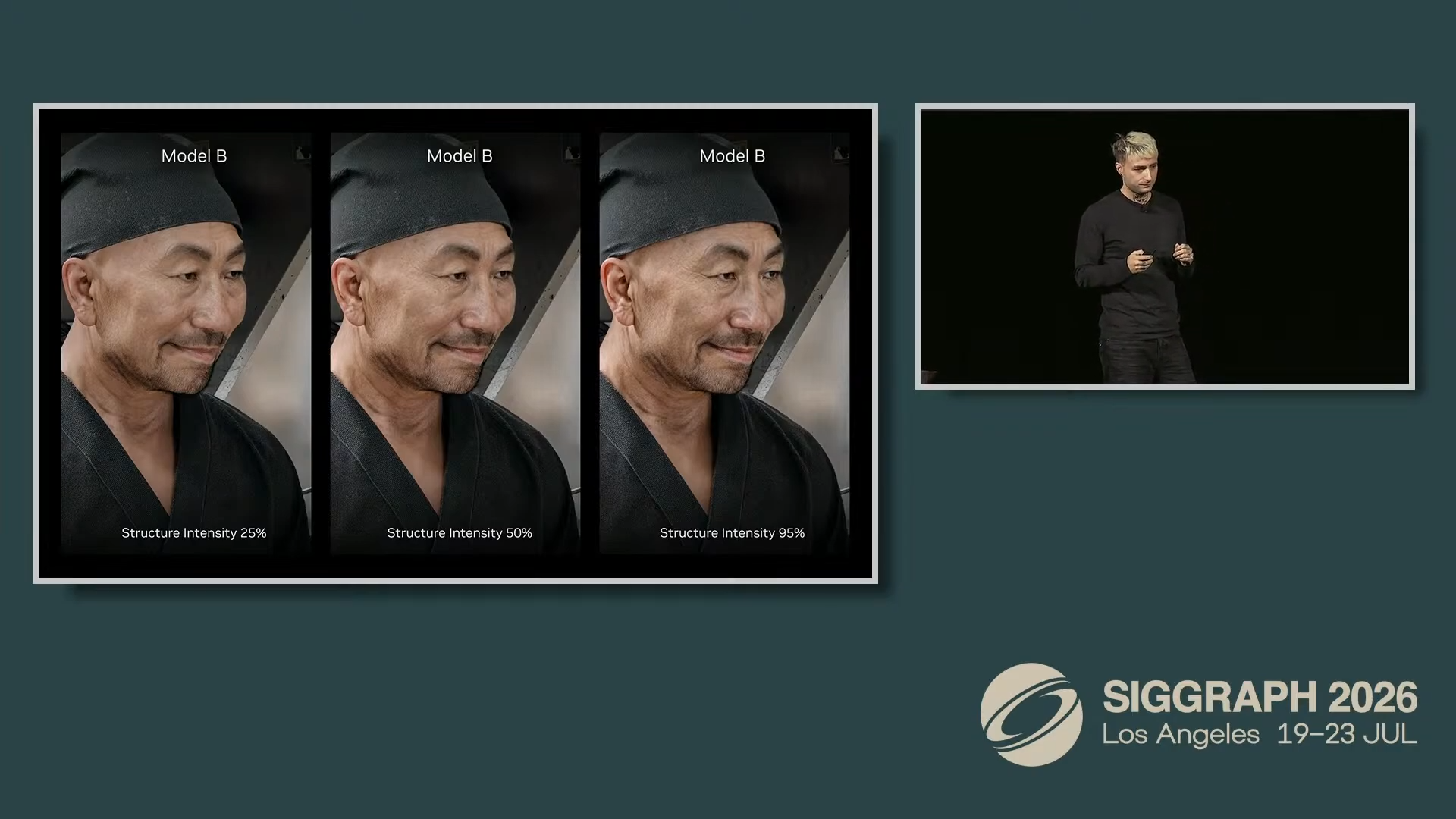
Nvidia first debuted DLSS 5 earlier this year to a strong, critical response. The upscaling tech was almost slammed by some press and enthusiasts for overstepping its boundaries and going too far with AI.
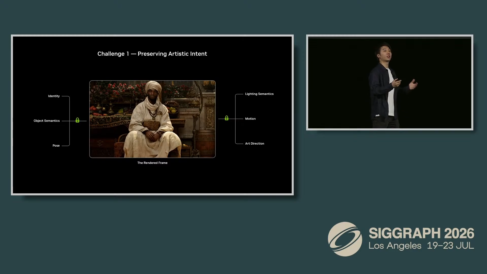
At the time, Nvidia reassured the community that DLSS 5 would preserve artistic intent and CEO Jensen Huang even went as far as to claim that gamers didn't understand it. Now, at SIGGRAPH, the company has once again showcased DLSS 5, and it admittedly looks different this time around.
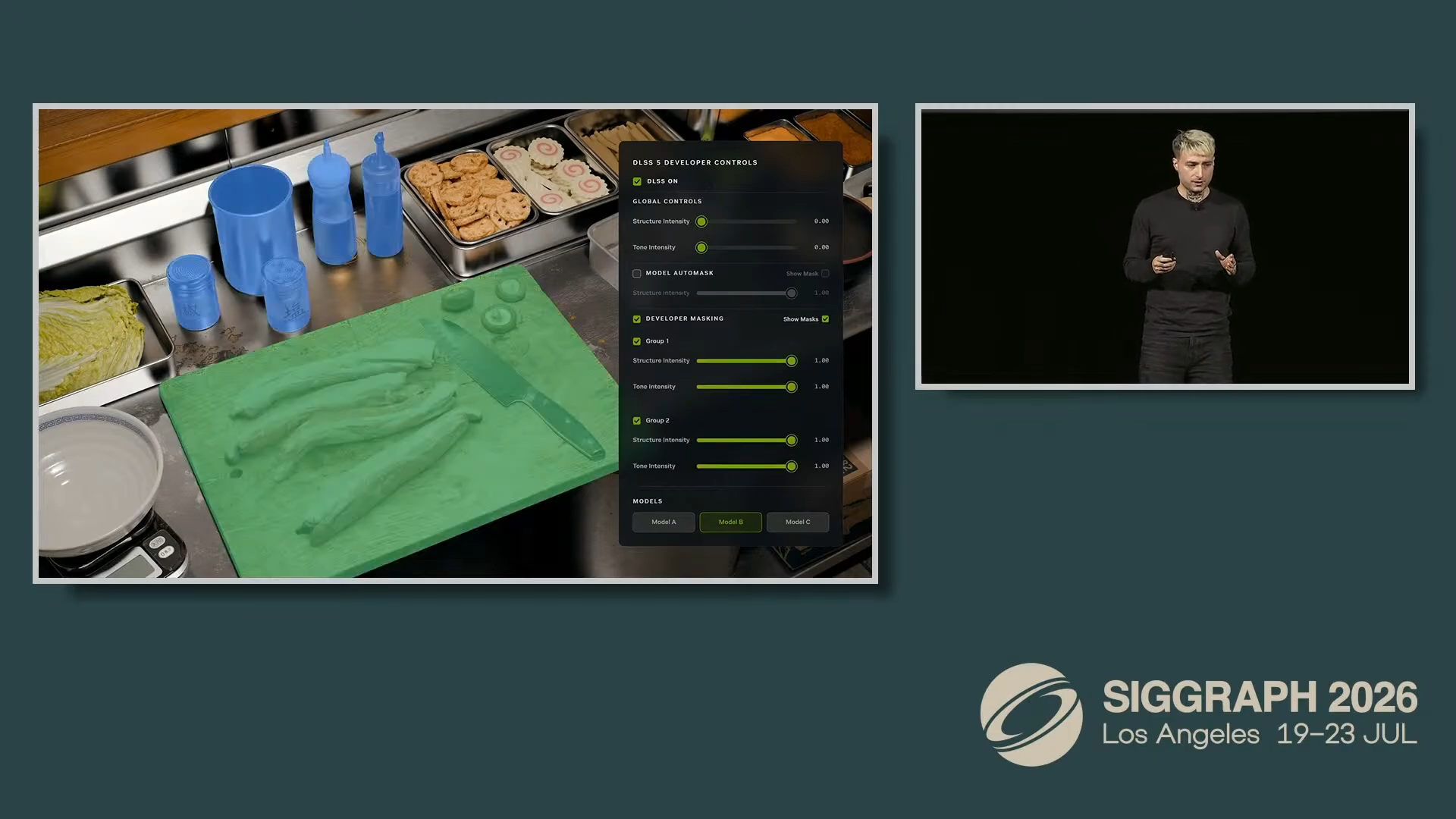
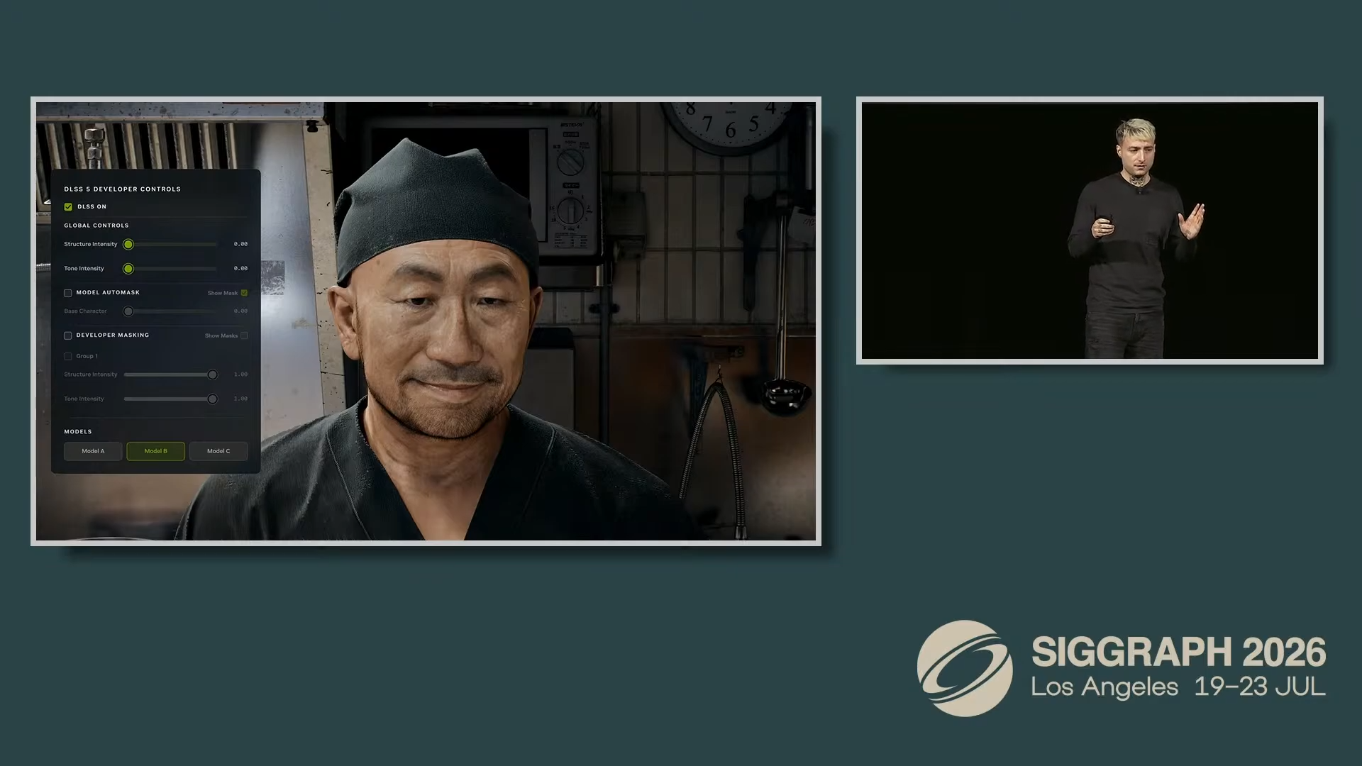
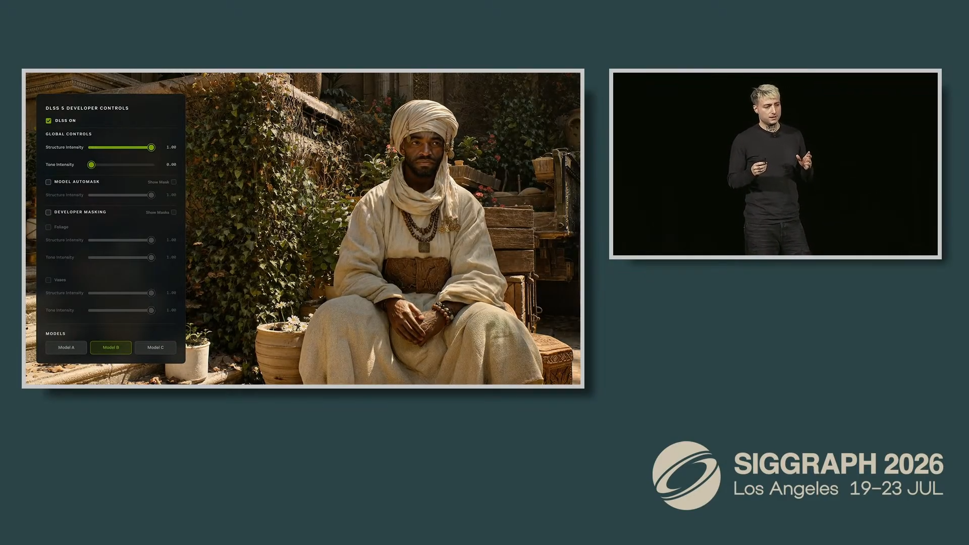
The main takeaway is the introduction of three different models with varying levels of detail and impact on performance. A game doesn't need to be confined to a single model the whole time; instead, developers can choose to employ different models for different scenes. Individual elements of scene, such as the characters versus the world, can also be fine-tuned in respect to how much DLSS touches them up (or not at all).
Nvidia Nvidia
Then, you have the liberty to switch between the models in real time without incurring latency. DLSS 5 uses a combination of techniques to take the original rendered frame and apply effects on top, going beyond just upscaling the image. These days, DLSS, FSR, and XeSS are mandatory parts of the equation, acting as the preferred anti-aliasing solution in modern titles, and helping in other areas like ray tracing.
The upscaling part works conventionally and is still responsible for dictating the foundational blocks of the image, like lighting and geometry. The part that was so heavily criticized is therefore optional, as it only comes into play after the original rendered frame has been upscaled. However, it's unclear whether developers (or you) can actively choose to not process the frame through the beautification features.
Nvidia Nvidia
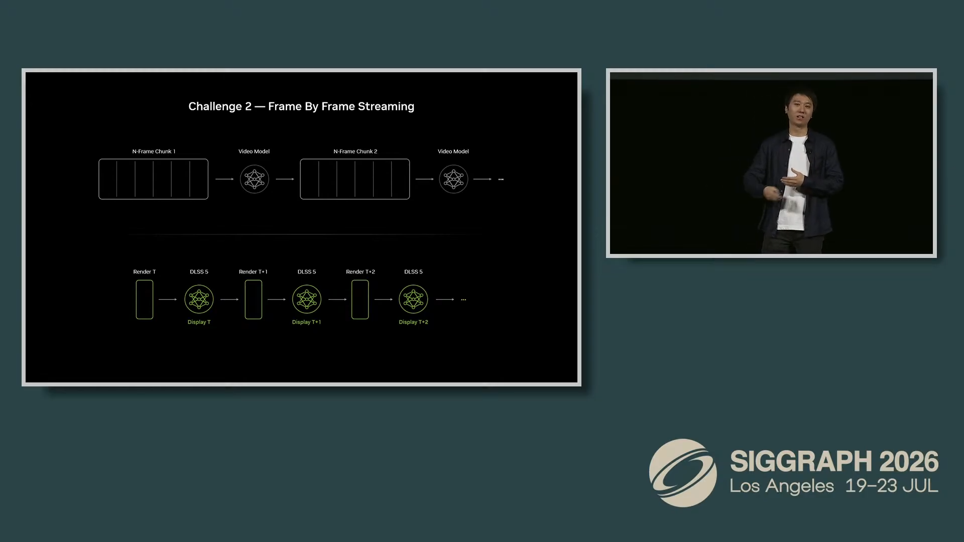
Nvidia outlined three main challenges that the company faced when developing DLSS 5, some of which is probably reactionary after the initial reveal. The first challenge is preserving the original creative vision, which we already explained. The second challenge was to handle one frame at a time, which generative AI models don't — they process multiple frames together. That means DLSS 5 shouldn't negatively affect response times.
Nvidia Nvidia Nvidia
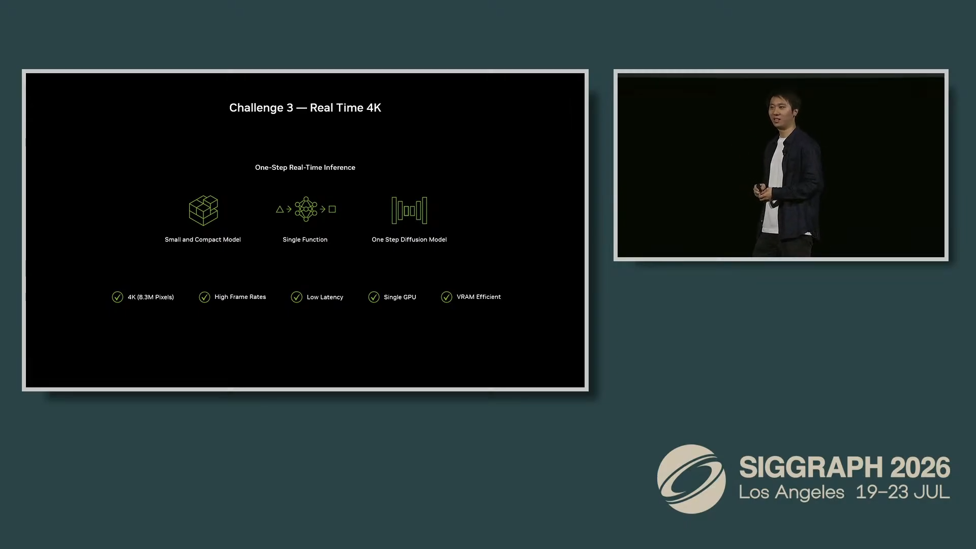
The third and final challenge pertains to the optimization of DLSS 5. The slides shown at SIGGRAPH say the model can run on a single GPU and that it's "VRAM efficient." For context, last time we saw it running on two RTX 5090s. Nvidia did not say whether it still needs the highest-end Blackwell gaming GPU to work properly. The company is promising real-time 4K performance thanks to a more compact model that has learned from a larger diffusion model.
DLSS 5 is building up to be a significant step for upscaling tech just when we thought AMD was finally catching up. However, many people may still worry about artistic intent, even if the new demos look a lot more polished and mature. We'll have to see what happens when it finally releases. There is no official release date for DLSS 5, but it should launch during Q3 2026 as Nvidia continues to tweak the models and its parameters based on community feedback.
Nvidia's upcoming Vera Rubin platform, set to arrive later this year, will take the stage as the AI world shifts towards an era dominated not by frontier training runs but by the demands of agentic AI inference at massive scale. The hunger for generated tokens in agentic workflows and the demands of delivering them quickly, efficiently, and at low unit cost now dominate the discussion.
We’ve already gone in depth on new performance data around the Vera CPU and how it helps to accelerate agentic AI workloads, but that’s not all Nvidia is sharing today. It’s also detailing some new features of the Rubin architecture and how those features are meant to increase inference efficiency from the GPU level to rack-scale and data-center-scale implementations of this accelerator platform.
(Image credit: Nvidia)
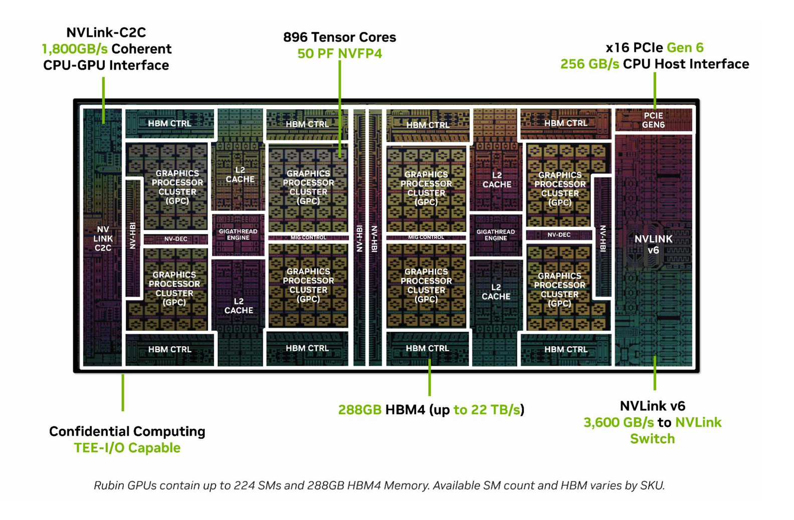
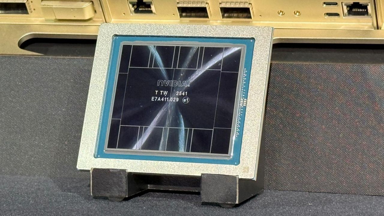
The full Vera Rubin NVL72 rack-scale system is built up from 36 Vera CPUs and 72 Rubin GPUs, but our focus today is on the GPU proper. Rubin joins two compute dies onto a single package using the Nvidia High Bandwidth Interface. The resulting chip offers 224 Streaming Multiprocessors (SMs) containing a total of 896 Tensor Cores alongside 288GB of HBM4 memory providing 22 TB/s of memory bandwidth.
As an inference-focused accelerator, Nvidia touts Rubin’s 50 sparse PFLOPS of NVFP4 inference throughput as its headline performance figure, although that’s only one of a dizzying array of data types this chip can handle. Here are some key rates to keep in mind for this chip so far:
Nvidia Rubin GPU
NVFP4 Inference
50 PFLOPS (with sparsity)
NVFP4 Training
35 PFLOPS
FP8/FP6 Training
17.5 PFLOPS
INT8
250 TOPS
FP16/BF16
4 PFLOPS
TF32
2 PFLOPS
FP32
130 TFLOPS
FP64
33 TFLOPS
Let’s dive into some of Rubin’s refinements for inference workloads to understand how Nvidia aims to keep all of those resources fully utilized.
The Rubin Tensor Memory Accelerator efficiently manages growing MoE models
First up, Nvidia highlights efficiency improvements in the Tensor Memory Accelerator (TMA) that help feed the Tensor Cores with data. The TMA is a dedicated engine built to handle memory address calculations and perform direct loads of array data into a GPU's shared local memory.
Leading AI model architectures have moved from dense models where every parameter is activated per output token to a mixture-of-experts (MoE) architecture where only certain specialized sub-networks are activated per token, based on the guidance of a router that helps judge which experts are best suited to processing a given input.
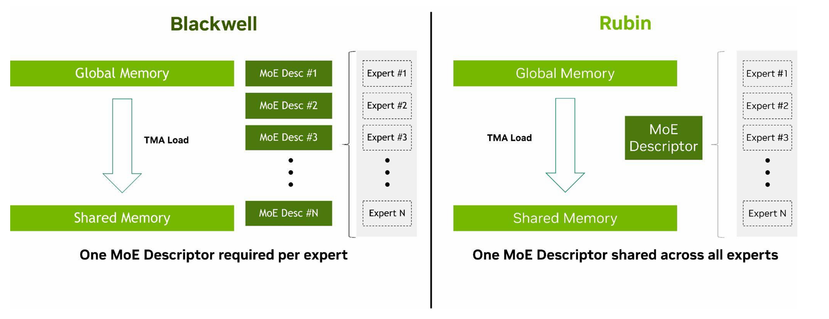
MoE expert weights can be distributed across GPUs in order to efficiently utilize limited per-GPU HBM capacity. Nvidia says that Rubin's TMA has been improved to deal with the challenges of managing the growing numbers of experts in today’s leading models.
(Image credit: Nvidia)
The TMA in Blackwell GPUs needed to maintain separate MoE descriptors in memory for the location of every expert, meaning that the overhead of locating and moving those expert weights requires more compute resources as the number of experts grows.
The Rubin TMA now supports GPU kernels that maintain and update a single unified MoE descriptor directly in the TMA instruction at runtime, reducing computation of MoE descriptor metadata and requiring less calculation overhead for data movement. This approach frees up GPU cycles for inference calculations, which is, of course, the place that you want your expensive AI accelerator spending the vast majority of its time.
Doubled K-dimension throughput, double the Tensor Core output
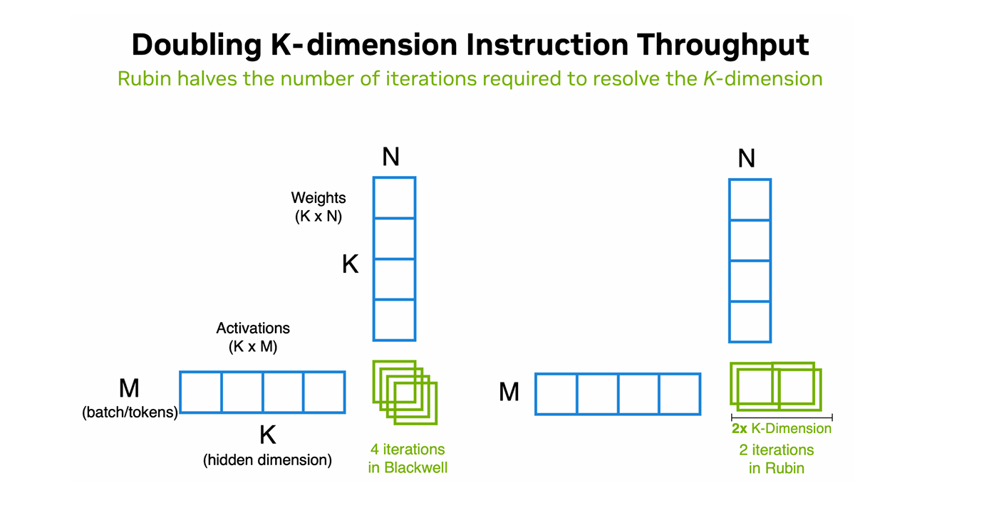
Rubin also improves the fundamental performance of matrix operations in the Tensor Core by doubling the amount of work those cores can perform on the K dimension, or the shared inner dimension of a pair of matrices to be multiplied. Without going too deep into the math, the size of the K dimension is directly related to the number of times the Tensor Core has to loop over the elements of the two matrices being multiplied.
(Image credit: Nvidia)
In Nvidia's example, then, the calculation of a result matrix that would require four loop iterations on Blackwell can be completed in only two on Rubin. Nvidia says this improvement has wide-ranging benefits for throughput-, memory-, and latency-bound kernels, and it’s helpful for both context processing and decode phases of inference.
Softmax on Rubin gets up to a 4X boost versus Blackwell
Rubin also focuses on improving the performance of the attention mechanism that’s foundational to transformer-based LLMs More advanced models now support context lengths of up to a million tokens, and quickly performing attention calculations on such long input sequences quickly is a key driver for improved inference performance.
Softmax is an essential operation in attention calculations, and in order to keep up with the improved Tensor Core throughput in Rubin, Nvidia has once again boosted softmax throughput in the GPU SM’s Special Function Unit (SFU).
Since it relies on the transcendental math capabilities of the SFU, softmax throughput can become a bottleneck for subsequent inference work, and it's a limitation that Nvidia already sought to address with enhancements to the Blackwell Ultra SFU. Blackwell Ultra doubled FP32 and BF16/FP16 exponential throughput compared to the first-gen Blackwell GB200.
GPU
FP32 Exponential Throughput
BF16/FP16 Exponential Throughput
Blackwell
1x
1x
Blackwell Ultra
2x
2x
Rubin
2x
4x
Rubin maintains Blackwell Ultra's 2X speedup over Blackwell in FP32 exponential math, and it doubles BF16/FP16 exponential calculations again compared to Blackwell Ultra, leading to a 4X improvement in throughput compared to Blackwell for those lower-precision data types.
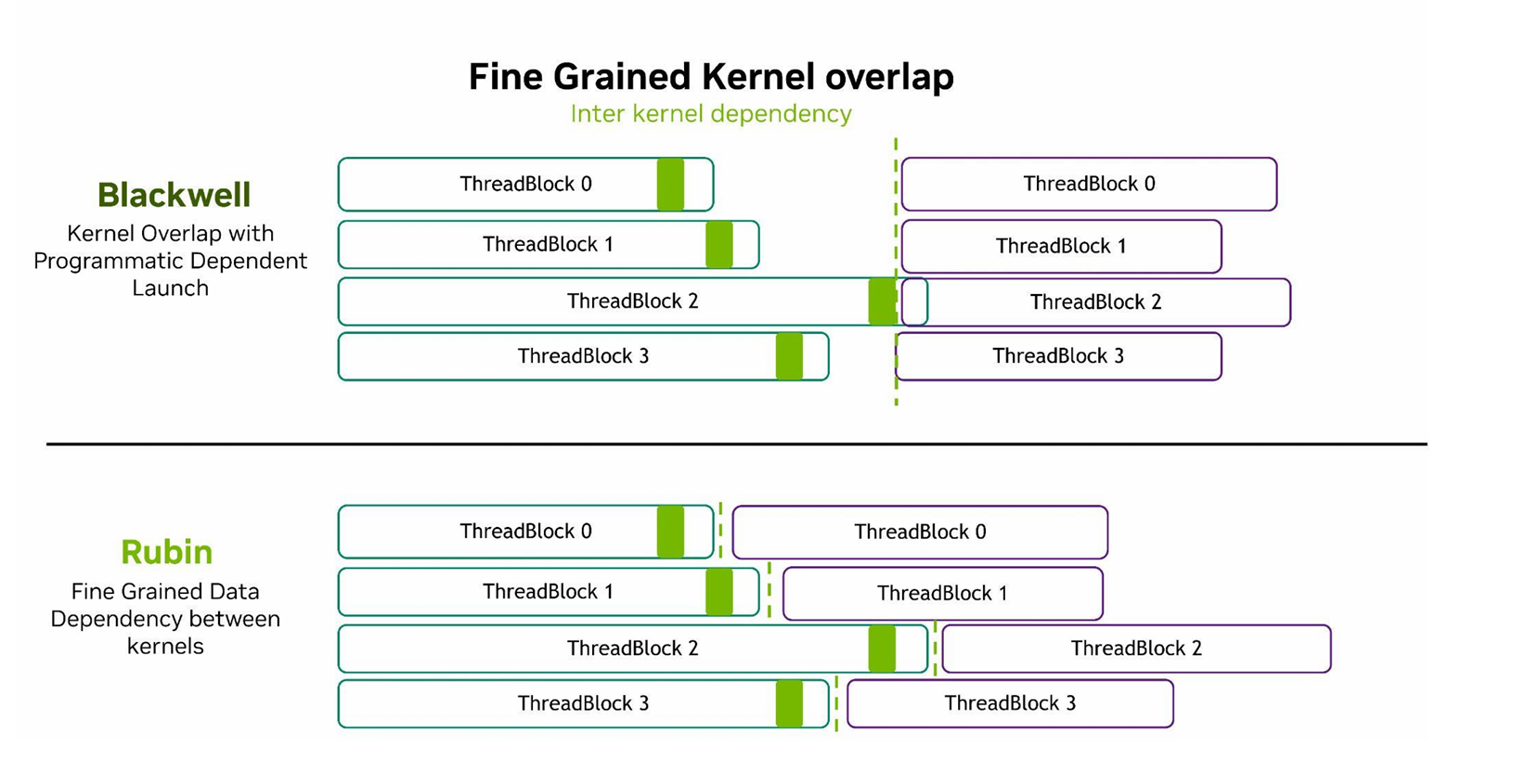
Rubin also increases Tensor Core occupancy by providing finer-grained opportunities for coordination between dependent kernels than on Blackwell. One case that Nvidia cites where these dependencies arise is the generation of activations for an LLM, where one kernel produces and stores data that is then used by a subsequent kernel as a prompt proceeds through a neural network.
(Image credit: Nvidia)
On Blackwell GPUs, a long-running producer kernel on one thread block (perhaps within a CUDA structure like a cluster) might delay the execution of a subsequent consumer kernel on those thread blocks, even as other thread blocks of the producer kernel have finished their work.
Rubin offers finer-grained dependency resolution between kernels, such that a consumer kernel can begin executing on individual thread blocks as soon as the producer kernel’s output from each thread block becomes available, instead of waiting for the entire batch of producer kernel data to become available. This finer-grained management results in better GPU utilization, lower kernel-to-kernel latency, and ultimately increases tokens per second per user.
More efficient inter-GPU communication, lower NVLink overhead
All of the improvements we've discussed so far relate to how work happens on one GPU, but the Vera Rubin NVL72 rack-scale accelerator comprises many GPUs connected over an NVLink fabric within the rack. Model weights, key-value cache data, and inter-GPU synchronization messages all move over this fabric, so keeping overhead and latency low is key to realizing maximum performance.
GPUs running CUDA kernels can directly initiate communication with other GPUs in the rack using Nvidia Collective Communications Library (NCCL) API, lowering overhead. Nvidia notes that because the GPU performs those operations directly as part of the compute kernel, the efficient execution of those communications becomes critical to performance.
(Image credit: Nvidia)
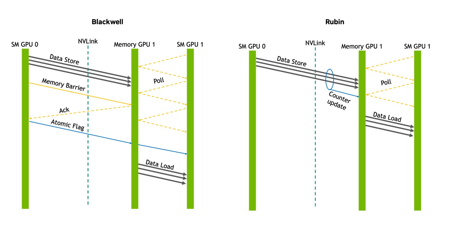
On a Blackwell system, an NVLink transfer between GPUs might require data store operations followed by a memory barrier and an atomic flag. The Rubin architecture introduces a feature called counted writes that reduces the amount of coordination and synchronization traffic necessary to share data between GPUs across the fabric.
On Rubin, the memory barrier and atomic operations are replaced by a single write counter update on the receiving GPU, reducing network traffic and latency and improving compute utilization by reducing the time spent waiting for coordination overhead.
All told, in tandem with the high single-threaded performance of the Vera CPU for agent harnesses, tool calling, code compilation, and more, the improvements in the Rubin GPU for performance on critical inference operations, as well as improved efficiency for data movement on-chip and across the rack, promise to help create a rack-scale and data-center-scale system that will both increase inference performance and lower per-token inference costs in the increasingly agentic future that Nvidia envisions. We’re excited to see more of what this GPU can do as deliveries of Vera Rubin systems are set to begin this fall.
Our local AI testing in 2026 has focused on large language models that can fit entirely into the 128GB of unified memory on Nvidia GB10 and AMD Strix Halo systems. Useful as those smaller open models can be, there is sometimes no replacement for displacement. Today, we’re exploring what’s possible from a local AI cluster with a pair of Nvidia GB10 systems, namely Dell’s Pro Max with GB10 (henceforth Pro Max), which gives us 256GB of RAM for a local AI sandbox.
Quantizing an AI model from higher-precision to lower-precision data types involves tradeoffs for performance and accuracy. And even in quantized form, some advanced open models are still too large to fit within 128GB. But those models can be distributed across multiple local systems using the network as a scale-out backbone, just as they are in the data center.
Why scale out GB10 systems (or Strix Halos, or Macs)? Local token factories with large VRAM pools built up from discrete GPUs can get crazy, fast. Scaling one to even 128GB of VRAM requires a costly host system with enough PCI Express slots and bandwidth to feed those cards, and going beyond 128GB means spending $20K or more in Nvidia GPUs at a minimum, even if you're building up from older 48GB Ada cards.
The preferred recipe for this kind of setup typically includes a Threadripper Pro or Epyc platform, which means a costly CPU, motherboard, and DDR5 kit even before you start adding graphics cards. The power requirements for such a system can quickly get beyond the capabilities of a standard USA 15A circuit (1,800W maximum).
And having four discrete GPUs running their blower fans at high speeds under load, along with whatever other active cooling you might need for what is essentially a GPU server, is not going to make for the most pleasant company if you’re sharing a space with it.
While a GPU server with four RTX Pro 5000 or RTX Pro 6000 cards is useful for getting the absolute best performance for a given application, those potentially high costs, platform challenges, and quality of life concerns have led local AI enthusiasts to explore other ways of achieving large local memory pools with acceptable LLM inference performance, like the GB10 cluster we’re building today.
(Image credit: Tom's Hardware)
Nvidia made the DGX Spark and its Spark-alikes scalable, cluster-able systems right out of the box thanks to their built-in ConnectX 7 200Gbps NICs. These high-end interfaces support Remote Direct Memory Access over Converged Ethernet, or RoCE, so two (or more) GB10 boxes can use them as the backbone for a distributed AI computing cluster.
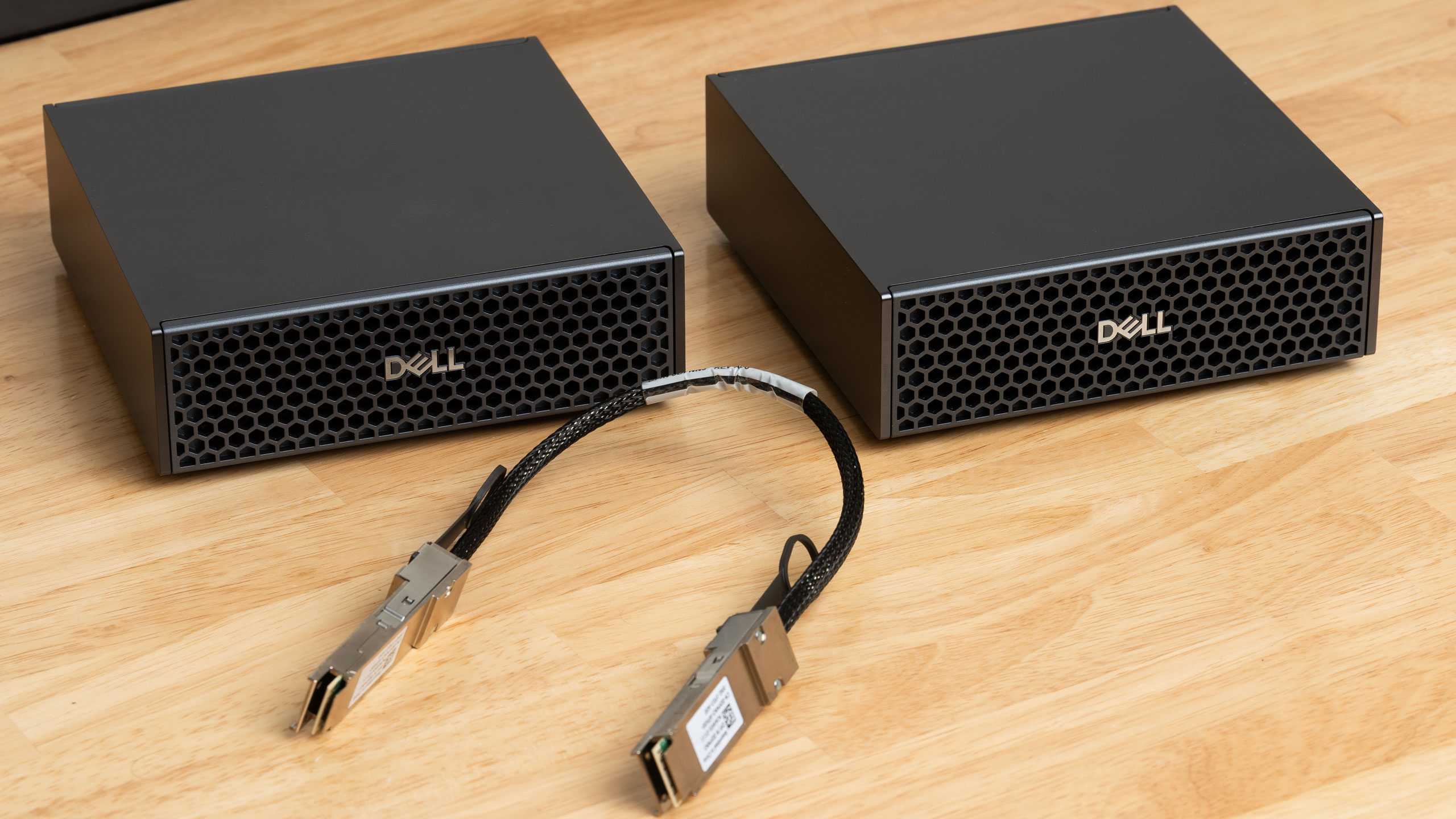
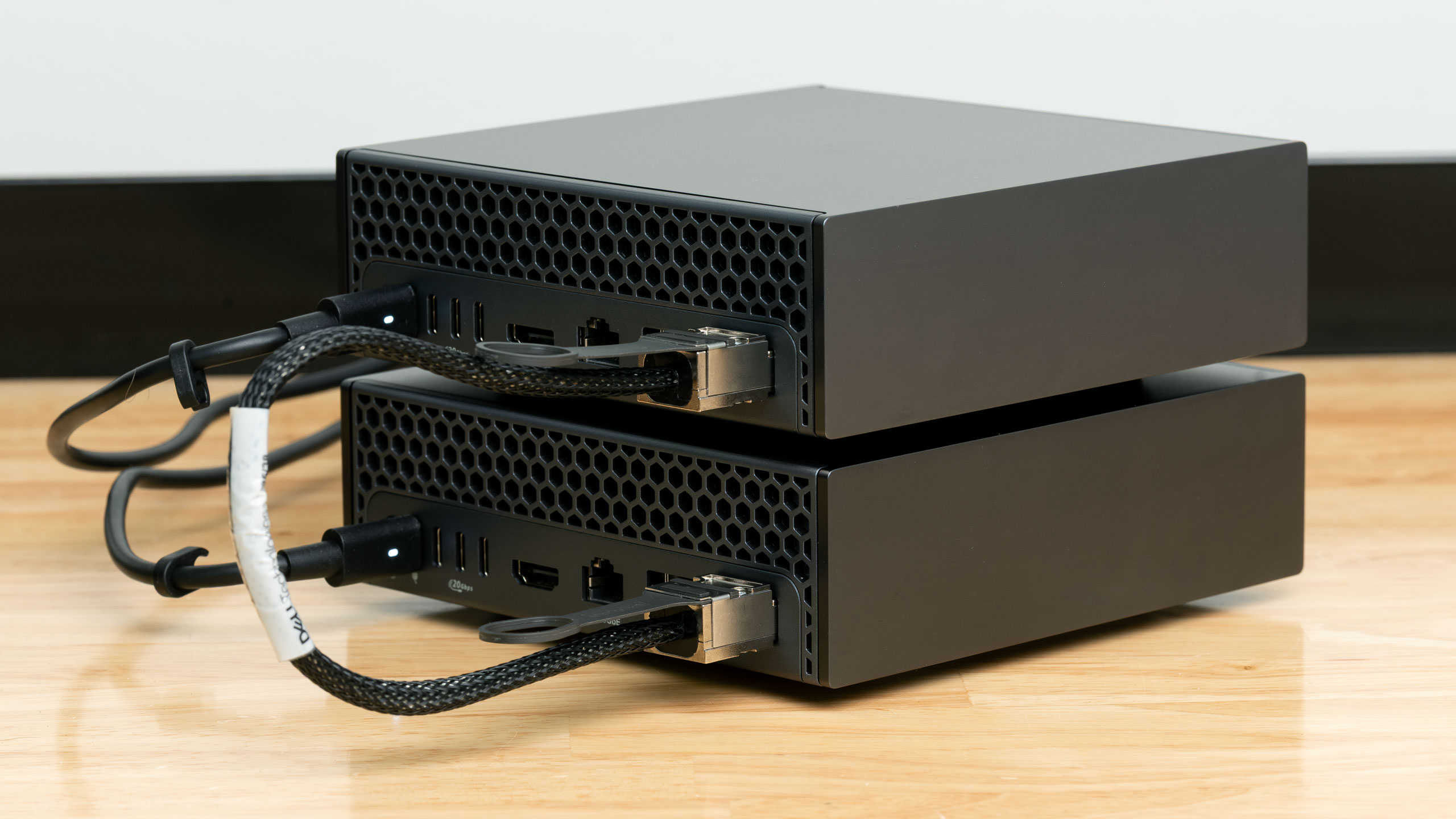
We didn't have multiple Sparks to test RDMA clustering during our initial review, but Dell sent us a pair of Pro Max GB10 systems along with the QSFP cables necessary to join them together.
These systems still aren’t anywhere near cheap, but at $6332 each as of the time of this writing for the tested configuration with 4TB SSDs, you can build a complete, turn-key cluster with 256GB of RAM for less than the cost of the four 48GB or 72GB GPUs you’d need to scale a similar GPU server build.
If you need to save cash and can trade off absolute performance in the bargain, there’s no cheaper way to get into big local models right now, period, but especially not with the level of networking performance that the DGX Spark platform offers.
(Image credit: Tom's Hardware)
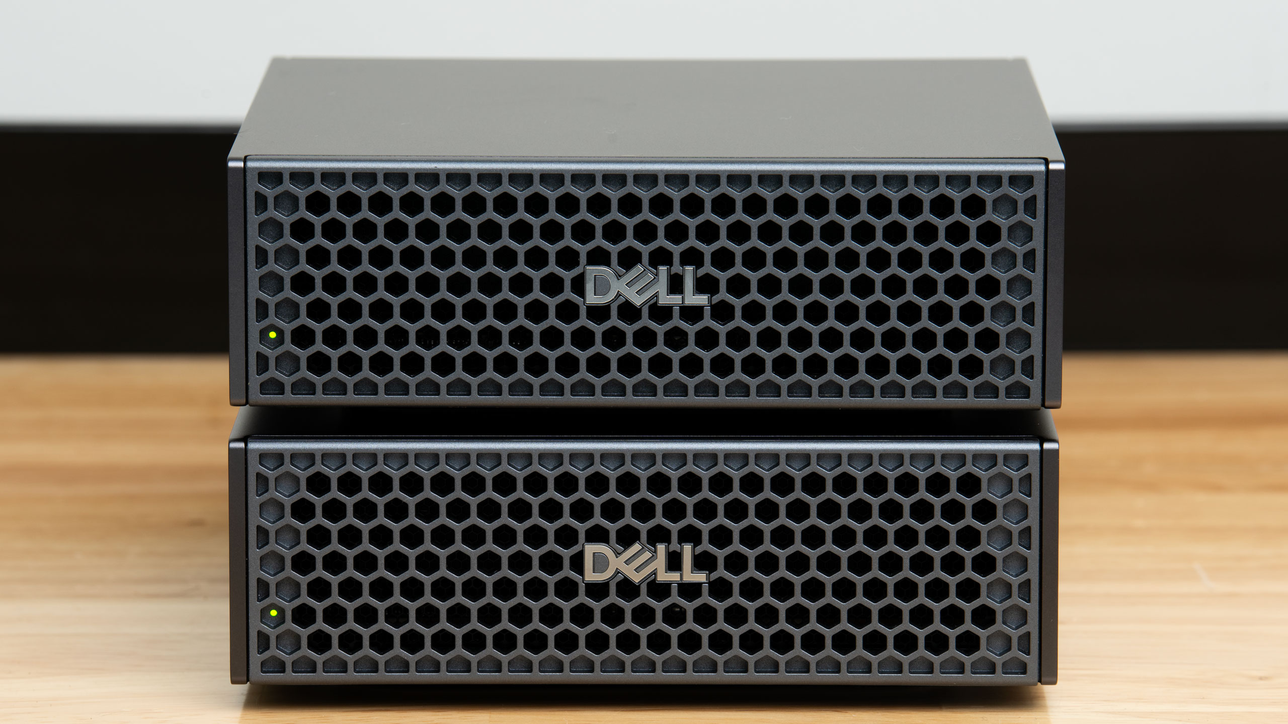
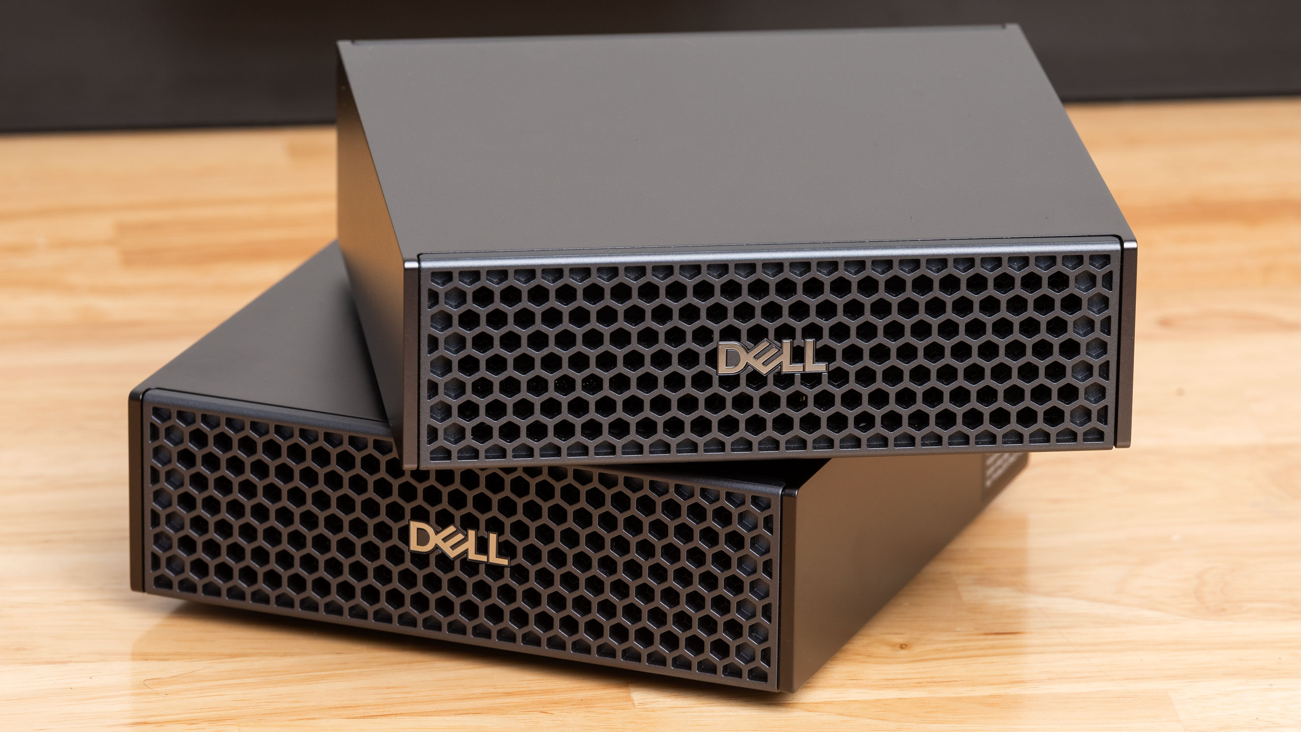
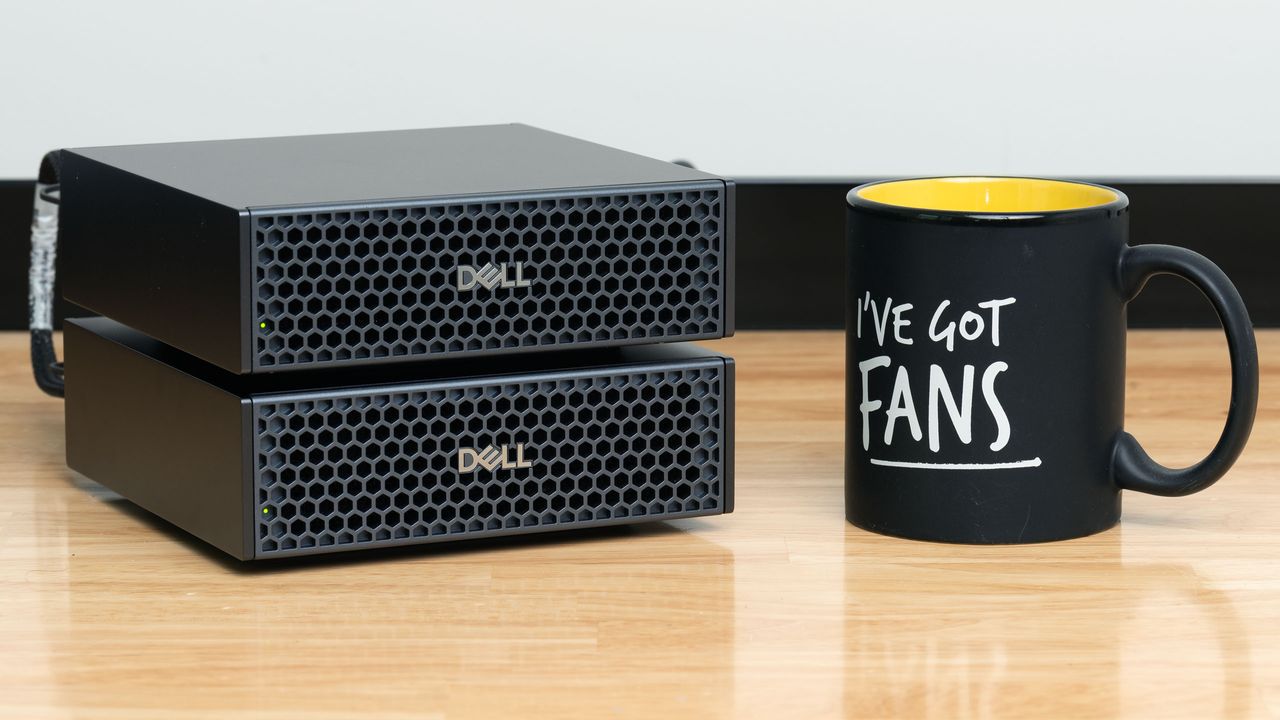
Dell’s Pro Max with GB10 closely follows the Spark template, but it adds an extremely handy power LED to the front panel that the DGX Spark lacks, and the hexagonal grilles on the front and rear panels doesn't catch on clothes or microfiber cloths like the metal foam front and rear panels of the DGX Spark do.
(Image credit: Tom's Hardware)
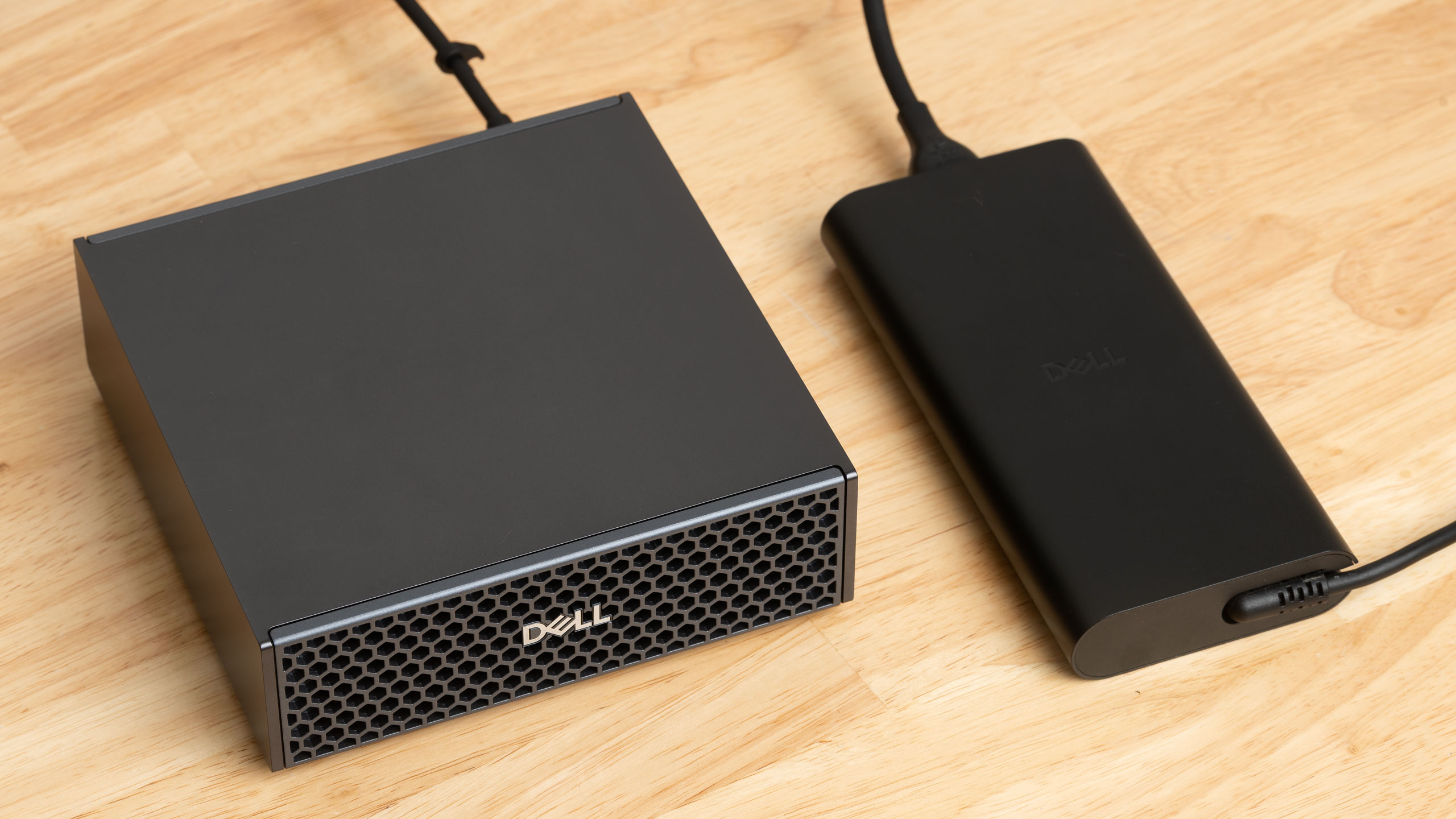
Dell also provides a large 280W USB-C power adapter with each Pro Max GB10 system, or 40W more capacious than the adapter included with the reference DGX Spark. However, there’s nothing to suggest this system has a higher TDP or clocks than the reference Spark design as a result.
Dell Pro Max with GB10
CPU
Nvidia GB10
10x Arm Cortex-X925 10x Arm Cortex-A725
GPU
Nvidia Blackwell GPU, 6144 CUDA cores
Memory
128GB LPDDR5X
Storage
4TB PCIe Gen 4 NVMe SSD
Peripheral and display connectivity
3x USB 3.2 Gen2x2 Type-C ports with DisplayPort Alt Mode support
1x HDMI 2.1b port
Bluetooth 5.4
Networking
Nvidia ConnectX 7 Smart NIC, 200Gbps (QSFP)
10Gb Ethernet (RJ45)
Wi-Fi 7
Operating system
Nvidia DGX OS (Linux)
Power adapter
280W USB Type-C
Dimensions
5.9” x 5.9” x 2” (HWD) (150mm x 150mm x 51mm)
Dell does drop the Pro Max with GB10 back to a PCIe Gen 4 SSD compared to the launch DGX Spark’s Gen 5 drive, but it appears that the ongoing NANDpocalypse has forced Nvidia to source Gen 4 drives for its reference systems to keep costs down, so we’re not holding this decision against Dell here.
Setting up
We’ve already covered the DGX Spark reference design in its own review, so if you’re unfamiliar with the basics of this platform, we’d suggest reading that coverage first. We’ll keep the focus today on the specific challenges and hurdles of clustering two of these systems together.
While the ConnectX 7 NIC on these systems supports both Infiniband and Ethernet protocols in its add-in card form, Nvidia has stated on its official DGX Spark forums that GB10 systems exclusively support Ethernet, and therefore, RoCE for clustering. Don’t buy multiples of these systems hoping to connect them through any Infiniband switches you might have lying around.
The ConnectX 7 NIC on the Spark and Spark-alikes like the Dell Pro Max is also connected to the GB10 SoC in a somewhat weird way due to some possible platform limitations. In short, the largest PCIe bus width one can apparently get off GB10 is a PCIe 5.0 x4 link, so to achieve 200Gbps on any one QSFP port, the two x4 links to the ConnectX 7 have to be teamed behind any one physical port. As a result, each physical port on the NIC is presented to the system as two logical interfaces.
(Image credit: Tom's Hardware)
To achieve the full 200Gbps bandwidth available from the ConnectX 7, you have to configure your networking topology carefully. Nvidia has a Spark playbook on how to do this, and the spark-vllm-docker project also offers its own guide on how to set up these interfaces. I’d recommend following them closely unless you have good reason to roll your own configuration.
After connecting my Dell Pro Max boxes together using the same QSFP cages on their back panels, configuring their network interfaces according to the spark-vllm-docker guide above, configuring passwordless SSH on my second node, and running the recommended NCCL bandwidth test on the link, I found that I was only getting a small fraction of the expected RDMA bandwidth, despite both boxes reporting that they were fully up to date through the DGX Dashboard app.
Community wisdom suggested that a firmware version mismatch was to blame, so I verified that the head Pro Max node in my cluster was fully up to date, both through the DGX Dashboard app and through the command line using the apt package manager.
But even though the DGX Dashboard reported that my second Pro Max system was fully up to date, running the recommended command-line apt checks revealed that there was an update for the fwupd package stuck behind a phasing fence, so I force-installed it.
Once this forced update was complete, it unlocked a new round of firmware updates for the second Pro Max, which I dutifully applied. After rebooting both systems and re-running the recommended NCCL bandwidth tests, I was finally getting something approaching the full 25GB/s one would expect from a proper 200Gbps link.
While none of the issues I had getting my Pro Max GB10 systems clustered were show-stopping, it's also far from a plug-and-play experience. But once both systems were settled in, I didn't see the bandwidth over the ConnectX 7 ports drop back to the degraded performance levels I first observed, even across multiple reboots of the cluster.
Cluster management and performance
If you're thinking about clustering Sparks, you want an inference engine that can handle tensor parallelism, or the distribution of model weights across GPUs during computation. vLLM is an easy choice for doing this on the DGX Spark platform thanks to actively maintained community tools like spark-vllm-docker and sparkrun, but you can also achieve these results with SGLang if that’s your platform of choice.
The spark-vllm-docker project comes with several handy scripts that make starting the cluster and distributing models across it easy, and the sparkrun project provides similar functionality. We focused on spark-vllm-docker for this round of tests, but you have options in this space if you want to explore them.
With our inference engine settled, we went off in search of an advanced model that would utilize a decent chunk of the 256GB of VRAM available from our cluster.
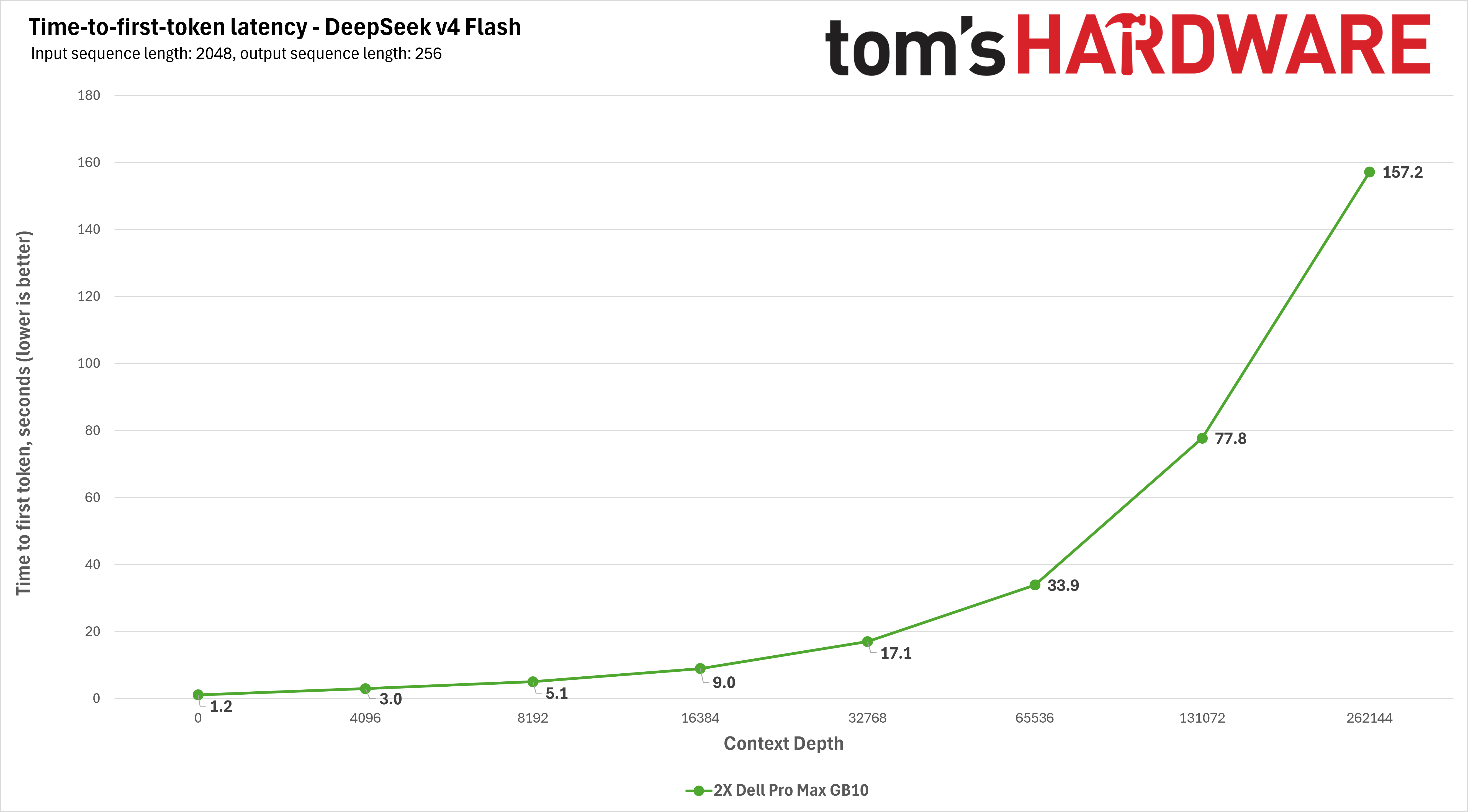
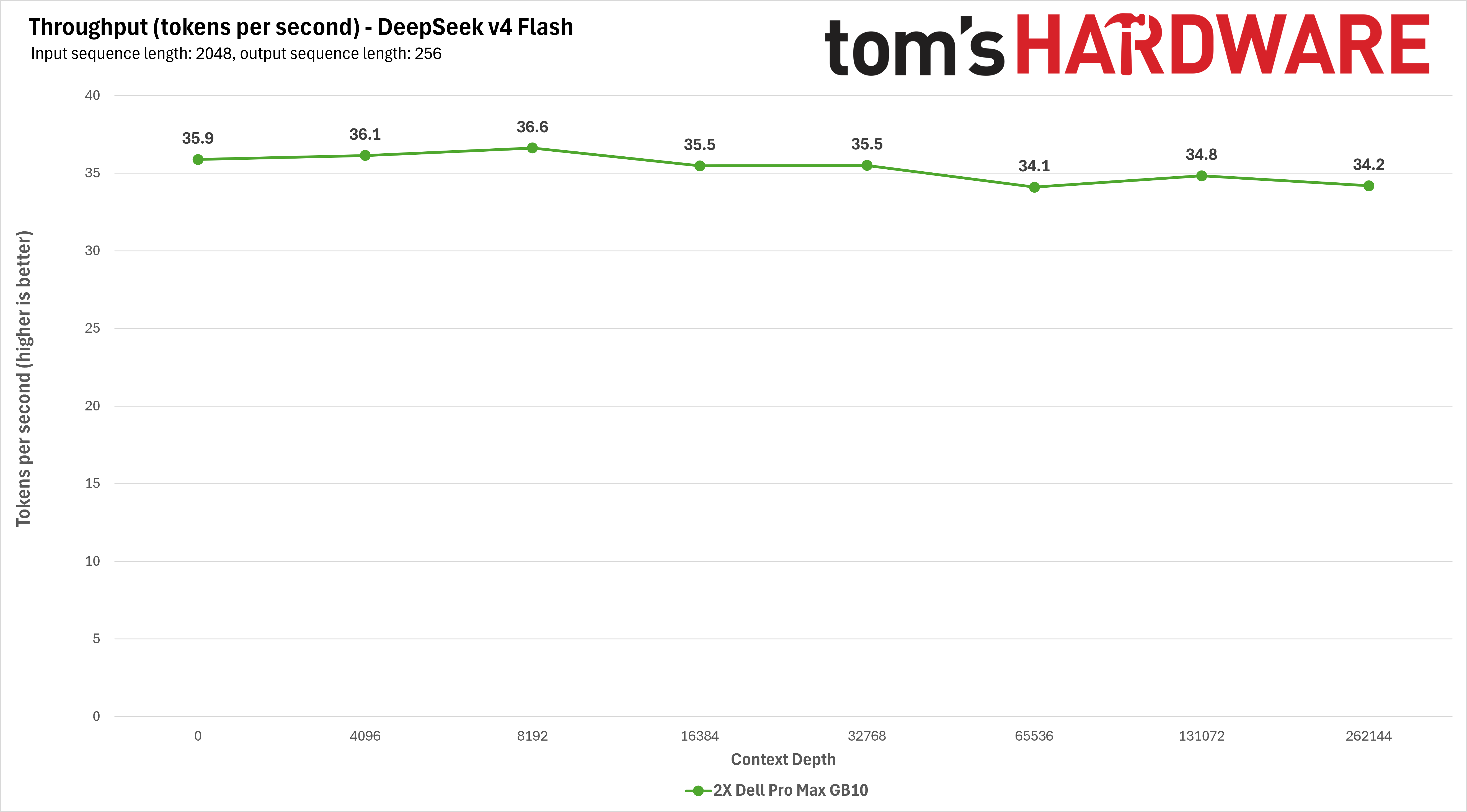
DeepSeek v4 Flash is one such model. It’s a 284-billion-parameter mixture of experts model with 18 billion active parameters per token, and it claims to support a context window of up to 1 million tokens. (vLLM gave us a 400K-token cap on this setup). spark-vllm-docker offers a prebaked vLLM recipe for it, so we downloaded it, deployed it across our cluster, and got to benching.
Tom's HardwareTom's Hardware
The DeepSeek v4 Flash vLLM recipe we used takes advantage of this model’s built-in multi-token prediction capabilities, so decoding throughput remains essentially the same even as time to first token climbs with context lengths up to 200K+ tokens, or about 333 pages of A4 text. That’s impressive and usable performance for a model of this size and capability.
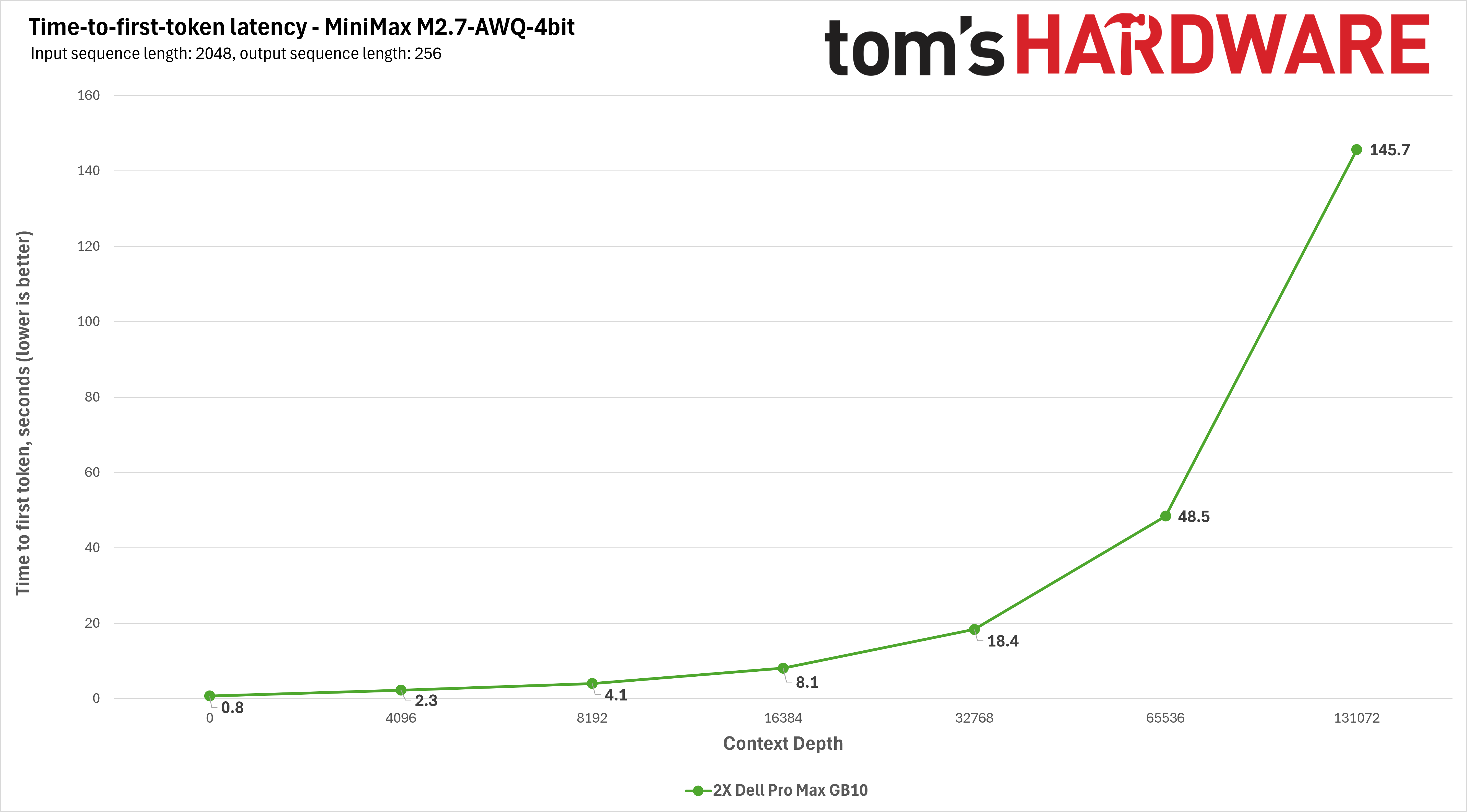
We also loaded up CyanKiwi’s four-bit quantization of MiniMax M2.7. This is another large mixture-of-experts model with 230 billion total parameters and 10 billion active parameters, and it supports a context window out to 200K tokens, which is exactly what vLLM gave us after initialization on our Spark cluster.
Tom's HardwareTom's Hardware
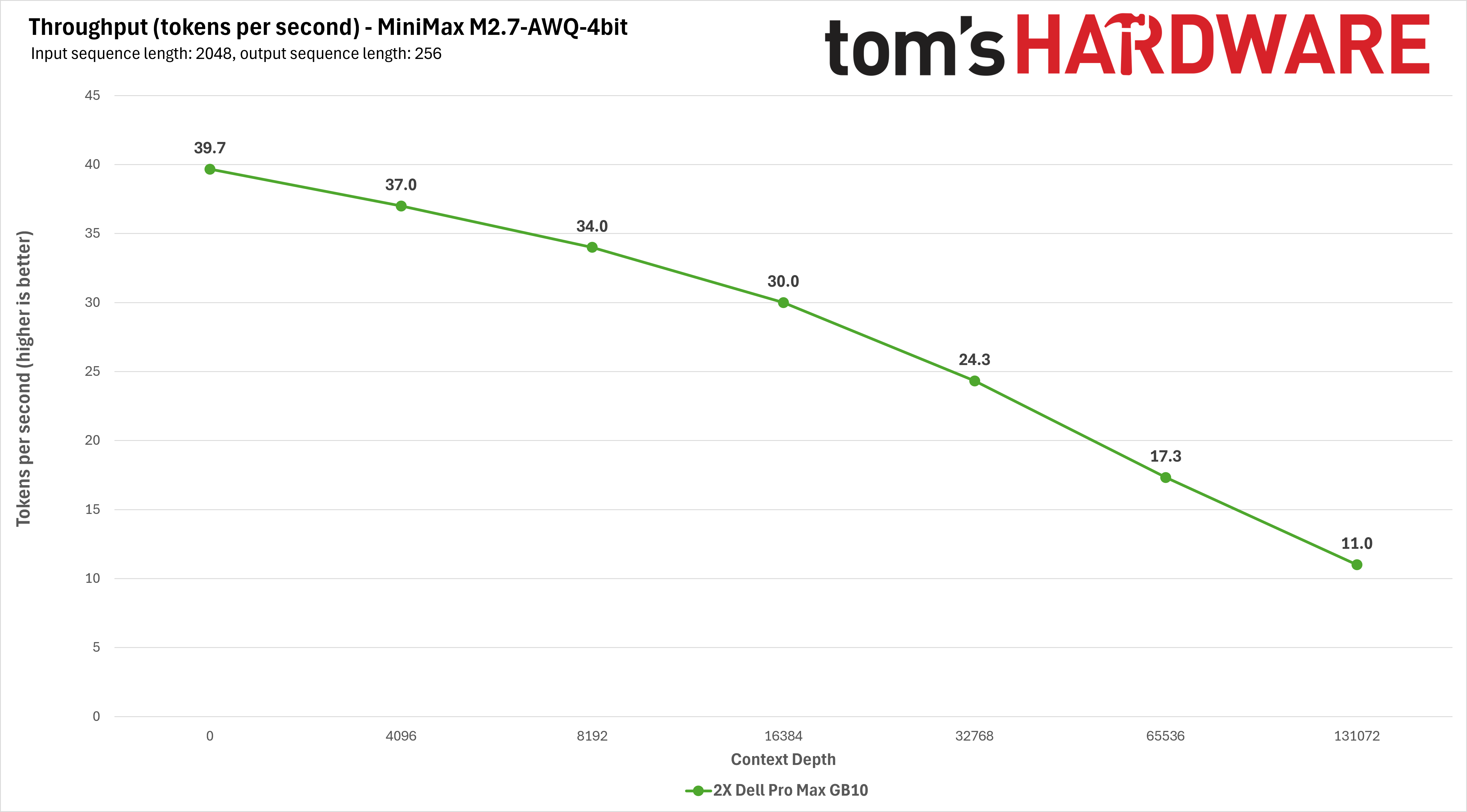
This model doesn’t have the built-in MTP advantage of DeepSeek v4, so even with the four-bit quantization we used for this test, its time-to-first-token and tokens-per-second throughput follow a more familiar curve. Throughput starts in a relatively usable range, but falls off quickly as we approach the limits of the context window.
Our experience running DeepSeek v4 Flash and MiniMax 2.7 shows that even though a Spark cluster isn’t fast, it can still produce enough tokens per second to be a useful sandbox with these demanding models.
Power and thermal notes
As we discussed in our intro, a major advantage of a cluster like this is that it doesn’t require exotic power and cooling to run, and you also don’t have to banish it to a garage or server closet to keep it quiet.
Imeasured peak wall power draw of about 375W to 415W across my cluster during inference performance testing, which is just a bit higher than the TGP of a single RTX 5080 without its host system.
That figure bodes well for adding even more Spark-alikes to a local cluster if you need to, as even four of them running all-out are likely to need less than 1kW from a circuit (before any outboard networking gear is factored in, at least).
Noise levels from my dual Dell Pro Max setup under load were also well controlled, measuring about 40 dBA at 18 inches away. If you need to keep these systems in an inhabited office space or cubicle, they’ll be perfectly tolerable to be around.
If you’re expanding beyond two GB10 systems, I’d guess that any 200G/400G networking gear that you’d need to throw into the mix will likely be far louder than even four of these systems under load, as it’s likely built for a server closet, not a continuously inhabited space.
Bottom line
If you're a local LLM trailblazer and need more VRAM for large, capable models, and don't want to fiddle with or don’t have the cash for a from-scratch GPU server build with more than 128GB of memory, the Dell Pro Max with GB10 cluster we’ve built here exemplifies how clustering Nvidia GB10 systems is a straightforward, space-efficient, low-power, low-noise, and relatively cost-effective way to scale up your local AI sandbox beyond 128GB of VRAM.
(Image credit: Tom's Hardware)
"Relatively" is doing a lot of work here because a pair of Dell Pro Max with GB10 boxes as tested here rings in at $12,664 right now, plus another $50 for the QSFP cable you'll need to hook them together. For organizations or institutions with departmental budgets to spend and existing Dell accounts and support contracts to work within, that dollar figure is likely secondary to the ROI on whatever proposal might drive a purchase order.
But for individuals who just want to build a bigger AI sandbox in their home lab and don't have those relationships to worry about, it's still possible to construct a similar cluster with Asus's Ascent GX10 from stock for under $10K, even at current prices. And as we explained in the intro, going above 128GB of local memory by using multiple discrete GPUs will cost you far more than such a cluster, even before you factor in the cost of a host system.
Not everybody needs to connect multiple Sparks, of course, but if that possibility does intrigue you, the ConnectX 7 NIC in every GB10 box means that there isn't a cheaper way to achieve a 256GB (or larger) distributed memory pool with this class of networking performance behind it.
Some AMD Strix Halo mini-PCs offer PCIe slots for expansion, but they're limited to PCIe 4.0 x4 speeds, so even the funky teamed PCIe 5.0 x4 links to the ConnectX 7 NIC inside GB10 boxes means you're getting far higher potential RDMA bandwidth than you would from adding an aftermarket NIC to a Strix Halo system.
Even though Apple's Mac Studio briefly enjoyed a turn in the spotlight as a cluster-friendly alternative for local AI thanks to the massive memory pools and high bandwidth available from Apple Silicon, along with RDMA over Thunderbolt 5, that star has dimmed, as the company no longer offers memory options larger than 64GB with M4 Max Studios or 96GB with M3 Ultra models. And the lead times on either of those systems are currently over three months out, which is an eternity in the rapidly evolving local AI market.
So Nvidia sort of has this field to itself right now, as GB10 boxes remain readily available from stock with 128GB of RAM at prices that aren't completely bonkers. And if you're a novice to distributed computing concepts, the active community, actively developed tools, and ecosystem software support around GB10 systems are all invaluable for getting your AI cluster running quickly. All that makes Dell’s Pro Max with GB10 (and other Spark-alikes) hard to beat for building a big local AI sandbox to experiment with.
It is now possible to monitor every thermal aspect of Nvidia’s GeForce RTX 50-series (codenamed Blackwell) products, renowned for being some of the best graphics cards you can buy. Thanks to the efforts of Overclock.net (OCN) member asder00, users can now monitor the temperatures for each memory module on Blackwell graphics cards in addition to the recently exposed hotspot sensor.
Nvidia grants direct access to the company's graphics cards and drivers through Nvidia API (NVAPI). Game and software developers employ NVAPI for a range of advanced features. Developers of monitoring tools, specifically, leverage NVAPI to retrieve real-time thermal sensor data so users can keep a close eye on their graphics card's conditions.
While there is a world of information through NVAPI, there are certain sensor readings that Nvidia intentionally kept hidden from developers. Yet, Nvidia's safeguards have not stopped resourceful enthusiasts from discovering creative workarounds to tap into the previously inaccessible sensors. Skilled modders recently managed to gain access to the hotspot sensor, which was only available on internal Nvidia tools like MODS, and now collaboration within the community has enabled individual memory module monitoring.
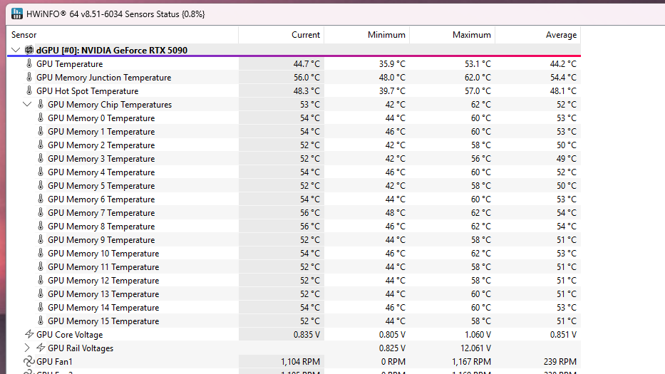
The new plugin, aptly named Hotspot.dll, is specifically for MSI Afterburner. It exists because MSI Afterburner is software from MSI, an Nvidia partner, so it cannot legally poll sensor data not officially made available through NVAPI. Nevertheless, third-party software solutions such as AIDA64 and HWiNFO are not bound by the same partner agreements and will likely add the functionality for individual memory module monitoring the same way they previously adopted support for the hotspot sensor. The latest beta version (v8.51-6304) of HWiNFO already has the function and had no issues reporting the temperature of all 16 of the GDDR7 memory modules inside our GeForce RTX 5090.
(Image credit: Tom's Hardware)
While asder00 developed the plugin, it is important to highlight that it is part of a collective effort. The list of contributors to the breakthrough includes Alexey “Unwinder” Nicolaychuk, the developer behind MSI Afterburner; olealgoritme, known for his work on the open-source Linux GDDR6/GDDR6X temperature reader; Brazilian hardware modder Paulo Gomes; and Martin “Mumak” Malík, the creator of HWiNFO.
The Hotspot.dll plugin reveals the GPU hotspot temperature, die thermal channel readings, average die temperature, GPU memory junction temperature, and per-chip DRAM thermal data. It is compatible with GDDR6, GDDR6X, and GDDR7 memory modules, so it works with the entire Blackwell product stack from the GeForce RTX 5050 to the GeForce RTX 5090. While the original focus of the development was Blackwell, it should work on previous generations of GeForce RTX graphics cards, including the GeForce RTX 40 (codenamed Ada Lovelace) and GeForce RTX 30 (codenamed Ampere) series.
Access to these new sensor readings opens a new level of transparency and control for Nvidia graphics card owners. They will be very beneficial for those who want to fine-tune their graphics card to maximize performance or those who are diagnosing problems.
The upcoming Super refresh of the Nvidia RTX 50-series GPU is reportedly on hold due to the high cost of 3GB GDDR7 memory chips. A VideoCardz source confirmed that one board partner already has RTX 50 Super GPUs on hand, but Nvidia has allegedly told the company that the products are on hold because of the price of 3GB GDDR7 memory chips.
This means that the AI GPU giant has already set an internal release date but is reportedly pushing it back because of memory pricing. If the cost of GDDR7 chips becomes too high, then the RTX 50 Super GPUs would either have a selling price that’s way above Nvidia’s targeted MSRP or, if it forces its partners to stick with or remain close to its set prices, GPU board manufacturers wouldn’t just make any units at all, as they’re going to lose money with every sale.
The RTX 50 Super GPUs are rumored to have 3GB GDDR7 chips, which offers 50% more capacity than the 2GB found in current-gen RTX 50-series graphics cards. This would allow the upcoming GPUs to have more memory without needing to increase or change their memory bus configurations.
According to the publication, the cards expected to be released soon include the RTX 5080 Super, RTX 5070 Ti Super, RTX 5070 Super, and RTX 5050 9GB. The first two will each receive 24GB of GDDR7 VRAM with a 256-bit bus width, while the RTX 5070 Super will have 18GB of VRAM with a 192-bit bus width. Unfortunately, these chips cost twice or thrice as much as their 2GB variants, which will likely push the retail price of these cards beyond Nvidia’s envisioned MSRP.
Nvidia used to supply VRAM chips alongside GPU dies to its board partners, but it changed this policy in late 2025 as the memory chip crisis unfolded. Because of this, the companies that complete the final assembly of the graphics cards are forced to source their own memory chips in an increasingly competitive market. SK hynix, one of the big three memory chip manufacturers, even says that 2027 is set to be the “worst year” for the memory shortage and said that the crunch will last until 2030.
Even Nvidia, one of the biggest winners in the AI race, has been affected by the RAMpocalypse, with the company not announcing a new GPU at CES 2026. This is the first time this has happened in five years, with Jensen Huang releasing the 30-series, 40-series, and their respective mid-generation refreshes despite supply chain limitations and several other issues that arose during that period. Its latest AI systems are now more expensive than ever, with memory accounting for 25% of the BOM, as costs have soared by nearly 500%.
It’s still unclear what Nvidia and its board partners plan to do about the memory situation, especially as things don't seem to be improving. While it could delay the launch of the RTX 50 Super, it can only do so for so long, especially if it’s true that its dies are already in the hands of its board partners.
Nvidia today announced that it's working with Japan's Noetra Corp. to build a 140-megawatt AI factory packing 27,500 Rubin GPUs and 13,750 Vera CPUs, the compute foundation for FRONTia, the Japanese government's state-funded physical AI program. The facility will be built from Vera Rubin NVL72 racks on Nvidia's DSX reference platform, connected with Spectrum-X Ethernet, and will train open multimodal foundation models for robotics, digital twins, and industrial automation, with pretrained weights shared broadly with domestic developers.
"Japan invented modern manufacturing. Now, it is building the AI factories that will power the next industrial revolution," said Jensen Huang, founder and CEO of Nvidia, in the announcement.
The chip counts divide exactly into 382 Vera Rubin NVL72 racks, each housing 72 Rubin GPUs and 36 Vera CPUs. Neither company disclosed the project's cost, but VR200 NVL72 systems are currently quoted at $5 million to $7 million apiece, which puts the rack hardware alone somewhere between $1.9 billion and $2.7 billion. Morgan Stanley estimates Nvidia will charge $55,000 per Rubin GPU in volume, pricing the GPU silicon at roughly $1.5 billion before memory, networking, and cooling.
No deployment timeline was given in the announcement, but Rubin racks are only expected to reach volume production in the second half of this year, and Nvidia said the facility will support trillion-parameter model training "as the AI factory expands," suggesting a phased ramp.
Noetra is a new consortium founded by SoftBank Corp., Sony, NEC, and Honda, with investment from 44 companies and organizations, NEC said in a press release also published today. Noetra and the national research institute AIST won a NEDO public tender on June 30 to run the FRONTia project from fiscal 2026 through fiscal 2030, with ¥387.3 billion (roughly $2.4 billion) in first-year funding and up to ¥1 trillion (roughly $6.1 billion) over five years, Asia Times reported. Funding beyond the first two years is subject to annual stage-gate reviews, so the full amount isn't guaranteed.
Noetra's roadmap targets a reasoning foundation model in fiscal 2026, an omni-modal model that processes text, images, video, and audio by fiscal 2028, and "real-world native AI" capable of spatial awareness by fiscal 2030, per NEC.
The AI factory follows SoftBank's Blackwell-based DGX supercomputer, announced in 2024, and FugakuNEXT, the $740 million RIKEN, Fujitsu, and Nvidia zetta-scale system due around 2030, but it's the first that's state-tendered national infrastructure rather than a corporate or scientific machine. Japan's AI Robotics Strategy, released in March, targets more than 30% of the global AI robotics market by 2040, an opportunity the government estimates at $133 billion.
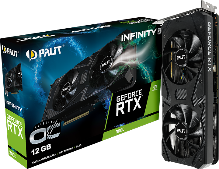
Nvidia has just relaunched its five-year-old graphics card, the GeForce RTX 3060, in order to combat the component scarcity driven by AI. This resurrection has seen a staggered release, with companies like Gigabyte and Manli silently listing their renewed variants in different parts of the world. Today, Palit joined the list with an official announcement for its RTX 3060 Infinity 2 OC, the first official indication of Ampere's return.
If we take a look at the specs, the card is identical to the original RTX 3060 we saw in 2021 — it has 3,584 CUDA cores paired with 12GB of GDDR6 VRAM saturated across a 192-bit-wide bus. Since this is an overclocked variant, it can boost up to 1,792 MHz, which is less than 1% higher than the base 1,777 MHz boost that Nvidia already mandates. Palit will also release a non-OC variant of the Infinity 2 RTX 3060.
The card features a relatively simple design characterized by the typical black aesthetic we see on budget GPUs. There's no zero-RPM tech here, but Palit claims 0dB noise levels and says there's a "protective backplate" on the card that prevents PCB flex. When you're buying a GPU like this, its looks are probably the least of your concern; the main selling point is, of course, that 12GB memory pool.
PalitPalitPalit
Late last year, the PC hardware industry entered one of its most turbulent eras, characterized by production inadequacies created by the AI boom. Artificial intelligence demands a lot of memory and storage, and thus, commodity silicon has skyrocketed in price overnight with no signs of slowing down. After evading the crisis initially, GPUs eventually got wrapped up in the price hikes as well.
Nvidia's latest Blackwell family uses cutting-edge GDDR7 memory, which is even more expensive, and since vendors are busy producing HBM for fatter margins instead, the "solution" to this dilemma had to be creative. The idea for reviving older generation cards was actually floated by our very own Paul Alcornat a Q&A at CES 2026, where Nvidia CEO Jensen Huang replied, saying he'd "go back and take a look at this."
Palit hasn't provided a price for the Infinity 2 OC yet, and we didn't see it listed on retailers yet, but we can infer it'll cost around $329 given similar variants have also been popping up for that price. To be clear, the RTX 3060 is a great value GPU that we praised even back when it launched. But in the face of the RTX 50-series, it's not exactly something you should consider first, especially when buying new.
You can get an RTX 5060 Ti for just $369 right now on Newegg, which is a significantly faster card with support for DLSS 4.5 and multi-frame gen, not to mention the better efficiency. It only has 8GB of VRAM, unfortunately, which hurts performance at high resolutions and if you like to play with ray tracing enabled. Still, unless you're going up to 4K, the 5060 Ti (and the regular 5060) will perform much better than a 3060 no matter what, as you can see in our GPU benchmark hierarchy.
Ultimately, rebooting the RTX 3060 makes sense from a manufacturer's point of view given the better yields of Samsung's older 8nm process compared to TSMC's more expensive N5 node used by Ada and Blackwell. But as a consumer, you should definitely stick with the RTX 50-series or try to find a used RTX 40-series GPU instead.
If you're looking for a relatively affordable graphics card upgrade, the landscape has been barren of late, even during the peak of Prime Day. But Amazon is back with a deal on Asus' Prime RTX 5060 that beats even the best Prime Day lows we saw — at least if you're one of the lucky Prime subscribers it deems worthy.
If you do qualify, you can get this card for just $301.62, or just $2 above MSRP, which is as low a price as you'll find anywhere for an RTX 5060 right now.
To get this deal, you need to be a Prime member, but you also need to meet some other secret criteria. Most of the Tom's Hardware staff and several friends were eligible for the discount, but at least one of my friends didn't see it despite being a Prime member, so it's not a surefire deal. That said, if you are lucky enough to get this offer and need an affordable GPU upgrade, it's worthy of your consideration.
Nvidia's GeForce RTX 5060 is our pick for the best 1080p gaming graphics card, and you can score this Asus Prime card and its spiffy triple-fan cooler for less right now.View Deal
Despite having 8GB of VRAM, the RTX 5060 offers some of the strongest bang for the buck of any graphics card of its class, thanks to the strong baseline performance of its Blackwell architecture and support for the latest DLSS 4.5 upscaling model (as well as MFG, if your game's VRAM usage is low enough to allow for it).
The recently re-introduced RTX 3060 12GB is selling for anywhere from $329 to $359, but despite its extra 4GB of VRAM, we wouldn't give that card a second glance in 2026. By the time the extra VRAM makes a difference in performance, you're already running into the limitations of this five-year-old graphics card's shader horsepower. And even in raster games, the 3060 greatly trails the 5060 in our 2026 test suite. The smart money is definitely on the more modern Blackwell card.
The RTX 5060's most direct competition is the $299 Radeon RX 9060 XT 8GB, but you won't find any of those cards for anywhere close to the price of the median RTX 5060 right now, to say nothing of this Asus Prime card.
Versus other RTX 5060s, the Prime RTX 5060 8GB stands out thanks to its triple-fan cooler, sleek and stealthy shroud, and a full-length backplate with a large flow-through cutout for waste heat. Asus also equips this card with a dual-BIOS switch that lets you choose between the highest performance and low noise levels.
All that adds up to a great deal, so if you need an entry-level gaming upgrade in 2026 and qualify for this coupon from Amazon, you should jump on it while you can.
MSI Afterburner’s solo developer is working on a new update that provides a heatmap of the most-used voltage/frequency points a GPU is operating at within Afterburner’s voltage/frequency curve chart. The update is designed to help enthusiasts and overclockers better understand the boosting behavior of their GPU and adjust their GPU’s overclock accordingly. Unwinder, Afterburner’s developer, reported on the Guru3D forums that this update will be released with 4.6.7 beta4 for users to test. An official (non-beta) release with the heatmap has not been announced yet.
The new heatmap generates yellow dots within Afterburner’s existing V/F curve editor, making it easy to compare the GPU’s existing V/F curve against where the GPU is boosting in real workloads. For instance, Unwinder shared a screenshot of the heatmap being used with an RTX 5090, showing the GPU operating primarily at 800mv at 1200MHz, and 1000- 1055 mV at around 2.6 to 2.8GHz. The former relates to the GPU’s behavior at idle/low-load workloads and the latter at maximum load.
the next beta of msi afterburner developed by unwinder adds V/F hit map.v4.6.7 beta4 (not yet released)https://t.co/sJxErlqMLVthe current latest beta is v4.6.7 beta3 build17352 (jun 19)https://t.co/o4jRfXFMJP https://t.co/cEMaQHaDTe pic.twitter.com/7vKK0rgyhhJuly 12, 2026
Unwinder revealed that one interesting perk of the new heatmap system is its ability to identify the differences in boosting behavior between Nvidia’s RTX 40-series and older GPUs, and RTX 50-series GPUs. Improvements in Blackwell’s DVFS, or Dynamic Voltage Frequency Scaling, make the GPU behave very differently compared to RTX 40-series GPUs or older. Unwinder shared an additional screenshot of an RTX 4090 running the heatmap, showing yellow dots only around the lower and upper ranges of the V/F curve. By contrast, the heatmap of the RTX 5090 shows yellow dots across the entire V/F curve, revealing that the RTX 5090 is spending more time in the middle range of the curve than its predecessor.
MSI Afterburner’s new heatmap aims to help overclockers more accurately adjust their overclocks according to what voltage/frequency points the GPU is prioritizing in real workloads. For the uninitiated, V/F curve overclocking manipulates the GPU’s boosting algorithm by changing the shape of its V/F curve. If you're able to sustain the same clock speed at a lower voltage, that should mean a higher voltage can push a higher clock speed, which is the idea behind undervolting with a V/F curve before overclocking with an offset.
AMD is reportedly testing FSR Multi Frame Generation for existing Radeon GPUs, with ratios of up to 8x. According to a screenshot shared on the Chiphell forums, AMD's latest Adrenalin Edition 26.6.2 driver includes support for Multi Frame Generation, as hidden experimental settings were discovered in RadeonTuner, a third-party open-source alternative to AMD Adrenalin Software. In addition to a new Multi Frame Generation Ratio setting, RadeonTuner also includes override options for FSR Ray Regeneration Denoiser and FSR Neural Radiance Caching.
This suggests that AMD is potentially testing FSR Multi Frame Generation, with options ranging from 1x to 8x. In theory, that could boost a base frame rate of 60 FPS to as high as 480 FPS, which is around 2x higher than what Nvidia currently offers on its RTX 50 series GPUs. That said, these settings are non-functional, and there is no confirmation whether AMD has plans to roll out an 8x Multi Frame Generation mode.
(Image credit: Chiphell Forums)
The discovery has also prompted a response from the developer of RadeonTuner on GitHub, where they explained that AMD occasionally adds the names of upcoming settings to its drivers months before the actual functionality is implemented. The developer also clarified that the newly listed Multi Frame Generation ratios of up to 8x are placeholders that have been added for testing purposes, meaning that it may or may not align with the final implementation that AMD ends up supporting eventually.
Interestingly, during Microsoft's recent unveiling of its upcoming Xbox platform codenamed Project Helix, the company confirmed that the console will feature FSR Diamond (previously called FSR Next). This was touted as an AI-powered rendering suite that would include machine learning-based upscaling, ray regeneration, and Multi Frame Generation. AMD's graphics chief, Jack Huynh, later described FSR Diamond as the result of a multi-year engineering collaboration with Microsoft.
While there is no indication that the hidden driver settings are directly tied to FSR Diamond, the presence of experimental options for Multi Frame Generation, Ray Regeneration, and Neural Radiance Caching suggests AMD is laying the groundwork for its next-generation FSR technologies across the Radeon ecosystem.
When the RTX 50 series launched, reviewers quickly discovered that the hotspot temperature was being misreported in standard diagnostics tools such as HWiNFO or MSI Afterburner. Eventually, people realized that Nvidia had outright removed the option to monitor hotspot temps, but it seems like the hardware was never removed from the GPU. New testing by Brazilian repair specialist Paulo Gomes has revealed that the sensor is still present and readable with special tools.
In the video, the host shows a Gigabyte variant of the RTX 5070 Ti that was sent to him due to overheating issues. Within Windows, the monitoring tools showed no abnormal signs, as the "average" temperature was reported at 67 to 68 degrees Celsius. However, when diagnosed with a specialized tool called "MODS," the hotspot temperature reached 107 degrees Celsius almost immediately under load.
MODS stands for Modular Diagnostics Software, and it's an internal Nvidia tool used to test GPUs before they hit the shelves or during the RMA process. It's not available to the public and doesn't work on Windows because the OS keeps intercepting calls from the hardware monitoring APIs. You need a Linux distribution that boots directly into a command line, from where MODS (and MATS, for memory testing) can run as intended.
Some repair shops have been known to get access to MODS, such as in this case, which unlocks the hidden hotspot temperature sensor on Blackwell gaming GPUs. Keep in mind that Nvidia ships much more comprehensive diagnostic utilities for its server-grade and workstation GPUs that can actively monitor all aspects of the card. It's unknown why the company decided to keep some sensors locked out of gamers' reach.
Perhaps we can infer the rationale from last year, when Igor's Lab tested several RTX 50-series GPUs and found a "hotspot issue" affecting all of them. The reason was poor PCB manufacturing — not using heavy-duty materials to build the PCB layers, causing certain parts of the substrate to heat up even when the core was relatively cool. This was exacerbated by Nvidia's own guidelines, which told AIBs to compensate for ideal conditions instead of worst-case scenarios.
Anyhow, as Paulo Gomes and his team discovered, the RTX 5070 Ti's hotspot was hitting 107 degrees Celsius, and the card throttled and dropped its clock speeds right away. Nvidia mandates 107 degrees Celsius as the upper limit for RTX 50-series, so it was clear that the card was slowing down to prevent damage. To inspect what was actually wrong, they opened up the card and found poor thermal contact between the cooler and the componentry.
The TIM (thermal interface material) application was inadequate; the paste had accumulated around the perimeter of the core while the center was mostly dry. The repair personnel removed the old material and replaced it with SnowDog Husky paste, which was enough to drop the hotspot temperatures to 100 degrees Celsius. Now, it was within the safe operating range and no longer thermal throttling under load.
What would've been a simple fix on the consumer's end was turned into a repair job solely because Nvidia hid the GPU's hotspot temperature, literally misreporting the card's internal condition. Had this RTX 5070 Ti just run at 107 degrees Celsius continuously, the silicon would wear down incredibly fast, and the customer would never even know why. Not to mention some manufacturers' insistence on voiding warranty upon breaking the GPU's "seal," which is an illegal and unenforceable practice in the United States.
AMD’s formerly China-exclusive Radeon RX 9070 GRE, which rivals the best graphics cards, went global last month at a suggested MSRP of $549. The GPU has now seen its first price drop since its launch, with the Gigabyte Gaming Radeon RX 9070 GRE available for $499 at Newegg. While the listing shows $549, customers can use a $50 promo code by submitting their email address to reveal it.
The Radeon RX 9070 GRE is built on AMD’s RDNA 4 graphics architecture, and uses the same Navi 48 GPU as the Radeon RX 9070 and RX 9070 XT. However, it uses a cut-down version of that chip with 48 compute units. It also comes with 12GB of GDDR6 running at 18 Gbps on a 192-bit bus, offering 432 GB/s of raw memory bandwidth. Despite the scaled-down specifications, the RX 9070 GRE retains a TDP of 220W, similar to the standard Radeon RX 9070. Essentially, the card sits between the RX 9060 XT 16GB and the RX 9070, and AMD claims it delivers 21% higher average performance than the RTX 5060 Ti 16GB in 1440p gaming.
FutureFutureFuture
In our testing of the XFX Swift Radeon RX 9070 GRE, we found that the card averages 120 FPS at 1080p and 86.6 FPS at 1440p across our 11-game raster-only test suite. That makes it a solid choice for high-refresh-rate gaming at two of the most popular monitor resolutions, and it offers a comfortable position over the RX 9060 XT 16GB and RTX 5060 Ti 16GB.
Unfortunately, the RX 9070 GRE is not entirely impressive at 4K resolution as it struggles to maintain an average of 60 FPS. That said, enabling FSR 4 upscaling and frame generation in supported titles can significantly improve performance. Ray tracing performance remains a weaker area for the RX 9070 GRE. Gamers who prefer enabling RT effects will likely need to enable FSR 4 to offset the performance hit, particularly at higher resolutions.
At its discounted price, the RX 9070 GRE competes directly with Nvidia's RTX 5060 Ti 16GB, which currently sells for well over $500. If you are a gamer who prioritizes raw rasterized performance, the RX 9070 GRE is worth considering, especially if you're upgrading from an older GPU such as the RX 6700 XT or RTX 3070.
 登录
登录